Chip binning is the factory sorting of finished silicon into performance grades, and overclocking headroom is the gap between the clock a chip is guaranteed to hold and the clock it will actually reach under load. Binning is a deliberate decision made at test; headroom is what is left over after that decision, and it varies from part to part.
The confusion between the two causes most of the wrong expectations in this area. People hear “high bin” and assume it means a chip that overclocks well, when the two are measured by different tests and often rank parts in the opposite order. This guide separates them, walks through what happens between wafer and product label, and gives a method for judging extra performance on a chip you already own.
Here is the short version: binning is a factory decision made with calibrated equipment, and headroom is what you find when you test the part in front of you. Those are different things, measured by different tests, and keeping them apart explains most of the disappointing results people report.
Table of Contents
- Chip Binning and Overclocking Headroom Explained
- What Is Chip Binning and How Does It Work?
- What Is Overclocking Headroom?
- Why Do Chips From the Same Product Line Behave Differently?
- Threshold voltage and leakage current
- Random dopant fluctuation and line edge roughness
- How Manufacturers Test Chips Before Sale
- How to Estimate Overclocking Headroom Safely
- Headroom for CPUs, GPUs, Memory, and Other ICs
- Chip Binning and Overclocking Headroom Explained in Practice
- Frequently Asked Questions
- Does chip binning mean every chip has a different maximum speed?
- Is overclocking headroom guaranteed for chips with the same model number?
- Why can a lower-binned CPU overclock better than a higher-binned one?
- How much voltage increase is normally needed for extra performance?
- Can overclocking reduce a processor’s expected lifespan?
- Does cooler memory or a stronger motherboard create more chip headroom?
- Conclusion: Start With Ratings, Then Test Carefully
Chip Binning and Overclocking Headroom Explained
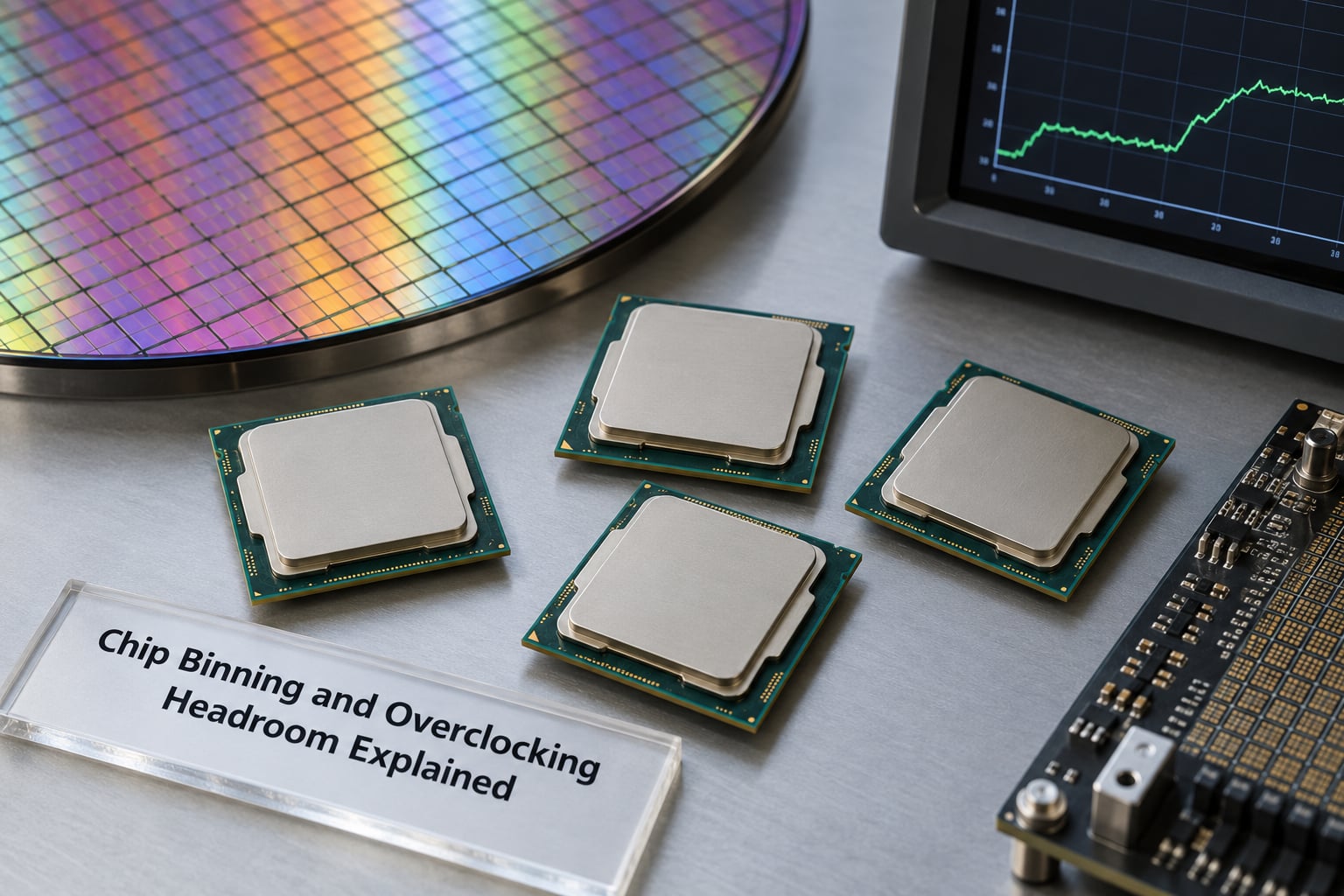
Chip binning is the post-fabrication sorting of finished dies into grades based on measured test results, so each die is sold under a product name matching what it can actually achieve. Overclocking headroom is the remaining distance between that guaranteed specification and the chip’s practical thermal, voltage and stability limits.
Three different parties get involved, and mixing them up causes most of the argument online. Manufacturer binning happens at wafer sort and final test, measured on calibrated equipment, and the result is written into the part number, the fuse table and the datasheet. Retailer selection happens weeks or months later, when a shop grades already-binned stock by cosmetic condition, sometimes sorting by the date code or lot code on the label. Enthusiast selection is what a buyer does after unpacking, running a few hours of tests and deciding whether to push further.
A guaranteed specification is a floor with a ceiling attached. A processor sold at a stated boost clock is warranted to reach that clock, at a stated voltage, at a stated junction temperature, across a stated temperature range, on a qualified board. Every one of those qualifiers is load-bearing, and removing any of them is how an “unstable overclock” turns out to have been a stable spec all along.
Additional performance is what remains after those qualifiers are satisfied. That remainder exists because a design team has to ship a part that works for every unit of every lot, in every chassis, at every ambient temperature, for years. The margin between the worst unit and the guaranteed number is headroom, and the design team’s decision about how much of that margin to hand to you is a commercial choice as much as an electrical one.
What Is Chip Binning and How Does It Work?
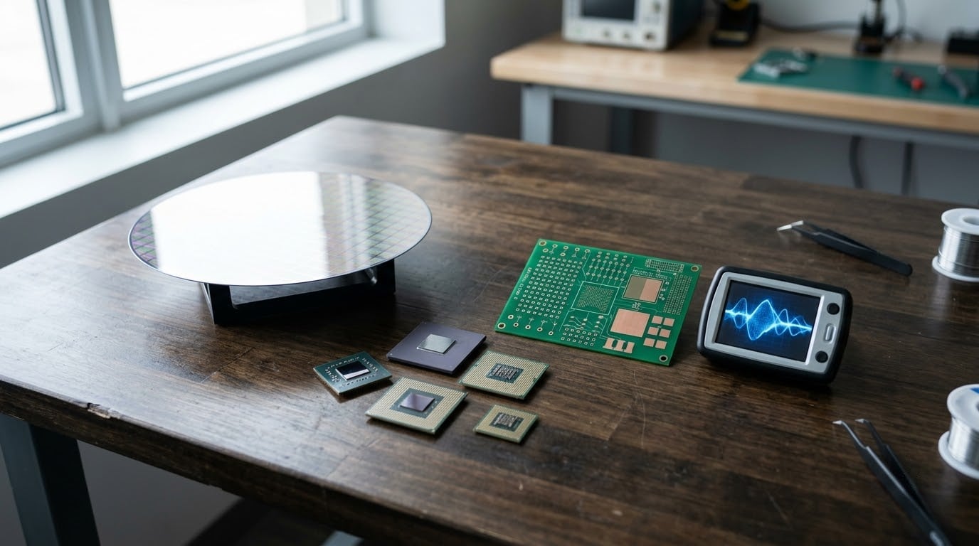
Binning works because no two dies from the same wafer are electrically identical. A foundry prints hundreds or thousands of copies of a design onto each wafer, then probes them individually. Every die that fails a limit is thrown away or salvaged for a lower product, and the ones that pass are sorted into groups by how much they passed by.
Sorting begins at wafer sort, where a probe card lands thousands of contacts on the die’s pads and a tester measures it while it is still part of the wafer. This is the cheapest point at which to reject a part, because a defective die that is caught here costs a fraction of what a packaged, tested and binned one costs.
Measurements made at that stage feed the bin decision. Speed grade binning uses fmax, the maximum frequency a die sustains at a given voltage and temperature across a defined pattern set. Power binning uses current draw and leakage at load, which matters enormously in a phone or a server socket where the power envelope is fixed. Core-count binning takes a design with more functional units than the product needs and disables the surplus, usually through on-chip fuses rather than by any change to the silicon. Feature binning removes a block entirely, such as a cache slice, an error-correction unit or a reliability, availability and scalability feature set.
Two outcomes from wafer sort look similar and mean very different things. A die that fails outright is defective. A die that works perfectly but only reaches a lower frequency is not defective at all, and that distinction is the whole basis of chip binning.
| Bin type | Decided by | Typical consequence |
|---|---|---|
| Speed grade | fmax test at a fixed voltage and temperature | Different SKU name and guaranteed boost clock |
| Power | Current draw and leakage under a load pattern | Tighter or looser power envelope, battery or rack impact |
| Core count | Number of functional units after test | Surplus units disabled by fuse; a lower tier from the same die |
| Feature | Presence of a tested functional block | Cache, ECC or RAS features present or absent |
For a fabless vendor, binning solves a yield problem that would otherwise waste an entire wafer. If 60 percent of the dies on a wafer meet the top speed grade and the rest meet a lower one, a single design generates a whole price ladder. A company like TSMC, Samsung Foundry, GlobalFoundries or SMIC supplies the tested die to a customer, and the customer decides how to slice the population into products.
That slicing is deliberate product segmentation. Skus that sit next to each other in a lineup frequently come off the same wafer and differ only by a fuse decision, a cache block or a test threshold. Reading the model number as a bin artifact is a useful habit, and the letters in consumer names often encode exactly that decision.
The K and X suffixes in mainstream desktop lines historically marked parts sold with an unlocked clock multiplier rather than a locked one. Ti and Super have been used for both faster binned silicon and a refreshed step of the same design, which is why the label alone tells you less than people assume. F in workstation naming usually signals a part qualified for a specific platform, with a tested feature set. Server suffixes often carry the core count, the memory channel count, the thermal design power and the generation of the RAS feature set, all of which come straight from how that die was classified.
Outside the desktop, the same sorting runs under stricter names. Automotive parts are qualified to the AEC-Q100 standard, which grades devices by temperature range and by levels of defect testing, from grade 0 at the extended temperature end down to grade 4 for mild conditions. Industrial and extended-temperature parts follow their own grade ladders. Server parts add RAS tiers, so a socket can accept a cheaper die in a non-critical slot and a more carefully binned one where a fault would take a service offline.
What Is Overclocking Headroom?
Overclocking headroom is the gap between the limits a manufacturer guarantees and the limits your particular part actually has, measured on frequency at a given voltage and temperature. It is not a fixed property of a model name. It is a property of one physical chip, on one board, in one case, at one ambient temperature.
Three ceilings bound that gap, and usually only one of them is the one you hit first. The first is electrical: a transistor has to switch fast enough, and that takes voltage. The second is thermal: whatever current you push through a die turns into heat, and once you approach the junction temperature limit the part throttles. The third is economic and practical: even a chip with plenty of headroom stops being useful once the cooling, the power delivery or the electricity cost outruns the extra frames or the extra minutes saved.
On a processor, a stock part that boosts to a given clock is tested with that clock, a voltage range, a specified cooling solution and a specified ambient range. Raise the clock and you are pushing into a region the test flow never characterised for that unit. Because the boost behaviour of a modern part already varies with core count, workload class and temperature, the visible result is often a set of all-core frequencies rather than a single new number.
On a graphics card the same idea appears as boost and memory clock, with power limit and temperature limit set by the board rather than the die. The reported spread between two identical cards is usually modest. Forum reports for current consumer parts commonly land in the region of plus or minus 50 MHz on the boost clock, with anything beyond 75 MHz treated as a good pull, and processors more often in the range of a few hundred MHz above their all-core stock behaviour with the occasional much larger outlier.
That spread is worth internalising: the interesting part of overclocking headroom is that it is small, uneven and specific. It is not a percentage of performance sitting on a shelf waiting for you.
Why Do Chips From the Same Product Line Behave Differently?
Two chips with the same model number can differ because the die itself is different, because the test thresholds differ, or because everything around the die is different. Separating those three causes makes most disappointing results explainable.
Threshold voltage and leakage current
Threshold voltage, usually written Vth, is the gate voltage at which a transistor switches. A transistor that needs more voltage to switch is slower at the same supply. Leakage current is the current that flows whether or not the transistor is switching, and it scales with Vth: a low-Vth transistor is fast but leaky, a high-Vth transistor is slower but draws less idle current.
Speed and power are therefore the same dial turned in opposite directions. This is why power binning exists as a separate decision from speed binning, and why a chip that needs unusually high voltage to reach a given frequency is not simply a good chip. It is a chip that converts more of its budget into heat for the same work.
Random dopant fluctuation and line edge roughness
Modern transistors are small enough that the physical process itself has a say. Random dopant fluctuation is the shot-to-shot variation in how many impurity atoms land in a channel, which shifts Vth die to die even when the process average is perfectly on target. Line edge roughness is the wobble along the edge of a printed feature, which changes effective channel width. Both effects average out over large numbers of transistors and barely matter at the logic level, but they matter enormously for the slowest transistor on a die, and a processor is held to the speed of its worst path.
This is the origin of what the enthusiast community calls the silicon lottery: natural, uncontrolled statistical variation between parts. Binning and the silicon lottery are not the same thing, and confusing them is the most common error in the discussion.
| Chip binning | Silicon lottery | |
|---|---|---|
| What it is | A deliberate classification decision | Uncontrolled part-to-part variation |
| Who decides | The manufacturer, at wafer sort and final test | Physics, the fab process and the wafer position |
| When it happens | Before the part is sold, on calibrated equipment | During fabrication, before any measurement exists |
| Can you see it | Yes, in the model number, fuse table and datasheet | No, only by testing the part yourself |
| Effect on overclocking | Sets the guaranteed clock, not the ceiling | Sets the real ceiling for that specific die |
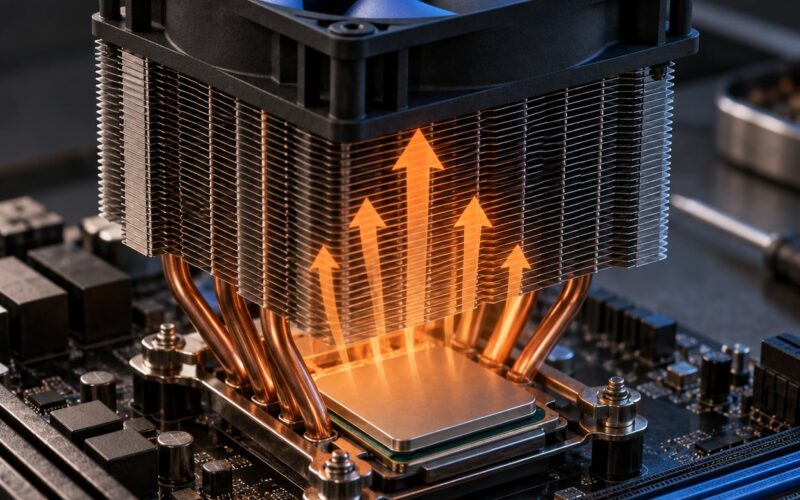
Beyond the die, three more variables change the result without the chip being different. Cooling matters: a better cooler can move the limit from thermal to electrical. Motherboard power delivery and the quality of the voltage regulator decide how much voltage droop and ripple the die actually sees, and both scale with load. Firmware decides how much of the die is used: adaptive voltage offsets, workload-based frequency offsets and boost algorithms all set the effective starting point before you touch anything.
Memory has its own layer. A memory subsystem that is unstable or badly tuned will corrupt a workload long before the core gives up, and a system that looks stable because the test is memory-light is telling you very little about the core.
Workload matters most of all. Heavy vector and matrix workloads pull far more current per cycle than scalar work, which is why parts that clock well in games can throttle hard in a render. A single number for “overclocking headroom” is always a number about a specific test.
How Manufacturers Test Chips Before Sale
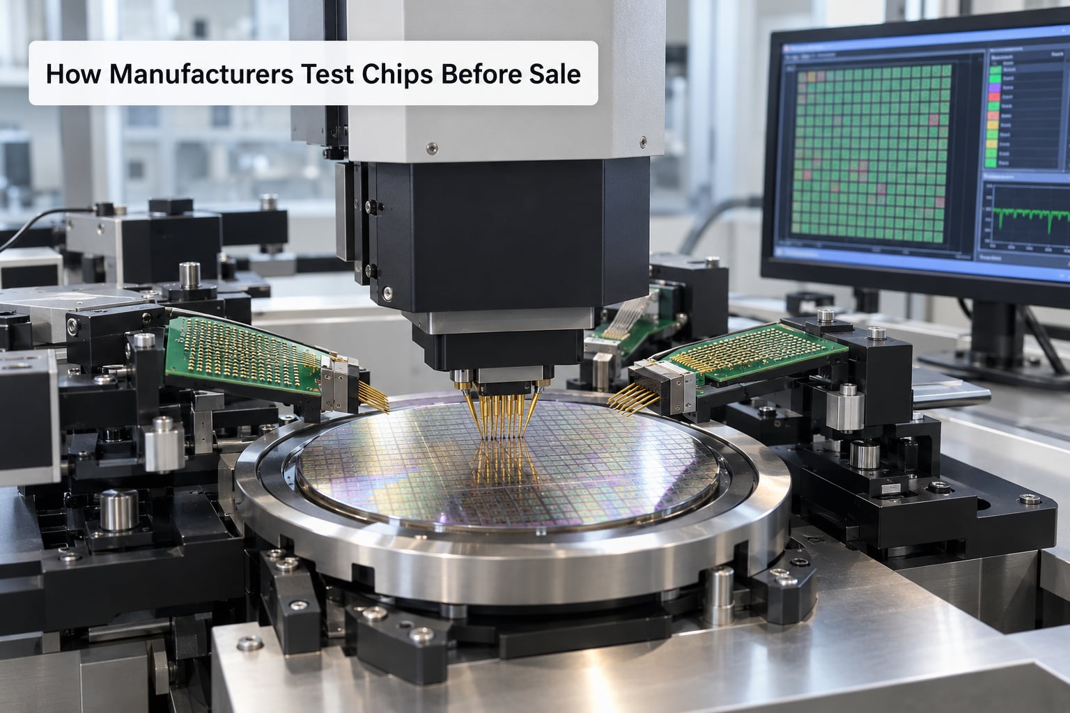
Testing starts where fabrication stops. At wafer sort, a probe card makes electrical contact with each die and a tester applies patterns while measuring timing, current and functional results. The measurement is fast, repetitive and automated, and it is the only economically viable place to reject millions of dies.
Frequency and voltage validation follows the functional screen. A part is stepped through a set of frequency points and voltage points, and the tester records where each unit stops passing. The relationship between voltage and sustainable frequency is usually drawn as a voltage-frequency curve, and the intersection of a die’s curve with a product’s required frequency is the binning decision in its most concrete form.
Temperature enters because timing margin depends on it. A test run at a cold junction is not a guarantee at a hot one, so parts destined for extended-temperature grades face harsher conditions, tighter guardband and more pattern sets than consumer parts. The guardband is the deliberate margin the designer leaves so a unit that passes still passes years later, after ageing.
Final test happens on the packaged part, on the board a customer will actually receive. It confirms the package, the interfaces and the fuse configuration, and it is where a lot code and date code get bound to the individual unit. Longer programs exist for parts that justify them: burn-in screens parts for server, automotive and industrial duty cycles specifically to shake out early-life failures, and no consumer processor gets one.
What comes out the other side is a maximum rated specification, not a measurement of your part’s ceiling. The datasheet number is a promise about the worst unit in the population meeting a defined test condition. It says nothing about the distribution above it, and it is not a prediction of what your unit will do.
How to Estimate Overclocking Headroom Safely
A useful estimate comes from reading, watching and stepping in that order. It costs an afternoon and avoids the two expensive mistakes, which are an unstable setting and a damaged part.
Start with what the part is guaranteed to do. Note the guaranteed clock, the supported voltage range if the vendor publishes one, the recommended memory speed and the recommended cooler. Also note the workload-dependent offsets. A part whose advertised clock already drops under heavy vector load has less room above that behaviour than the headline number suggests.
Watch temperatures before you change anything. Load the part the way you will actually use it, and record clock, package temperature, voltage and per-core behaviour together. A system that is already throttling under load has no headroom to give, whatever the numbers look like at idle. Silicon Lottery and other retailers grade chips by observed behaviour like this, and enthusiast reports of spread between units usually come from exactly this kind of logging.
Raise frequency in small increments and re-test each time. Moving by 25 to 50 MHz at a time, with a test long enough to be meaningful after each step, produces a real stability boundary instead of a guess. Test the workloads you care about rather than a synthetic loop, because a workload-light test can pass well past the point where a heavier one fails.
Treat voltage as the last variable, and change it conservatively. A modest increase can unlock a meaningful frequency step, but the margin you gain shrinks quickly and the cost rises fast. The mechanisms that matter are electromigration, where current causes metal atoms to migrate in the interconnect and eventually break a line, and threshold voltage shift, where a device’s switching voltage drifts under sustained bias and heat. Both accumulate over time rather than instantly, which is why a setting that passes a week of testing can still shorten a part’s life.
Know when to stop. If the frequency step you are chasing costs more cooling, power or board expense than the performance is worth, you have found the answer. Sooner or later headroom becomes a matter of diminishing returns, and the sensible result is a stable setting that you can run for years rather than a maximum that only holds for an hour.
Headroom for CPUs, GPUs, Memory, and Other ICs
Headroom means something slightly different depending on what is limiting the part, and the evaluation method changes with it.
On a processor, headroom is judged on sustained frequency across core counts and workload classes, with junction temperature and delivered voltage as the two limits. Because a die is held to its slowest path, gains usually come from a voltage step that lifts the whole curve, and they show up first in all-core behaviour rather than in single-thread figures.
On a graphics card, the board sets the power limit and the cooling, so the same die behaves differently in two chassis. The relevant variables are the power limit, the temperature limit, the memory error rate under load and whether the fitted memory was tested at the speed the card advertises. Memory error is the failure mode enthusiasts watch most closely, because it produces corrupt frames and silent computation errors long before the card says anything.
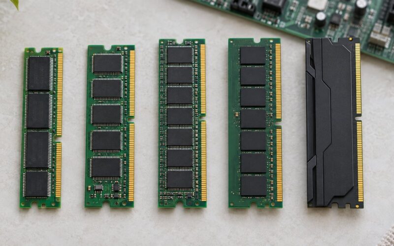
On memory, headroom is a timing-and-voltage curve, and the binning is often subtler. Modules are sorted for a speed grade, but a kit that passes a light benchmark may fail under sustained fill rates, and mixing kits of different bin inside one system is a common source of instability that looks like a core problem.
For FPGAs and specialised silicon, the story changes again. There the constraint is usually logic, routing and timing closure rather than thermal headroom, and the practical move is a different speed grade from the same design rather than a user-tunable frequency at all. Getting a faster grade means paying for the vendor to have qualified that configuration, which is why these parts see little enthusiast tuning.
Chip Binning and Overclocking Headroom Explained in Practice
Take a case where two dies from the same wafer land in different speed bins. The first meets the top grade and ships as a higher tier with a higher guaranteed boost clock; the second is slower and ships lower. Now push both. The higher-binned part usually has more room, because a die that reached a high frequency with room to spare started from a faster curve. But the relationship is a tendency, not a rule, and the lower-binned part can occasionally win because its extra gap came from a favourable leakage or voltage distribution rather than a lucky edge.
Swap in cooling and the result changes again. Give the lower-binned part a better cooler and a board with cleaner power delivery, and the limit can move from thermal to electrical, which often produces a larger practical gain than any silicon difference. The same die on a thin motherboard with two power stages and no heatsink contact will look like the worst sample you have ever owned, and it will say nothing about the silicon.
That is the practical summary: binning tells you what the part is guaranteed to be, headroom tells you what this part can be, and the gap between those two statements is decided by silicon, board, cooling and workload together.
Frequently Asked Questions
Does chip binning mean every chip has a different maximum speed?
No. Binning sorts dies into a limited number of defined grades, and a product name corresponds to one of those grades. Every part in a given bin is tested to the same requirement and warranted to the same specification. What varies between individual units is how much they exceed that requirement, and you can only find that out by testing the part yourself.
Is overclocking headroom guaranteed for chips with the same model number?
No, and this is worth being blunt about. A model number is a guarantee about a floor, not a promise about a ceiling. Two parts with identical model numbers can differ by several hundred MHz in sustained behaviour. A guaranteed specification is a contractual statement about minimum performance; headroom is a property of your particular unit, board and cooling.
Why can a lower-binned CPU overclock better than a higher-binned one?
Because the two tests measure different things. A speed grade comes from a frequency threshold, while a good overclock depends on the whole voltage-frequency curve, leakage, how the die was binned for power, and the board you use it on. A lower-binned part with an unusually flat curve can overtake a higher-binned part, especially once cooling stops being the limiting factor.
How much voltage increase is normally needed for extra performance?
Treat any figure as specific to a part rather than general. Small increases, on the order of tens of millivolts, often buy a meaningful frequency step, and the gain falls off quickly beyond that. Large increases buy little extra frequency while sharply accelerating electromigration and threshold voltage shift, which is why experienced tuners change voltage in small steps and re-test rather than jumping to a number copied from a forum.
Can overclocking reduce a processor’s expected lifespan?
It can, and the effect is a matter of accumulated stress rather than a sudden failure. Sustained voltage and heat drive electromigration in the interconnect and threshold voltage shift in the transistors, both of which degrade timing margin over time. A modest, cool, stable setting that is re-validated periodically is a very different proposition from a maximum that runs hot for months.
Does cooler memory or a stronger motherboard create more chip headroom?
Indirectly, yes. Neither changes the die, but memory that is stable and correctly tuned stops producing errors that masquerade as a weak core, and stronger voltage delivery means less droop and ripple, so the die sees the voltage you set. Better cooling removes the thermal ceiling. Once those two limits are gone, what remains is genuine silicon headroom, and that is what you cannot buy.
Conclusion: Start With Ratings, Then Test Carefully
Chip binning is a factory decision that turns one wafer’s spread of quality into a product ladder. Overclocking headroom is what remains above the guaranteed point for your particular unit, and it is decided by silicon, board, cooling and workload together.
So start with the ratings, treat them as the floor they are, and then measure your own part. Log temperatures and voltage under a real load before changing anything, step frequency up in small increments, and stop when the gains stop being worth the heat. That method finds the honest number for your chip instead of the one you hoped for.