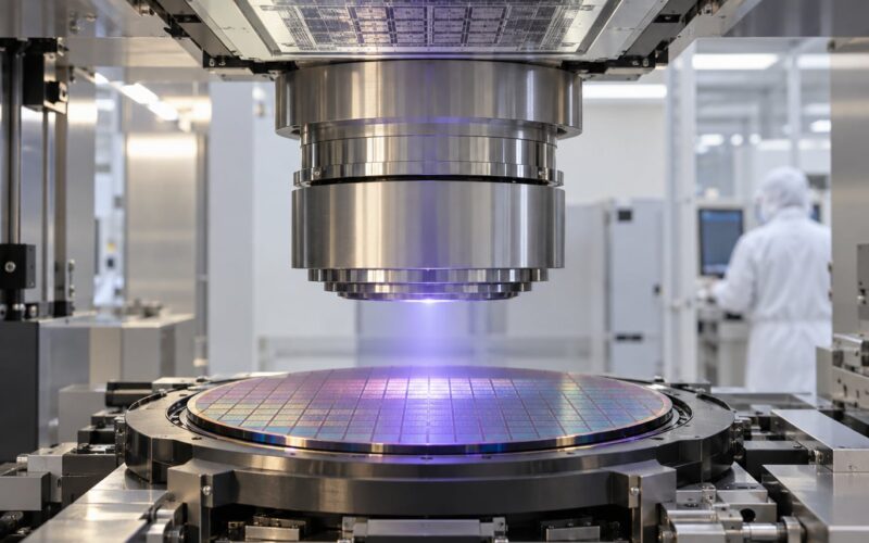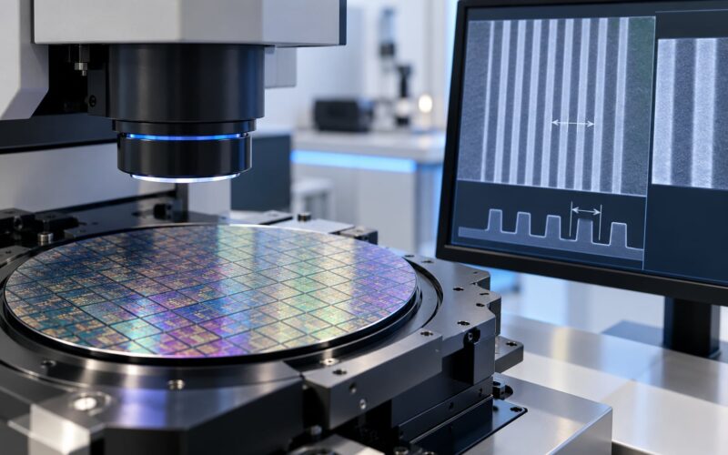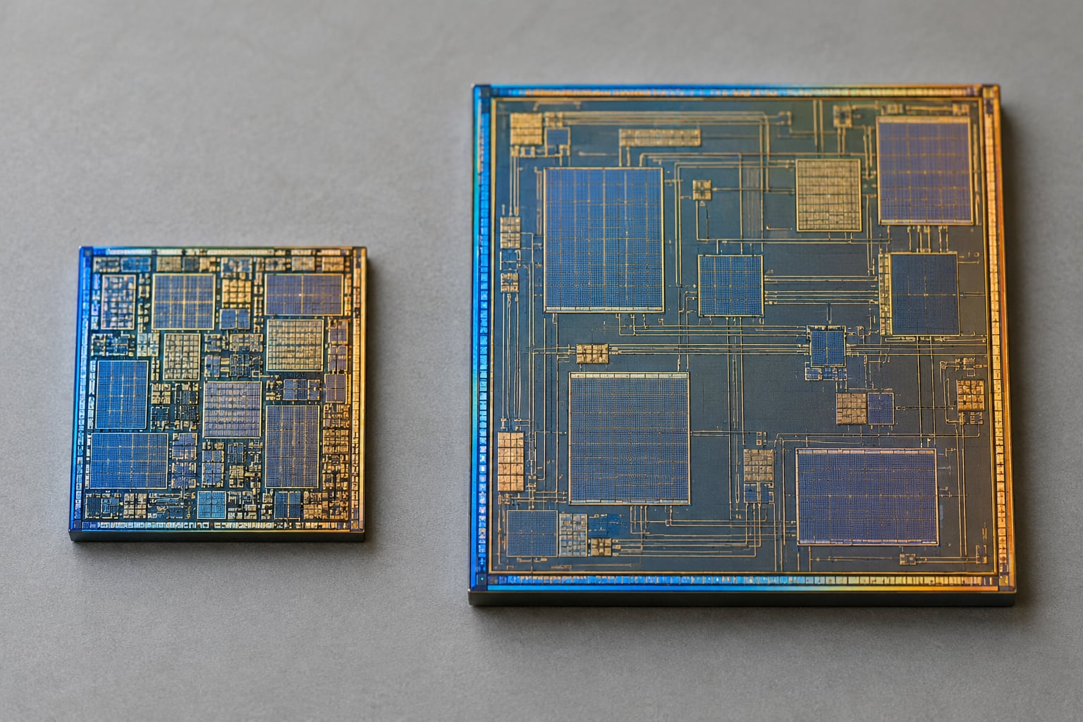
Choosing between the 3nm and 5nm process nodes comes down to one question: does the smaller node buy enough performance-per-watt or logic density to justify its higher cost and thinner design ecosystem? A 3nm design typically delivers roughly 10-15% more performance at the same power, or 25-30% less power at the same speed, over an optimized 5nm design — and about 1.6x the logic density. That gain is real but far smaller than the node names suggest, and that gap is exactly what this 3nm vs 5nm chip process comparison has to account for.
This guide is written for engineers, architects and technology planners who need a decision rather than a feature checklist. Current foundry reality matters more than the label: TSMC’s launch 3nm nodes (N3B, N3E) are still FinFET, while Samsung Foundry’s 3nm is gate-all-around nanosheet. Comparing a Samsung 3nm part against a TSMC 3nm part is not an apples-to-apples comparison, and comparing either against 5nm by name alone tells you very little.
Table of Contents
- 3nm vs 5nm Chip Process Comparison at a Glance
- What Is the Difference Between 3nm and 5nm?
- Why node names stopped being physical sizes
- Performance and Power Efficiency
- Density, Area, and Design Flexibility
- Manufacturing Cost, Yield, and Time-to-Market
- EDA, IP, and Design Ecosystem
- What to confirm before choosing 3nm or 5nm
- Which Should You Choose?
- Frequently Asked Questions
- Is a 3nm chip twice as fast as a 5nm chip?
- Does 3nm always use less power than 5nm?
- Why do different foundries use different process names for similar transistor sizes?
- Is 5nm suitable for AI and high-performance computing chips?
- Which is cheaper to manufacture, 3nm or 5nm?
- Do smaller transistors always produce a smaller chip?
- Conclusion
3nm vs 5nm Chip Process Comparison at a Glance
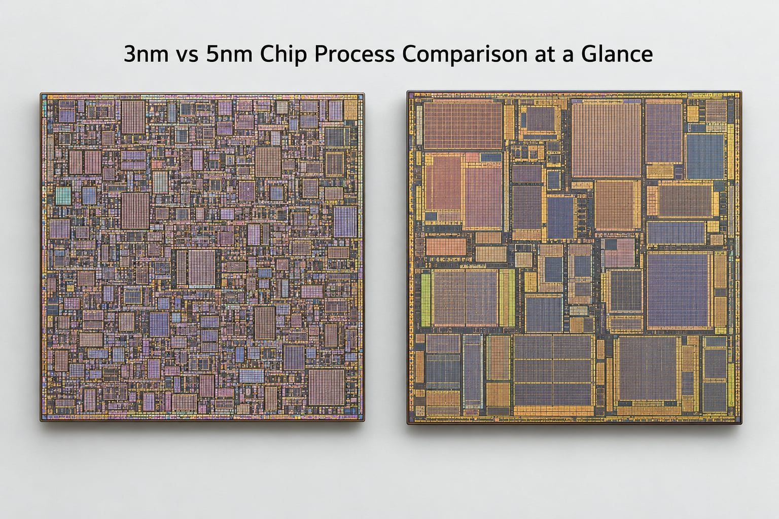
The table below is the fastest way to see where the two nodes separate. Every figure is a typical range from published foundry process data, not a guarantee — real results depend on the specific variant, the standard-cell library, the voltage and frequency point, and how well the design was optimized for the node.
| Criterion | 3nm | 5nm |
|---|---|---|
| Transistor architecture | FinFET at N3B/N3E; nanosheet gate-all-around in later nodes | FinFET (nanosheet on some later variants) |
| Contacted poly pitch | About 48 nm | About 51 nm |
| Metal pitch | About 22 nm | About 30 nm |
| Logic density vs the other node | About 1.6x the density of 5nm | Baseline |
| Performance at iso-power | About 10-15% higher clock than an optimized 5nm design | Baseline |
| Power at iso-performance | About 25-30% lower power, or roughly 25-35% on some process claims | Baseline |
| SRAM scaling | Weaker than logic scaling; bitcell gains trail logic density gains | Closer to a straight geometry shrink |
| Design (NRE) effort | Substantially higher; large design teams and long schedules | Lower; mature flows and wide IP availability |
| Time to volume | Longer; newer node, more immature defect learning | Shorter; well-characterised process |
| Ecosystem maturity | Newer PDKs, fewer characterised IP blocks | Broad IP, EDA certification and reference flows |
| Best fit | Flagship SoCs, HPC, leading-edge AI accelerators | Broad product lines, cost-sensitive volume, mature architectures |
One caveat belongs right at the top: nominal node names are not comparable across foundries. TSMC, Samsung, Intel and SMIC all label generations differently, and a “7nm” from one vendor can be smaller or larger than a “7nm” from another. Judge the process by its contacted poly pitch, metal pitch, density figures and design rules — that is what this comparison actually measures.
What Is the Difference Between 3nm and 5nm?
A process node is not a single dimension. It is a bundle of changes shipped together: the transistor structure, the materials, the interconnect stack, the design rules and the standard-cell libraries. Moving from 5nm to 3nm shrinks the contacted poly pitch from about 51nm to about 48nm and the metal pitch from about 30nm to about 22nm, which is what drives the density increase.
That metal pitch reduction is the quiet story. Logic transistors got smaller, but the wires connecting them did not shrink proportionally, and interconnect resistance and capacitance now account for a large share of delay and dynamic power in advanced logic. RC delay in the middle-of-line and back-end-of-line structures is the main reason a node shrink that buys 1.6x density does not deliver 1.6x speed.
SRAM follows its own path. Logic cells scale close to their ideal pitch, while SRAM bitcells carry access transistors and routing that resist the same shrink. Register files and cache therefore gain less than the headline logic density figure, which matters directly to AI accelerators and large-core CPUs whose performance leans on on-chip memory bandwidth.
Why node names stopped being physical sizes
Below roughly 90nm, node names began tracking a mix of features rather than any single measurable dimension, and above about 20nm they stopped tracking geometry altogether. Fabs market generations, not nanometers. Intel labels its nodes Intel 7, Intel 4 and Intel 18A; TSMC uses N3E and N4P; Samsung uses SFG and its own generational numbering. The digits are shorthand for a process generation, which is why nobody serious compares nodes by the number alone.
Architecture is the second difference. A FinFET wraps the channel in a thin vertical fin with a gate on three sides. A gate-all-around nanosheet uses a thin stacked sheet surrounded by the gate on all four sides, which improves electrostatic control of the channel and lowers voltage needed to drive it. That control is what makes low-voltage, high-performance operation possible at the leading edge — and it is exactly what TSMC’s first FinFET-based 3nm nodes do not have yet.
Performance and Power Efficiency
The honest performance answer: a 3nm chip is not twice as fast as a 5nm chip, and it is not automatically quieter-running either. The gain is workload- and voltage-dependent, and it is measured against an already well-optimized 5nm baseline.
| What a vendor claims | What you measure on silicon |
|---|---|
| Higher clock at the same power budget | About 10-15% higher sustained frequency when thermal limits and library choices are held equal |
| Lower power at the same speed | About 25-30% lower total power, dominated by dynamic switching reduction at iso-performance |
| More transistors on the same die | About 1.6x logic density, but less than 1.6x in cache and analog blocks |
| Better performance per watt | Real, and the most defensible reason to pay for a node shrink on battery-powered products |
At iso-power, the 3nm part runs faster and does more work per joule. That is where the efficiency story is cleanest, because the baseline is fixed at the same power ceiling and the gain comes from lower voltage per switching event.
At iso-performance, the 3nm part burns less power for the same throughput. Leakage improves too, but less dramatically than dynamic power, and designs that hold high voltage for throughput gains claw back some of the nominal advantage.
A 3nm design can deliver almost nothing over a good 5nm design in three common situations: the workload is memory-bound rather than compute-bound, the product ships in a large volume where cost per unit dominates, or the 5nm baseline was itself well optimized with aggressive floorplanning and multi-corner timing closure. Buyer’s-eye discussions in hardware forums make a related point: efficiency differences between generations are partly masked by the vendor’s own clock and power-policy choices, so the node shrink is only part of what you are measuring.
Density, Area, and Design Flexibility
Density is the strongest argument for 3nm, and it is where the 1.6x figure comes from. Where a product is constrained by die area, power envelope or cooling budget, 3nm lets you place meaningfully more logic in the same footprint.
Die size does not shrink 1.6x, though. Analog blocks, I/O rings, PHY and SerDes circuitry, and large SRAM arrays scale far less than standard cells, so a design that is mostly logic can shrink close to the density number while an I/O-heavy part barely moves. Smaller transistors also raise the cost of a fix in the back end: a defect that would have killed a large die in an older node may now land in a smaller, cheaper die — but at a higher ratio of defective parts to good ones during the ramp.
Design flexibility improves where cells are compute-dense, such as AI accelerator datapaths, GPU compute units and CPU cores. It does not automatically improve for memory-heavy logic, and register-file-heavy designs should verify SRAM bitcell scaling in the target process rather than assume it tracks logic density.
Manufacturing Cost, Yield, and Time-to-Market
3nm costs more at every step. The wafer itself starts at a higher price, and each wafer step requires more EUV lithography passes, tighter overlay control and more advanced metrology, which pushes yield learning harder on a node with fewer good dies to average the fixed cost over.
Design cost is where the gap widens most. Leading-edge node design runs into the hundreds of millions of dollars, and the 3nm figure sits substantially above 5nm — the extra spend buys verification coverage, physical signoff work, IP licensing and engineering time on a node where the escape routes and reuse options are fewer. That cost lands on a project whether or not the design succeeds, which is why smaller teams usually pick the more mature node.
Yield and time-to-volume follow the same curve. A 5nm design is running on a process with years of accumulated defect learning, characterised libraries and proven signoff flows. A 3nm design is still accumulating that data, so schedules slip and the first products are more likely to be large, high-value parts where silicon cost is a small share of the system.
The better cost metric is cost per useful performance, not cost per nanometer. If the same product function runs at 25% lower energy on 3nm, the power bill, the battery capacity and the cooling budget all scale down with it. For a data center accelerator running continuously, that number decides the node. For a low-volume consumer part, it rarely does.
EDA, IP, and Design Ecosystem
The ecosystem gap is the least glamorous reason to stay at 5nm, and often the strongest. A mature node has standard-cell libraries with deep timing characterisation, SRAM compilers with proven yield, analog and mixed-signal IP that has already been taped out and qualified, and EDA flows that most design teams have run dozens of times. A newer node has fewer of each, and each gap is engineering time you have to pay for.
IP availability decides a lot of schedules. If the SerDes, the PCIe PHY or the DDR interface you need has not been certified on the target node, you are looking at a block-level redesign while the rest of the chip is already being taped out. Chiplet-based designs help here, because you can hold an interface die at 5nm and pair it with a 3nm compute die in an advanced package — which also trades some interconnect efficiency for schedule and yield.
What to confirm before choosing 3nm or 5nm
- Which exact variant you are targeting, and its specific process design rather than the family name
- Contacted poly pitch, metal pitch and published density figures for that variant
- Which of your required IP blocks are already available, signed off and certified
- SRAM bitcell scaling, if your design is register-file or cache heavy
- Analog and I/O area as a share of the die, since that is the part that scales worst
- Qualification, reliability and reliability-monitoring requirements for your end market
- Whether advanced packaging capacity is part of your plan, and who supplies it
Which Should You Choose?
The decision framework is simpler than the node numbers suggest: pick 3nm when your product’s power envelope, die area or sustained throughput is a binding constraint that only a node shrink can relieve. Pick 5nm when maturity, cost predictability and schedule matter more than the last 15% of performance.
| Product | Recommended node | Reason |
|---|---|---|
| Flagship smartphone SoC | 3nm when volume justifies it, otherwise 5nm (or the newest mature node) | Battery and thermals are the constraint; gains are visible only at the top of the range |
| AI accelerator / GPU | 3nm | Datapath density and memory-adjacent logic reward density gains |
| Data center CPU | 3nm for HPC parts; chiplets let the I/O stay at an older node | Energy per rack unit dominates the cost model |
| Automotive MCU / PMIC / RF | 5nm or older, or even mature nodes | Qualification, longevity and cost outweigh leading-edge density |
| Cost-sensitive high-volume device | 5nm | Per-unit cost and supply predictability dominate |
3nm earns its premium in leading-edge AI, high-performance computing and flagship mobile silicon, where the product is sold on sustained performance and where the incremental cost per unit is small relative to the system value.
5nm is no longer an old node. For broad product lines, mature architectures, cost-sensitive volume and teams without deep leading-edge experience, it is the value node: mature PDKs, wide IP, predictable schedules and a much lower NRE. Plenty of 5nm designs are the right answer today.
The first decision a project team should make is not which node to pick. It is identifying which constraint actually limits the product — power, area, throughput or cost per unit — and checking whether that constraint is set by the process or by the architecture. Fix the architecture first, then choose the node.
Frequently Asked Questions
Is a 3nm chip twice as fast as a 5nm chip?
No. Moving from an optimized 5nm design to 3nm typically delivers about 10-15% higher performance at the same power budget, or roughly 25-30% lower power at the same speed. The larger gain is usually in logic density, around 1.6x, which lets designers add more logic to the same die rather than running existing logic twice as fast.
Does 3nm always use less power than 5nm?
No. Lower power is measured at the same performance point. A 3nm design pushed to a higher clock and higher voltage can draw more power than a 5nm part running at a lower frequency. That is why the meaningful figures are iso-performance and iso-power numbers, and why thermal limits can erase much of the advantage in a thin, passively cooled device.
Why do different foundries use different process names for similar transistor sizes?
Because the names are marketing generations, not physical measurements. Since features stopped correlating with any single dimension, each foundry branded its own numbering scheme, so Intel 7, TSMC N4 and Samsung SFG describe generations rather than comparable sizes. Compare processes using contacted poly pitch, metal pitch, transistor density and the design rules that come with them.
Is 5nm suitable for AI and high-performance computing chips?
Yes, particularly for designs where cost per unit matters and the product does not need the last 15% of performance. 5nm offers mature libraries, wide IP availability and proven flows, which often lets a team reach production sooner. Many AI accelerators also split compute and I/O across chiplets, keeping I/O on 5nm while a newer node handles the datapath.
Which is cheaper to manufacture, 3nm or 5nm?
5nm, in every meaningful sense. Wafers cost more at 3nm, process steps and equipment intensity are higher, yields are still ramping, and design effort runs into the hundreds of millions of dollars against a somewhat lower figure at 5nm. The exception is when lower power or greater density cuts a much larger system cost, such as cooling or battery capacity.
Do smaller transistors always produce a smaller chip?
No. Logic density gains of about 1.6x do not translate into a 1.6x smaller die. Analog blocks, I/O rings, PHYs and SRAM arrays scale far less than standard cells, so an I/O-heavy part shrinks much less than a logic-heavy one. Wire pitch also improves more slowly than the device pitch, which limits how much of the density gain a real design can actually use.
Conclusion
Compare the process design and your product’s power, performance and area targets, not the node names. A 3nm vs 5nm chip process comparison is really a comparison of contacted poly pitch, metal pitch, density, libraries and interconnect — the label only tells you which generation a foundry is marketing.
Use 3nm when its advanced capabilities materially improve the product: a flagship mobile SoC fighting a thermal envelope, an AI accelerator whose datapath needs the density, an HPC part where energy per rack unit dominates the economics. Choose 5nm when ecosystem maturity, predictable cost and schedule execution matter more.
Before committing, benchmark the candidate PDK and library implementations with your own representative design. Implement a slice of the architecture on both nodes and measure where the time and power actually go. That data settles the argument faster than any roadmap.