A FinFET is a three-dimensional transistor in which the gate wraps around a thin, vertically standing silicon fin on three sides instead of controlling the channel only from above. That extra gate contact is what lets chipmakers keep shrinking transistors, cutting leakage and power while raising drive current.
So, in plain terms, what finfet transistors are and how do they work? This guide covers the structure, the switching mechanism, the fabrication sequence, and the honest trade-offs that rarely make it into consumer-facing explanations.
Table of Contents
- What FinFET Transistors Are
- The parts that matter
- A quick history correction
- Why Semiconductor Manufacturers Use FinFETs
- What FinFET Transistors Are and How They Work
- How a FinFET is fabricated
- The electrical switching cycle
- Why a FinFET has multiple fins
- How FinFETs build a logic gate
- How a FinFET Differs from a Planar Transistor
- Types of FinFET Designs
- How FinFETs Are Used in Modern Chips
- What Are the Advantages and Tradeoffs of FinFETs?
- What FinFETs genuinely improved
- What FinFETs made harder
- Frequently Asked Questions
- Are FinFETs better than planar transistors?
- What is the gate in a FinFET?
- Why does a FinFET have multiple fins?
- What process nodes first used FinFETs?
- Does a FinFET improve speed or mainly reduce power?
- How are FinFETs different from gate-all-around transistors?
- The Bottom Line
What FinFET Transistors Are
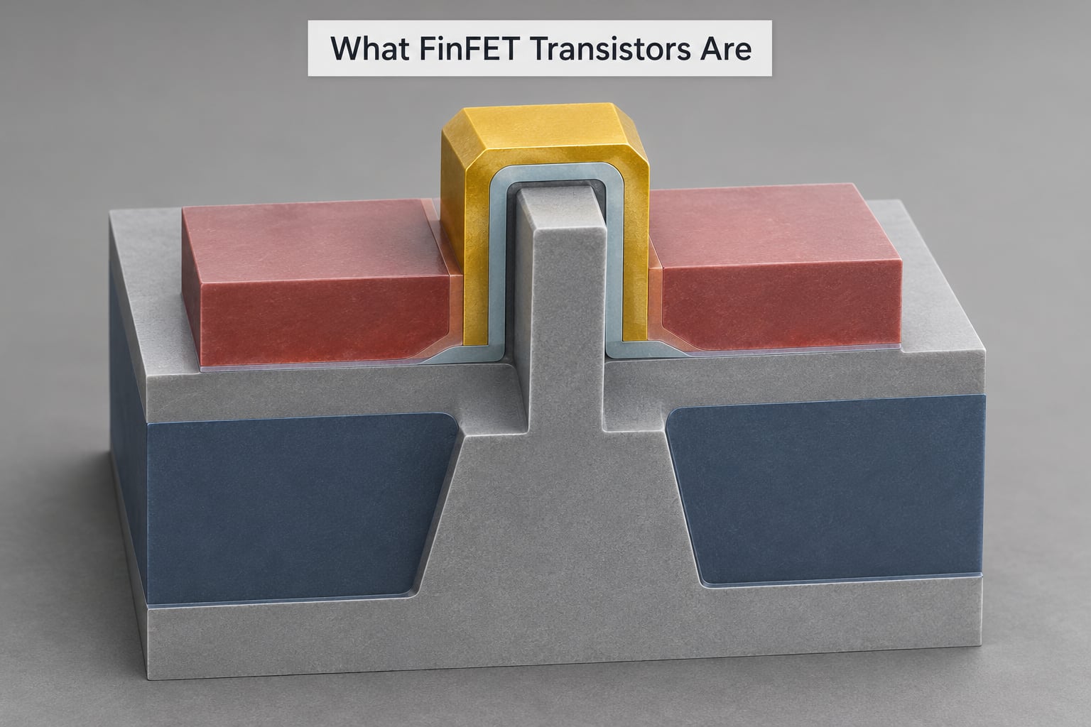
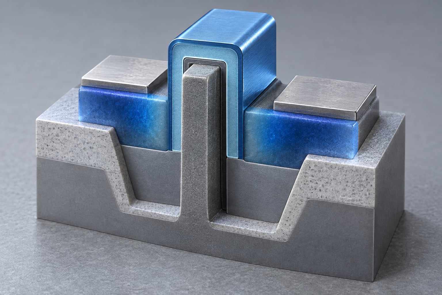
A FinFET (fin field-effect transistor) is a three-dimensional transistor in which the gate wraps around a thin vertical silicon fin on three sides, controlling the channel from the top and both lateral faces instead of only from above as a planar MOSFET does.
The name is literal. The channel that carries current between source and drain is shaped like a fin standing up from the silicon surface, usually 20 to 50 nanometres tall and only about 6 to 7 nanometres wide. Because the fin is tall and narrow, there is far more channel surface per unit of die area than a flat channel provides.
Intel coined the useful term “tri-gate” for this geometry: gate on top, gate on the left side, gate on the right side. When the fin is made slightly wider than it is tall, the top gate is weak compared with the two side gates and engineers use terms such as “omega gate” or “multi-gate” instead.
The parts that matter
Two dimensions describe a FinFET for most purposes. Fin height is set by how far the fin stands above the surrounding isolation, and it is the dominant term in drive current. Fin width is a lithographic dimension that a designer cannot vary freely for a given process.
Because of that, FinFET designers specify a fin count rather than an arbitrary width. The effective channel width is roughly Weff ≈ 2 × Hfin + Wfin — two side surfaces plus one top surface. A device with four 30 nm-tall fins and a 6 nm fin width has an effective width near 66 nm, and there is no design rule that lets you ask for 71 nm instead.
A quick history correction
FinFETs are often described as “proposed in 2011.” That is wrong. The fin-shaped channel was published in the late 1980s and around 1990 by Digh Hisamoto and colleagues at Hitachi, who were studying how to control leakage in ever shorter channels. What happened in 2011 was manufacturing: Intel put FinFETs into high-volume production at its 22nm node, in the Ivy Bridge generation.
The idea was roughly two decades old before it shipped. That gap between invention and production is normal in semiconductors, and it is worth keeping in mind whenever a new transistor architecture is announced as finished.
Why Semiconductor Manufacturers Use FinFETs
Planar transistors stopped scaling because of a family of problems collectively called short-channel effects. Once the channel is only a few tens of nanometres long, the drain’s electric field starts interfering with the gate’s ability to hold the transistor off, and nothing the gate does can be kept local.
The symptoms show up one at a time and then all at once:
- Off-state leakage: a transistor that should block current lets a trickle through, and an idle chip still burns power. On a phone this is battery life, and in a data centre it is a rack of heat.
- DIBL (drain-induced barrier lowering): voltage on the drain lowers the barrier the gate must overcome, so a “0” state weakens as the supply voltage rises.
- Threshold voltage roll-off: below a certain channel length the gate loses authority and the switching point collapses.
- Drain punch-through and channel length modulation: the depleted regions under source and drain grow until they touch or the output current depends on output voltage.
- Velocity saturation: carriers hit a speed ceiling, so shrinking further stops buying current.
- Surface scattering: carriers in the thin inversion layer under the gate collide with the interface and lose mobility.
There was a second problem, more mundane. The gate insulator could not keep shrinking. Once the silicon dioxide layer approached a couple of nanometres, electrons tunnelled straight through it, so the gate leaked current into the channel whether or not the device was switching.
Modern nodes solved that with high-k dielectric materials such as hafnium oxide, which are physically thicker but electrically behave like a very thin oxide, paired with a metal gate. FinFET structure is the parallel solution: if you cannot squeeze the gate closer to the channel horizontally, wrap it around the channel instead.
Wrapping the gate improves electrostatic control because the gate-to-channel distance is short on three surfaces rather than one. At a 300 K, the thermal limit on subthreshold slope is about 60 mV per decade of current; strained planar devices in the 32 nm era were already pushing past 80 mV per decade, while FinFETs recovered much of that margin.
What FinFET Transistors Are and How They Work
Two separate questions hide inside “how does a FinFET work”: how the device is built, and what happens electrically when it switches. Both are worth walking through.
How a FinFET is fabricated
- Grow or etch the fin. On a bulk substrate, a fin is formed by patterning a hard mask and etching into the silicon. On an SOI wafer, the buried oxide stops the etch and the fin is simply the remaining silicon above it.
- Isolate the neighbouring fins. Shallow trench isolation (STI) fills the trenches and defines how much space each fin keeps from its neighbour. This fin-to-fin spacing is the number that later limits how far the node can shrink.
- Deposit the gate stack. A thin high-k dielectric is grown or deposited conformally over the fin, followed by a metal gate layer, so the gate covers the top and both sides. In practice a sacrificial gate nitride stands in first, and the real gate is formed later.
- Form source and drain. Spacers are added, and source and drain regions are created by epitaxial growth and doping at each end of the fin, so carriers are injected cleanly into the channel.
- Open contacts. The dummy gate is removed, the high-k and metal gate are patterned, and tungsten or cobalt contacts connect source, drain and gate to the metal stack above.
The electrical switching cycle
With no gate voltage, the channel is depleted of free carriers and the device blocks current apart from a small subthreshold leak. Raise the gate voltage above the threshold and the electric field inverts the channel: electrons in an n-type FinFET (or holes in a p-type one) form a continuous layer along the fin, bridging source and drain. Current flows.
Drop the gate voltage and that inversion layer collapses into isolated pockets of charge, and current stops again. A FinFET is a voltage-controlled switch, and every digital operation in a processor is millions of these switches moving between those two states.
Why a FinFET has multiple fins
A common question on r/AskElectronics is whether a multi-fin device is just several transistors in one package. It is not. All fins in a standard device share one gate electrode and one source-drain pair, so the gate switches all of them together as a single transistor. More fins simply means more channel width, and therefore more drive current for the same footprint.
The industry shifted toward independent-gate devices in later FinFET generations, where each fin can be driven separately. That is useful for powering down the unused fins of a wide device, cutting leakage in standby, and it also gives designers a way to trade drive current for capacitance inside the same standard cell.
How FinFETs build a logic gate
A CMOS inverter needs one n-type and one p-type FinFET. Pull the gate high and the n-type conducts while the p-type blocks, giving a logic zero; pull it low and the roles swap, giving a logic one. Every NAND, adder, register file and cache bit in a modern processor is an enormous number of these pairs, sized by fin count and stacked in standard cell rows.
How a FinFET Differs from a Planar Transistor
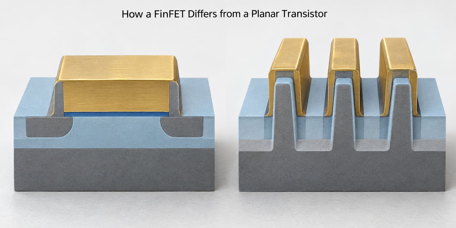
The difference comes down to geometry, and everything else follows from geometry. A planar transistor has a horizontal channel sitting on the silicon surface with the gate above it; a FinFET has vertical fins with the gate hugging three sides of each one.
| Property | Planar MOSFET | FinFET | Gate-all-around (GAAFET) |
|---|---|---|---|
| Channel geometry | Flat, horizontal, on the surface | Vertical fin, tall and narrow | Stacked nanosheet wrapped on four sides |
| Gate control surfaces | One (top) | Three (tri-gate) | Four (gate-all-around) |
| Off-state leakage | High at scale, worsens with drain voltage | Low, strongly suppressed | Lowest, fin-like control with more drive |
| Drive current per unit area | Limited by a thin surface channel | Higher, more channel surface per footprint | Higher still |
| Designer width control | Continuous width, easy to tune | Quantised by fin count and fin height | Quantised by sheet width and stack count |
| Practical scaling limit | Reached around the 28 nm generation | Fin pitch and contact pitch | Sheet pitch and inner spacer width |
| Shipping today | Legacy and analog, mostly | 16 nm through 7 nm and 5 nm class, still offered | 3 nm class and below on leading nodes |
Planar designs are not dead. Analog and mixed-signal blocks, image sensors, power devices and mature I/O still use planar or deep-trench isolated transistors, partly because continuous width control makes analog matching far easier, and partly because those nodes are cheaper to build.
Types of FinFET Designs
Most production chips use one family, but the literature and some foundry options cover a few variants worth distinguishing.
- Bulk FinFET (the industry standard tri-gate): fins etched directly into a silicon wafer, with STI between neighbours. This is what Intel shipped at 22nm and what TSMC used from 16nm onward.
- Double-gate FinFET: a SOI-based variant where the fin is thin enough that the two side gates do most of the work. It dates from the same early research wave and shows up in academic work more than in shipping silicon.
- Fully depleted FinFET: the fin is made thin enough that it carries no mobile charge in its own body when the device is off, so the gate alone determines whether current flows. This is the cleanest electrostatic behaviour of the family and is related to the fully depleted silicon-on-insulator idea.
- Independent-gate FinFET: each fin gets its own gate contact, allowing individual fins to be throttled or powered down. Adopted in later FinFET nodes for leakage control in memory and logic.
One thing these all share is that the channel is a fin. Gate-all-around devices are a different family, even when people use the words loosely: the channel there is a stacked nanosheet surrounded on all four sides, and the fin is a stepping stone rather than the destination.
How FinFETs Are Used in Modern Chips
FinFET is what carried the industry through the entire smartphone era and most of the current data-centre generation. Examples include Apple’s A11 and later mobile application processors on TSMC’s 16nm and 10nm FinFET nodes, Qualcomm Snapdragon parts from the 10nm generation onward, AMD’s Zen 2 through Zen 5 on TSMC 7nm, 5nm and 4nm, and NVIDIA’s Ampere and Ada GPU families on a customised 4N FinFET derivative of TSMC 5nm.
Intel’s Alder Lake and Sapphire Rapids parts sit on its 10nm and 7nm FinFET processes, and the same geometry underpins SRAM bitcells. Shrinking a bitcell in height is what packs more cache into the same die, which is why memory arrays gained from the three-dimensional channel as much as logic did.
Node names need care, and readers regularly misread them. “7nm” no longer describes any measured feature length; these labels are marketing generations, and two foundries’ 7nm nodes differ substantially in transistor density. TSMC’s N3 is its FinFlex generation, where a chip designer can choose between FinFET and gate-all-around implementations on what is broadly the same platform. Samsung moved to its 3GAE gate-all-around at 3nm, and Intel introduced RibbonFET with backside power delivery at 18A. So the honest answer to “is 3nm FinFET?” is: it depends on which foundry, and node names will not tell you.
And to “is a 1nm transistor possible?” — yes, in the sense that nodes labelled 1nm and 2nm are shipping or in production. Nothing physical shrank to that dimension. The naming reflects density improvements from a combination of FinFET and gate-all-around structures, EUV lithography and better interconnect.
What Are the Advantages and Tradeoffs of FinFETs?
FinFET delivered on the leakage and scaling promises. It also created new problems that the marketing rarely mentions.
What FinFETs genuinely improved
- Off-state leakage: three-sided gate control lets a lower threshold voltage be used for the same leakage, which means a lower supply voltage for the same performance.
- Drive current and speed: more channel surface per unit area delivers higher current density and faster switching than planar CMOS at the same node.
- Density: fins pack more transistors into the same footprint, and the vertical channel uses die area that a flat device cannot.
- Power per operation: dropping the supply from roughly 0.9 V to roughly 0.8 V alone cuts dynamic power by about a fifth, since dynamic power scales with voltage squared.
What FinFETs made harder
Dynamic power did not disappear. Adding a third gate surface increases gate capacitance, and the Miller effect between gate and channel got worse, so part of the leakage saving was handed back as switching energy. Semiconductor Engineering has covered this honestly, and it is the main reason people say FinFET bought performance, not efficiency.
Fin pitch is the wall. As fins sit closer together, the STI between them gets narrower and harder to fill without voids, and the source and drain contacts begin to crowd each other. Below a certain point the contact pitch, not the fin, sets how tightly transistors can pack.
Designers lost a knob they had with planar devices. Width is quantised into whole fins, which is awkward for analog and mixed-signal blocks that need finely trimmed ratios; porting a design between foundries means matching their specific fin height and fin count options rather than resizing freely.
Heat has a narrower escape route. The conducting channel now runs vertically through the device and releases heat into the surrounding silicon, so self-heating is harder to remove, and layout rules on neighbouring structures get tighter as a result.
And the cost is real. Three-dimensional patterning, epitaxial source and drain, gate-all-around spacer work and multi-patterning steps push a leading-edge wafer through far more mask layers than a planar node did. That is the pressure behind the industry shift to gate-all-around: it keeps the gate wrapped where the electrostatic benefits are, while giving the channel more width for the same footprint.
Frequently Asked Questions
Are FinFETs better than planar transistors?
Better at what matters most: controlling the channel at small sizes. The wrapped gate suppresses off-state leakage and short-channel effects, delivers higher drive current, and lets chips run at lower supply voltages. Planar transistors still win for analog and mixed-signal blocks, where continuously adjustable channel width is valuable, and for mature, low-cost nodes where the extra patterning steps do not pay for themselves.
What is the gate in a FinFET?
The gate is the metal electrode wrapped around the fin on three sides, separated from the silicon by a very thin high-k dielectric. Its job is to set the threshold voltage: applying a voltage strong enough pulls carriers into the channel to turn the device on, and removing it depletes the channel to turn the device off. Because the gate touches three surfaces, it holds the channel more firmly than a gate sitting only on top.
Why does a FinFET have multiple fins?
All fins in a standard device share one gate and one source-drain pair, so they act as a single transistor rather than separate ones. The reason for several fins is width: each fin adds channel surface, which adds drive current, and drive current is what lets a gate charge and discharge its load quickly. Later generations gave each fin its own gate so unused fins could be powered down independently.
What process nodes first used FinFETs?
Intel was first to ship them in volume, at its 22nm node in 2011 with the Ivy Bridge generation. TSMC followed at 16nm in 2014, then 10nm, 7nm, 5nm and, on the FinFlex generation, 3nm. Samsung used FinFET from 14nm to 4nm before switching to gate-all-around at 3nm, and Intel moved from FinFET to RibbonFET at 18A.
Does a FinFET improve speed or mainly reduce power?
Both, but the honest emphasis is speed plus flexibility. The wrapped gate raised drive current and cut switching time, which allowed a lower supply voltage for the same performance, and that lower voltage is where most of the power saving came from. Static leakage also fell. Dynamic power did not fall proportionally, because the extra gate surface raised gate capacitance.
How are FinFETs different from gate-all-around transistors?
A FinFET controls a vertical fin from three sides, so the top gate is weaker than the two side gates. A gate-all-around transistor, often called a GAAFET or nanosheet FET, wraps a thin stacked sheet of silicon on all four sides, giving more uniform control and more channel width per unit of footprint. Most shipping 7nm and 5nm parts use FinFET; leading 3nm and 2nm parts increasingly use gate-all-around.
The Bottom Line
Start with the geometry and everything else follows. A FinFET is a transistor whose channel stands up as a thin fin so the gate can wrap around it on three sides, giving much tighter electrostatic control than a flat channel ever could.
If you are evaluating a chip, stop treating the node name as a measurement. Ask which architecture the die uses, because at 3nm and below the answer may be FinFET, gate-all-around, or a mix of both on the same platform.