Dennard scaling is a law from a 1974 IEEE paper that says transistor dimensions, supply voltage and doping can be shrunk together so that power per unit area stays constant while the transistor gets faster. For three decades that let chips double their transistor count every generation without a thermal penalty, and it is the reason clock speeds climbed for so long.
If you have read about Moore’s law and wondered why processors stopped getting much faster around the middle of the 2000s, this is the physics behind that story. Below is the rule set, a worked numeric example, the reasons it broke, and what replaced it.
One shortcut for the whole topic: Moore’s law counted transistors. Dennard scaling explained what happened to power when those transistors got smaller, and why making them smaller stayed affordable in the first place.
Table of Contents
- Dennard Scaling Explained: What It Is and Why It Mattered
- What a transistor needs before scaling makes sense
- How Does Dennard Scaling Change Transistor Performance?
- Dennard’s three scaling rules
- A worked example: a 5 micrometre transistor scaled by K = 5
- Constant-field versus fixed-voltage scaling
- How Dennard Scaling Explained the Growth of Chip Density
- What Is the Difference Between Dennard Scaling and Moore’s Law?
- Why Did Dennard Scaling Eventually End?
- Five reasons the law stopped holding
- What Technologies Replaced Dennard Scaling?
- How Does Dennard Scaling Relate to Modern Semiconductor Manufacturing?
- Frequently Asked Questions
- What does Dennard scaling mean?
- Why was Dennard scaling important for CPUs?
- Is Dennard scaling the same as Moore’s law?
- When did Dennard scaling stop working effectively?
- What replaced Dennard scaling in modern chips?
- Does a smaller process node automatically mean better performance?
- Conclusion: Start With the Scaling Principle
Dennard Scaling Explained: What It Is and Why It Mattered
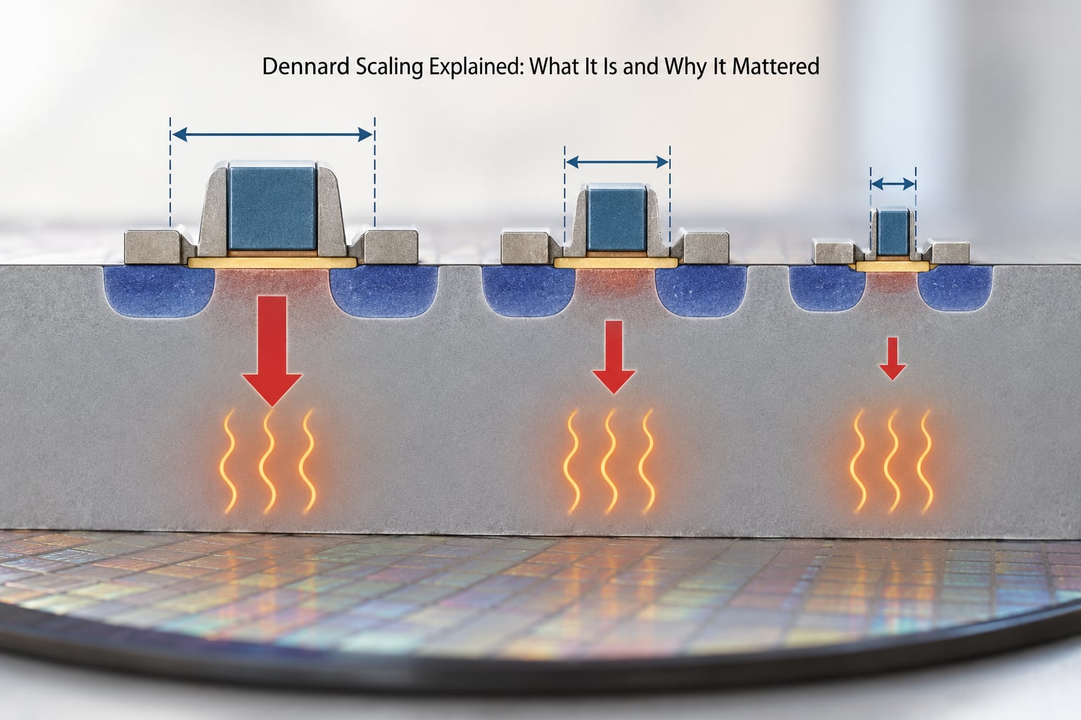
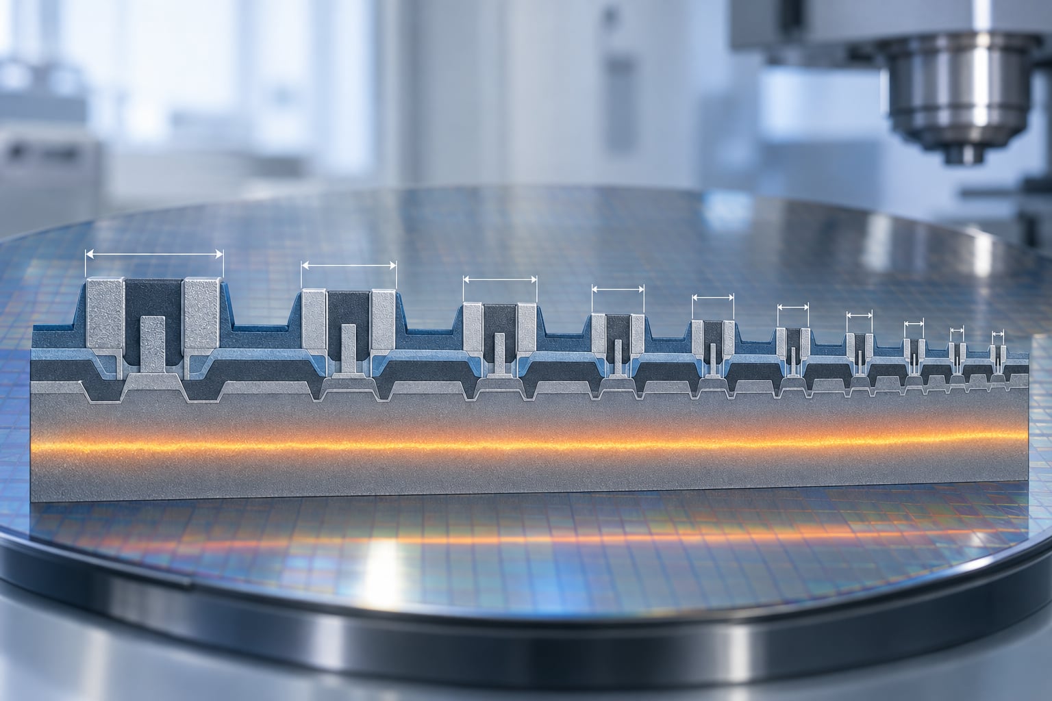
Robert H. Dennard and colleagues at IBM published the scaling law in the IEEE Journal of Solid-State Circuits in 1974. Their claim was that MOSFETs, the transistor type used in CMOS logic, could be scaled down uniformly in every dimension, with the voltage scaled by the same factor and the doping raised to compensate, and the result would keep power density constant.
Constant power density is the whole point. Power density is watts per square millimetre of silicon. If you halve every dimension of a transistor, its area drops by a factor of four, so you fit four times as many transistors per unit area. If each one uses a quarter of the power it did before, the silicon is working just as hard thermally as it was the generation before.
That is why the law mattered. Chip performance for most of the industry history came from raising clock frequency, and clock frequency costs power. With constant power density, a designer could add transistors, run them faster, and hand the package and heatsink roughly the same thermal load. Free performance, generation after generation.
What a transistor needs before scaling makes sense
A MOSFET has a gate, a source and a drain, and a channel of inversion charge connecting source and drain when the gate is above threshold voltage. In a CMOS circuit, transistors appear in pairs: an n-type pulling a node up, a p-type pulling it down, and both contributing switching energy every time the node flips.
The scaling rules only work if certain field ratios stay fixed. The vertical field across the gate oxide must stay roughly constant, or the oxide breaks down. The field between source and drain must stay roughly constant, or the channel stops behaving. The inversion layer thickness must shrink with the gate length, which is what keeps short-channel effects from taking over. Every rule below exists to protect one of those ratios.
How Does Dennard Scaling Change Transistor Performance?
Scaling a transistor by a factor K means dividing every dimension by K, dividing every voltage by K, and multiplying every doping concentration by K. Doing all three at once keeps the electric fields constant, keeps the gate overdrive voltage V_GT proportional to K, and keeps power density flat.
Dennard’s three scaling rules
1. Scale all dimensions by 1/K: gate length L, gate width W, gate oxide thickness t_ox, source and drain junction depth, and oxide and interconnect layer thicknesses.
2. Scale all voltages by 1/K: supply voltage V_DD, threshold voltage V_T, and every internal node swing.
3. Scale doping concentrations by K: source and drain doping, substrate doping N_A, and the implanted profiles, so that the junction depths shrink on the same schedule as the geometry.
The payoff falls out of the switching power relation P = C V² f. Capacitance C is roughly proportional to area times oxide thickness, so shrinking geometry by K divides C by K. Voltage drops by K, so V² drops by K². If the field ratios hold, the delay per stage drops by roughly K as well, which is why clock frequency could rise about 40 percent per generation while linear dimensions shrank about 30 percent.
Per transistor, power falls by K² (from voltage) and area falls by K² (from geometry). Those two K² reductions cancel, and that cancellation is the entire law.
A worked example: a 5 micrometre transistor scaled by K = 5
| Parameter | Before (5 micrometre device) | After K = 5 | What held constant |
|---|---|---|---|
| Gate length L | 5 micrometres | 1 micrometre | Source-drain electric field |
| Gate oxide thickness | 100 nm (1000 angstrom) | 20 nm (200 angstrom) | Oxide electric field |
| Source/drain junction depth | 0.5 micrometres | 0.1 micrometres | Doping-to-field ratio |
| Doping concentration | 0.5 x 10^16 per cm3 | 2.5 x 10^16 per cm3 | Inversion layer charge |
| Supply voltage V_DD | 5 V | 1 V | Gate oxide field, channel field |
| Threshold voltage V_T | 2 V | 0.4 V | Ratio V_GT / V_T |
| Transistors per unit area | 1x | 25x | Power density, watts per mm2 |
| Switching energy per transistor | 1x | 1/25x | Power density, watts per mm2 |
Read the last two rows together. Twenty-five transistors where there used to be one, each doing a twenty-fifth of the energy per switch, means the silicon is doing the same total work per square millimetre. That is the promise.
Now the assumption that never held. If you kept the geometry shrink but held the supply voltage at 5 V instead of dividing it by K, power per transistor would fall only by K (from the area-driven capacitance change), area would still fall by K², and power density would rise by K. At K = 5 that is a fivefold jump in watts per square millimetre. Nobody’s heatsink survives that.
Constant-field versus fixed-voltage scaling
| Parameter | Constant field (Dennard) | Fixed voltage | Plain meaning |
|---|---|---|---|
| Linear dimensions | 1/K | 1/K | Same shrink either way |
| Supply voltage V_DD | 1/K | 1 | Only Dennard lets voltage fall |
| Doping N_A | K | 1 | Doping rise holds the fields |
| Gate oxide electric field | 1 | K | Fixed voltage stresses the oxide K times harder |
| Drain current I_on | K | K | Current per device rises either way |
| Intrinsic delay t_pd | 1/K | 1/K | Speed gain comes from the shrink |
| Power density | 1 | K³ | The K³ is why fixed voltage is fatal |
| Delay x power product | 1/K² | K² | Constant field improves energy per switch |
Some treatments list the fixed-voltage power density exponent as K³ because capacitance per device falls by K while voltage is held, and the traditional derivation keeps the gate capacitance term separate. Either way the conclusion is identical and far more useful than the exponent: hold the voltage and the silicon runs out of thermal budget.
How Dennard Scaling Explained the Growth of Chip Density
Dennard scaling was the electrical half of density growth. The other half was lithography, and the two had to move together: every time photolithography printed a smaller gate, the process side had to deliver a thinner oxide, a shallower junction, a tighter overlay and a cleaner interconnect stack.
Process work did several things at once. Thinner gate oxides and higher-quality interfaces raised transconductance. Ion implantation, which Dennard’s original paper leaned on heavily, let dopant profiles be placed with atomic precision instead of relying on diffusion, which is what made controlled junction depths possible as the device shrank.
Interconnect got harder in parallel. Copper and low-k dielectrics replaced aluminium and silicon dioxide because wire resistance and RC delay were rising faster than transistor delay was falling. A transistor that is twice as fast behind a wire that is three times slower gains nothing, so interconnect scaling was never optional.
Put together with Moore’s law’s transistor-count doubling, the result was the pattern engineers saw for decades: roughly 30 percent smaller linear dimensions, roughly double the transistors, roughly 40 percent higher clock frequency, and roughly the same package power. Performance per joule doubled about every 18 months, which is the trend Jon Koomey later documented and named.
What Is the Difference Between Dennard Scaling and Moore’s Law?
Moore’s law said transistor counts on a chip would double on a regular schedule. Dennard scaling said that as transistors shrank, each one would use proportionally less power, so power per unit area would stay flat. Moore’s law counted things; Dennard scaling explained why making them smaller stayed affordable.
| Aspect | Dennard scaling | Moore’s law |
|---|---|---|
| What it describes | Power per unit area versus transistor size | Transistor count on a die over time |
| Type of statement | Physics of MOSFET design | Empirical observation about manufacturing |
| What it predicts | Constant power density, constant field ratios | Rapid and regular transistor-count growth |
| What it does not cover | How many transistors a designer chooses to build | Speed, power, cost per transistor |
| Status | Broke down around 2005 | Count still rising, cadence stretched to about two years |
Two misconceptions are worth clearing up here. First, constant power density never meant constant total power. Chip power did rise for decades, because transistor count rose faster than power per transistor fell once clock speed stopped absorbing the savings.
Second, smaller transistors did not automatically mean cheaper or better. A node name tells you very little about performance per watt; that depends on the transistor structure, the interconnect, the memory and the power management around it.
Why Did Dennard Scaling Eventually End?
Dennard scaling broke because two of its three rules stopped being physical. The doping rule hit a hard ceiling from atomic physics, and the voltage rule hit a hard ceiling from noise margin and heat. Sources disagree on whether to date the end to 2004, 2005, 2006 or 2007, and that disagreement is itself informative: each date marks a different company’s announcement, not a clean physical event.
Five reasons the law stopped holding
1. Quantum tunneling through the gate oxide. At a few nanometres the barrier is thin enough that electrons leak across it even when the transistor is off. Dennard’s own paper noted that sub-threshold behaviour does not scale with the rules.
2. The sub-threshold slope does not improve. Below threshold voltage, drain current falls with a slope set mostly by thermal physics, and that slope was roughly 60 mV per decade of current and stayed there. You cannot sharpen it by shrinking.
3. Leakage ate the power budget. With high enough off-state leakage across billions of transistors, static power climbed toward dynamic power, and dynamic power was the term the scaling rules were supposed to shrink.
4. The supply voltage hit a floor. Below roughly 0.7 V, signal-to-noise ratio, dynamic range and the voltage headroom needed to drive resistive wires stop improving. Since V² is in the power equation, V_DD stopped falling, and with it the constant-power-density result.
5. Interconnect and heat stopped scaling. Wire resistance per unit length, IR drop, RC delay and current density all worsened as wires got thinner, while electromigration reliability limits tightened. Heat removal also has a practical ceiling: the power density a package can shed caps clock frequency long before the silicon gives up.
That combination is why clock speeds plateaued in the 4 to 6 GHz range and why the Pentium 4’s high-frequency roadmap quietly became a dead end. The frequency plateau and the end of voltage scaling are two symptoms of one cause, and once you see them together the whole story is much easier to remember.
The design consequence is dark silicon. If transistor count doubles while the power budget stays fixed, each transistor only gets half the power, so a growing share of the die is powered off. Projections published around 2014 put the unusable fraction near a third of the die at 20 nm and up to roughly 80 percent by 5 nm. Those figures are old projections rather than measured results, but the direction held.
What Technologies Replaced Dennard Scaling?
The industry did not find a new single law. It stacked several partial answers, each recovering a slice of the performance that shrinking used to deliver for free.
- Multicore parallelism. Put more cores on the die and keep the per-core voltage and frequency flat. This works until software fails to parallelise, which is the practical version of Amdahl’s law.
- Specialised accelerators. GPUs, tensor accelerators, NPUs and DSPs trade generality for efficiency by running many narrow operations at low voltage, which is a deliberate move away from general-purpose scaling.
- High-k dielectrics and metal gates. A physically thicker oxide with a higher permittivity keeps the gate capacitance and the electric field under control when a plain silicon dioxide layer could no longer be made thin enough. This bought roughly a decade of planar scaling.
- FinFET and Gate-All-Around. Three-dimensional channel structures give the gate better electrostatic control over the channel, which fixes the short-channel behaviour that 2D transistors could not escape.
- Three-dimensional stacking and chiplets. Stacking cache and logic vertically, or splitting a large design into smaller dies joined by an advanced package, buys performance without pushing a single monolithic die past its power and yield limits.
- System-level efficiency. Power gating, voltage islands, non-volatile memory that can hold state without a refresh current, and smarter memory hierarchies all attack the cost of holding and moving bits.
How Does Dennard Scaling Relate to Modern Semiconductor Manufacturing?
Dennard scaling is still the mental model fabs and designers use, but the numbers behind a node name have stopped matching the name. A 5 nm label is not a 5 nm transistor. It is a marketing generation name, and the actual gate lengths and metal pitches depend on the specific process and the specific transistor structure.
The currency that replaced node naming is PPAC: performance, power and area, often normalised to a reference process. That framing exists precisely because the old single-number scale no longer describes what improves. A node can deliver better performance at similar area, better power at similar performance, or better density, and those three do not come together automatically.
Physical limits are now shared between the transistor and everything around it. Design-technology co-optimisation means the standard cell library, the SRAM bitcell, the interconnect stack and the power-delivery network are designed together rather than sequentially. Leakage, IR drop and electromigration are checked against the same budgets as logic density, and on an advanced node those interconnect and power-delivery constraints bind before the transistor does.
For anyone reading a roadmap, the useful habit is to ask which quantity is being optimised and at what power budget. Density alone stopped being free a long time ago.
Frequently Asked Questions
What does Dennard scaling mean?
Dennard scaling, also called MOSFET scaling, is a 1974 law stating that if you divide all transistor dimensions by a factor K, divide all voltages by K, and raise doping by K, the electric fields stay constant and power per unit area stays constant. You can then fit K times more transistors per unit area with the same thermal load.
Why was Dennard scaling important for CPUs?
It removed the thermal cost of progress. With power density constant, engineers could shrink devices, raise clock frequency about 40 percent per generation, and add transistors without a bigger heatsink. That is where decades of steady single-core speed gains came from, until voltage scaling stopped around 2005.
Is Dennard scaling the same as Moore’s law?
No. Moore’s law is an observation that transistor counts rise on a regular schedule. Dennard scaling is a physics statement about power per unit area when transistors shrink. Moore’s law counted the transistors; Dennard scaling explained why making them smaller stayed affordable. One has slowed in cadence, the other has stopped working.
When did Dennard scaling stop working effectively?
Sources cite 2004, 2005, 2006 or 2007 because each marks a different company’s announcement rather than a single physical moment. The practical break was around the 90 nm generation, when quantum tunneling leakage, a sub-threshold slope that would not improve, and a supply voltage floor near 0.7 V together ended the constant-power-density result.
What replaced Dennard scaling in modern chips?
A stack of partial answers: multicore parallelism, specialised accelerators such as GPUs and NPUs, high-k dielectrics with metal gates, FinFET and Gate-All-Around transistor structures, 3D stacking and chiplets, plus power gating and non-volatile memory. Together they recover performance without shrinking voltage and power density at the old rate.
Does a smaller process node automatically mean better performance?
No. Node names are marketing labels rather than exact feature sizes, and a smaller number does not guarantee better performance per watt. Evaluate performance, power and area together, because a process can improve one at the cost of another, and interconnect plus power delivery often bind before the transistor itself does.
Conclusion: Start With the Scaling Principle
If you take one idea away, make it this: smaller dimensions only turned into higher density when voltage, power and physical limits were managed together. Dennard scaling described the combination that worked for thirty years, and its failure tells you why clock speeds plateaued and why multicore, accelerators and 3D packaging exist today.
Start with the constant-field assumption. Everything else follows from it.