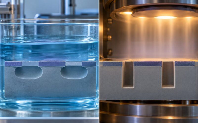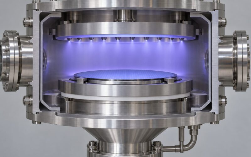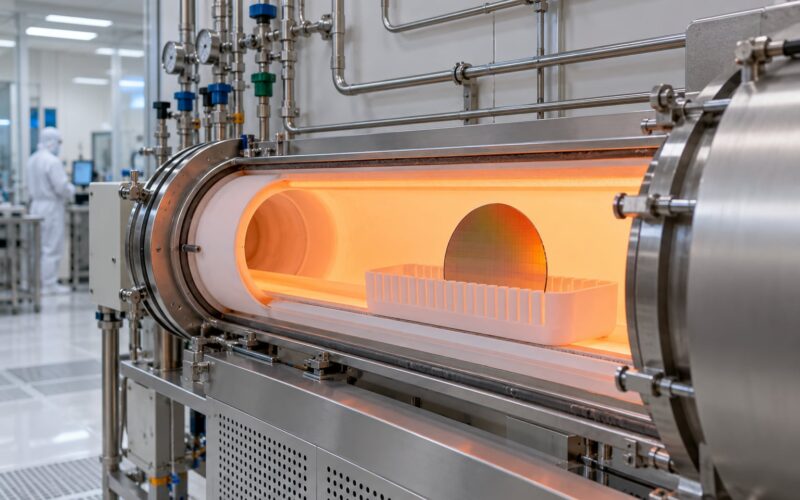
Think of chip making as repeated printing. A machine shines light through a stencil onto a light-sensitive coating on a silicon wafer, and where the light lands, the coating changes so a later chemical step can etch or fill that spot. Everything a chip can do comes down to how small and how accurate those printed shapes are.
Immersion lithography explained in one sentence: it is optical patterning in which a high-refractive-index liquid, almost always ultrapure water, fills the gap between the projection lens and the wafer so the system can print smaller features from the same 193nm light. That one change broke the resolution limit that had stalled optical patterning, and it is why leading-edge logic and most memory layers got made at all. Updated for 2026.
The rest of this article works through the mechanism, the process, and the four engineering problems that decide whether the extra resolution is worth anything on a real production line.
Table of Contents
- What Is Immersion Lithography?
- How Does Immersion Lithography Work?
- Why Does Immersion Lithography Improve Resolution?
- How does the k1 factor limit what immersion can print?
- What Is the Difference Between Dry and Immersion Lithography?
- What Liquid Is Used in Immersion Lithography?
- What Are the Main Advantages and Challenges?
- How Do Semiconductor Fabs Control Immersion Lithography Defects?
- How Does Immersion Lithography Fit into Advanced Chip Manufacturing?
- Frequently Asked Questions
- Can you explain lithography in a simple way?
- What is immersion lithography?
- How does immersion lithography increase resolution?
- What is the difference between immersion and dry lithography?
- What problems does immersion lithography cause?
- Does EUV lithography make immersion lithography obsolete?
- Conclusion
What Is Immersion Lithography?
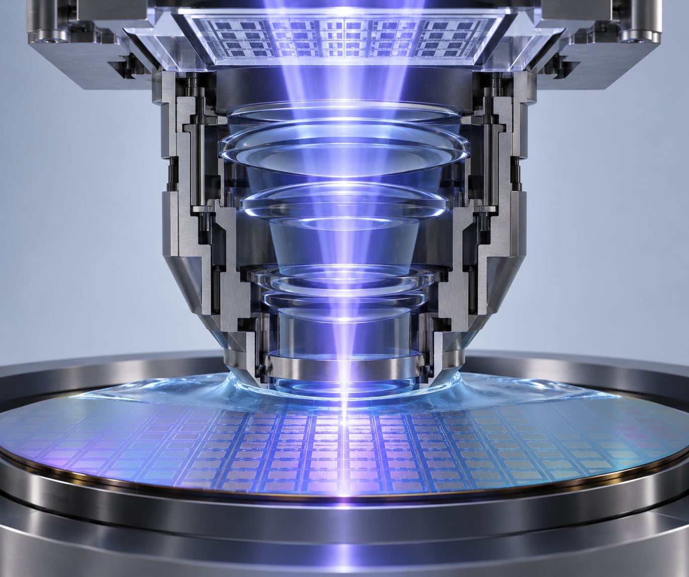
Immersion lithography is a semiconductor patterning technique that puts a liquid between the last element of a projection lens and the wafer surface, raising the optical system’s numerical aperture so smaller features can be printed without changing the light source.
Conventional, or dry, projection lithography works with an air gap between the final lens element and the resist-coated wafer. Immersion replaces that air with water, which bends light more strongly than air does and lets the lens collect a wider cone of light onto the wafer. Higher numerical aperture means a smaller printable feature for the same wavelength.
In practice, immersion lithography is not a niche variant. It is the technique behind 193nm ArF immersion, usually abbreviated ArFi, which carried patterning from roughly the 65nm generation down through 32nm, 22nm, 14nm and into 7nm-class logic, plus the dense metal and via layers of DRAM and NAND flash. The lithography scanners built for it are also the workhorse tools in almost every front-end fab running deep ultraviolet, or DUV, processes.
Two things immersion does not do are worth stating up front. It does not remove the need for multi-patterning once feature pitches get tight enough, and it does not shrink the pitch limits set by the resist chemistry or by how well the pattern can be etched and measured. It buys resolution inside a fixed wavelength, which is a large gain and still not an infinite one.
How Does Immersion Lithography Work?
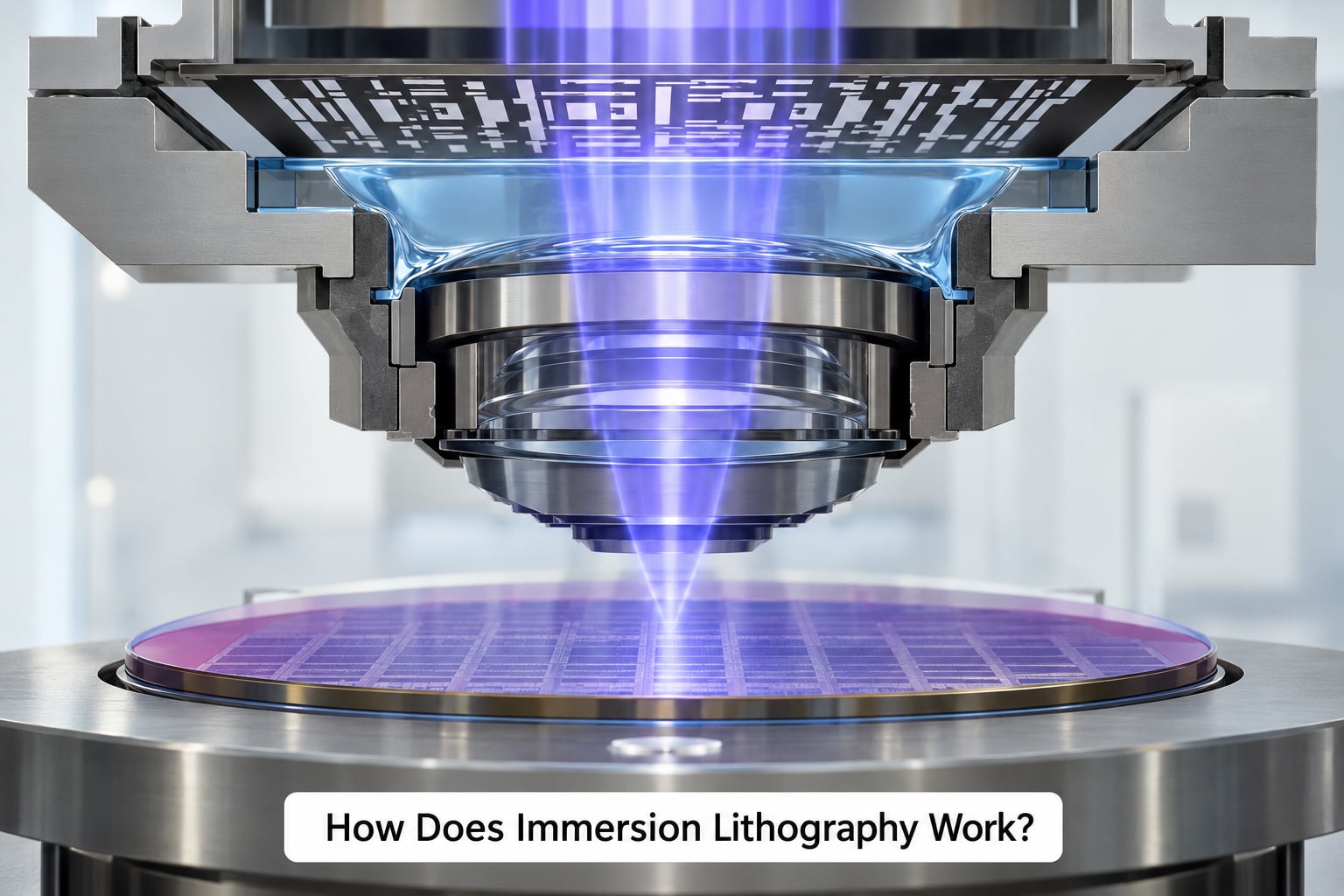
A single exposure in an ArF immersion scanner runs in a fixed order. Understanding the sequence matters, because almost every immersion defect traces back to one of these steps.
- Coat the wafer. A spin coater lays down a photoresist film, roughly a few hundred nanometres thick, and bakes off the solvent. Modern production resists often carry a separate hydrophobic topcoat above the imaging layer.
- Align. The wafer stage moves under the optics until the scanner’s alignment sensors match the wafer to previously printed layers. Any error here becomes overlay error on the finished device.
- Fill the gap with water. The immersion head lowers and traps a thin film of ultrapure water between the final lens element and the resist. Small nozzles supply and recover liquid continuously; an air curtain keeps droplets off the lens above.
- Project the mask pattern. A 193nm argon fluoride excimer laser feeds the projection optics, which reduce the reticle pattern by a factor of four and focus it through the water onto the resist.
- Scan the field. The wafer stage sweeps under the lens at high speed so the whole reticle field is exposed, then steps to the next field. In line-and-space patterning the scan direction is orthogonal to the pattern orientation, which keeps leading and trailing edges clean.
- Drain and develop. The head drains the water, the wafer gets a post-exposure bake, and a developer dissolves the exposed resist, leaving the pattern standing on the surface.
- Harden and transfer. A hard bake fixes the image, and the pattern is moved into the layer below by an etch or used as a mask for a deposition step.
- Measure. A scanner checks the pattern against the design rules that the mask maker encoded in the reticle, flagging bad fields before the wafer leaves the tool.
Nikon shipped the NSR-S609B as the first production ArF immersion scanner, and the basic sequence above has stayed recognizable across every generation since. What changed is throughput, overlay performance, and how tightly the head controls the liquid.
Why Does Immersion Lithography Improve Resolution?
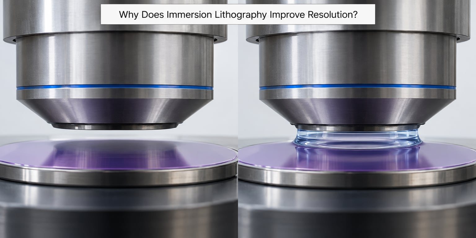
Resolution improves because the wavelength of light inside the medium is shorter and because the lens can gather a wider cone. Two numbers explain both effects: refractive index and numerical aperture.
Refractive index, usually written n, says how much light slows down in a material. Air is about 1.0. Water at the 193nm imaging wavelength is about 1.44. When light crosses from a lens into water, its wavelength shrinks by that ratio, so a 193nm beam behaves as though it were closer to 134nm inside the gap. Shorter effective wavelength means the lens can separate features that are closer together.
Numerical aperture, or NA, measures how wide a cone of light the lens collects. Bigger cone, smaller spot. Dry ArF tools top out around NA 0.93. Immersion tools reach NA 1.35, and that is the number the industry quotes when it describes the gain.
The classic resolution relationship is the Rayleigh formula:
R = k1 × λ / NA
R is the resolvable feature size, λ is the wavelength, NA is the numerical aperture, and k1 is a lumped process factor that captures everything optical and chemical the equation cannot name. Smaller R is better, so you raise NA or shrink the effective wavelength.
Worked example at 193nm with k1 = 0.25. Dry at NA 0.93 gives R = 0.25 × 193 / 0.93, which is about 52nm. Immersion at NA 1.35 gives R = 0.25 × 193 / 1.35, which is about 36nm. Same laser, same wavelength, same resist, roughly a 30% smaller printable feature. That single comparison is why immersion beat dry ArF so decisively.
How does the k1 factor limit what immersion can print?
The k1 factor is where lithography runs out of road. It has fallen from around 0.5 in the 1980s to about 0.25 today, and every step down since then has cost real effort: reticle and mask corrections, source shaping, off-axis illumination, resist chemistry tuned to the point where it almost seems to break. Below roughly k1 = 0.25 the approach stops scaling cleanly, and further progress has to come from NA or from patterning with the same feature more than once.
That is the cliff concept in one line. Immersion pushed NA high enough to keep k1 in a workable range for the 2010s. It could not push it much past 1.35, which is why multi-patterning and then EUV arrived.
What Is the Difference Between Dry and Immersion Lithography?
The two differ mainly in what sits in the lens-to-wafer gap, and that one difference cascades into resolution, defect behaviour, and process complexity.
| Factor | Dry 193nm ArF | Immersion 193nm ArF (ArFi) |
|---|---|---|
| Medium in the lens gap | Air | Ultrapure water |
| Typical NA | Up to about 0.93 | Up to 1.35 |
| Resolvable feature, k1 = 0.25 | About 52nm | About 36nm |
| Depth of focus | Moderate | Longer relative to the feature size |
| Dominant defect risk | Particles, focus and overlay | Plus bubbles, water marks, leaching, thermal drift |
| Wafer throughput | Generally lower | Roughly 148 to 250+ wafers per hour on current platforms |
| Process complexity | Straightforward resist and coat-develop flow | Adds liquid supply, recovery, thermal control and extra monitoring |
| Typical role in the fab | Non-critical and older layers | Critical layers from about the 65nm node onward, plus dense interconnect |
Dry ArF has not disappeared. Many mature-node fabs run it for layers that do not need the resolution, because a tool that never touches water is a tool with a smaller defect list. Immersion earns its extra complexity wherever feature size actually matters.
What Liquid Is Used in Immersion Lithography?
The immersion liquid is ultrapure water, deionised and filtered to semiconductor grade. Alternative liquids such as perfluorinated compounds were investigated, but none matched water’s combination of optical, physical and chemical properties at a practical cost.
Water wins on four counts. Its refractive index near the imaging wavelength is high enough to deliver the resolution gain. It flows and drains cleanly at thin film thicknesses. It is chemically compatible with the lens coatings and the resist stack, and it dissipates the heat that a high-power laser dumps into the gap. It is also simply available in enormous quantities at a grade that a fab already knows how to deliver.
The costs of using water are real. Its index changes with temperature at roughly minus one ten-thousandth per kelvin, which is why liquid stability on the order of ten millikelvin matters for imaging stability. It can leach components out of the topcoat if the chemistry is not balanced, and it leaves mineral residue if it evaporates in the wrong place. Water is not an inert convenience; it is a chemical participant that has to be controlled like one.
What Are the Main Advantages and Challenges?
The advantages are mostly optical, but the ones that mattered commercially are process-side.
- Finer features at the same wavelength. Roughly 30% smaller resolvable feature than dry ArF at equal k1.
- More depth of focus per feature size. Wider focus margins make step heights and wafer topography less punishing.
- Compatibility with existing infrastructure. Same 193nm laser, same reticle infrastructure, same resist platform as dry ArF. Fabs could adopt it without replacing the whole tool ecosystem.
- High throughput. Production ArFi platforms reach hundreds of wafers per hour, which is what makes single exposure economically preferable to patterning something three times.
The challenges are concentrated in liquid handling and in anything that puts a physical object between the lens and the wafer.
- Bubbles. An attached bubble large enough to scatter light prints a defect directly into the resist. Industry work suggests attached bubbles above roughly 60nm can do damage, while freely floating bubbles are largely harmless at production ratios.
- Particles and contamination. Anything in the water or on the wafer lands in the image. Water purity and wafer surface preparation are continuous concerns, not one-time checks.
- Water marks and droplet residue. Draining leaves a receding meniscus at the wafer edge. If it retreats far enough it can tear and leave a residue ring.
- Thermal effects. Laser energy heats the liquid, the heated liquid changes refractive index, and the focus shifts. Millikelvin-level stability is the design target.
- Lens stress and contamination. Pressurised water acting on glass elements can distort them and introduce birefringence, and a single speck on the final element sits in every exposure.
- Yield risk from complexity. More moving parts and more fluid paths mean more ways to lose a wafer.
How Do Semiconductor Fabs Control Immersion Lithography Defects?
Fabs manage immersion defects through a combination of hardware design, chemistry, and process recipes rather than any single fix.
- Water purity and filtration. Supply water is filtered to sub-micron and in some cases trace-particle levels below what the imaging wave can resolve, and the loop is continuously monitored so a spike is caught before wafers are affected.
- Wafer and lens surface preparation. Hydrophobic topcoats and surface treatment keep water from beading. Scanners include wafer-contact cleaning and lens-element cleaning steps that run between exposures or fields.
- Bubble prevention. Dissolved gas is managed in the loop, and nozzle geometry and flow rate are tuned so the water film forms without entraining air. Faster scanning makes this harder, which is why throughput work and defect work are the same project.
- Meniscus and contact angle control. The aim is a receding contact angle that stays far enough from zero that the meniscus never tears. Vendor and academic work on critical velocity treats this as the parameter that limits how fast a wafer can scan.
- Temperature stability. The liquid is held to a tight tolerance, and the optics themselves are temperature-controlled to remove focus drift from the equation.
- Drain and recovery. After exposure the water is pulled off in a controlled way, and the wafer is dried before it leaves the tool, because evaporated residue is permanent on the resist.
- Metrology and recipes. In-line defect inspection, overlay monitors, and per-product recipes that tune focus, dose, and scan speed turn a fragile step into a repeatable one.
The practical lesson is that immersion defect control is mostly about velocity. Anything that raises the speed at which the wafer moves through the water raises the stress on the meniscus, and that is why a throughput increase and a defect reduction are usually the same engineering problem.
How Does Immersion Lithography Fit into Advanced Chip Manufacturing?
Immersion lithography is one step in a long patterning loop, and it only makes sense alongside the rest of it. Resist chemistry determines what the optics can resolve and how the image survives etching. Mask design, with optical proximity correction and source mask optimization, moves the process closer to what the optics can actually print. Etch and deposition steps transfer the printed pattern into conductors and insulators. Metrology and overlay monitoring catch the fields that drifted.
Where immersion stops, multi-patterning starts. Practitioners commonly put the practical back-end-of-line pitch limit for single ArFi exposure around 80nm, with self-aligned double patterning carrying roughly to a 40nm half-pitch and quadruple patterning needed below that. Scotten Jones of SemiWiki has argued those figures in forum discussions, and they are a useful working estimate rather than a physical law. The cost is real: more masks, more exposures, tighter overlay budgets between passes, and yield loss from the compounding error. That complexity, more than the exposure tool itself, is what makes multi-patterning expensive.
This also explains why node names mislead. A product’s stated node says little about the pitch that was actually printed, so you cannot infer which patterning technique was used from the name on the box.
EUV at 13.5nm changes the picture by replacing the need for multiple exposures at the most critical layers, using reflective multi-layer optics in a vacuum. High-NA EUV pushes toward NA 0.55 to print smaller features in one pass. Immersion is not obsolete in 2026. It still patterns the majority of layers on any advanced chip, including most of the interconnect stack, and EUV tools remain far more expensive and lower in throughput than mature ArFi platforms.
One footnote on supply: EUV scanners are made by a single supplier, ASML, and the reason is that a working EUV source at production power, plus the optics and masks to go with it, took more than a decade of concentrated industrial effort. That is a business fact about the supply chain, not a physics limit on immersion.
Frequently Asked Questions
Can you explain lithography in a simple way?
Chip making repeats one basic move many times. A stencil called a reticle sits above a silicon wafer coated in a light-sensitive chemical, and a machine projects light through the stencil onto that coating. Light changes the coating so a later bath dissolves it away, leaving a tiny pattern. Etching or filling copies that pattern into the layers below, and stacking the layers builds a transistor. Lithography is the printing step that defines where every feature goes.
What is immersion lithography?
Immersion lithography is optical patterning in which a high-refractive-index liquid, almost always ultrapure water, fills the gap between the projection lens and the wafer. Because water bends light more than air does, the lens can collect a wider cone of light, raising numerical aperture and letting the same 193nm source print smaller features. It is the basis of ArF immersion, or ArFi.
How does immersion lithography increase resolution?
Water has a refractive index near 1.44 at the imaging wavelength, about 1.0 for air, so light travelling through the gap behaves as though its wavelength were roughly a third shorter. At the same time the higher refractive index allows a much wider collection cone, taking numerical aperture from about 0.93 in dry ArF to 1.35. Using R = k1 x wavelength / NA, both effects together shrink the printable feature by around 30 percent.
What is the difference between immersion and dry lithography?
Dry lithography leaves an air gap between the lens and the wafer and is limited to a numerical aperture near 0.93. Immersion fills that gap with ultrapure water and reaches NA 1.35, printing smaller features from the same laser. The trade is complexity: immersion adds liquid supply and recovery, bubble and meniscus control, thermal stability requirements and extra monitoring, which is why mature layers often still use dry ArF.
What problems does immersion lithography cause?
The main problems are bubbles, particle contamination, water marks from a receding meniscus, thermal drift of the liquid, and lens contamination and stress. Bubbles large enough to scatter light print defects straight into the resist, and evaporation in the wrong place leaves permanent residue. Because of these, immersion adds moving fluid paths to a process that was previously mechanically simple, and throughput increases make meniscus control harder rather than easier.
Does EUV lithography make immersion lithography obsolete?
No. EUV at 13.5nm removes the need for multiple exposures at the most critical layers, and high-NA EUV promises smaller single-exposure features. Even so, ArF immersion still patterns the majority of layers on an advanced chip, most of the interconnect stack included, and EUV tools cost far more and run at lower throughput. Analysts generally treat the two as overlapping for years rather than as a clean handover.
Conclusion
Immersion lithography improved resolution by filling the lens-to-wafer gap with a high-index liquid, which raised numerical aperture from about 0.93 to 1.35 and shrank the printable feature by roughly a third without changing the 193nm light source.
If you take one idea from this article, make it the trade. That resolution gain is optical and clean, but every gain came with liquid-handling problems: bubbles, meniscus stability, thermal drift, residue and lens contamination. Start with why water changes the effective wavelength and the collection cone, then read the defect controls as the price of that gain.