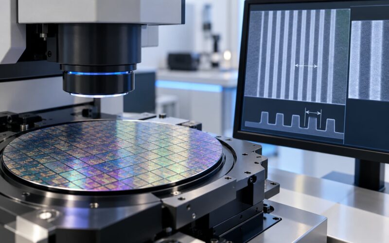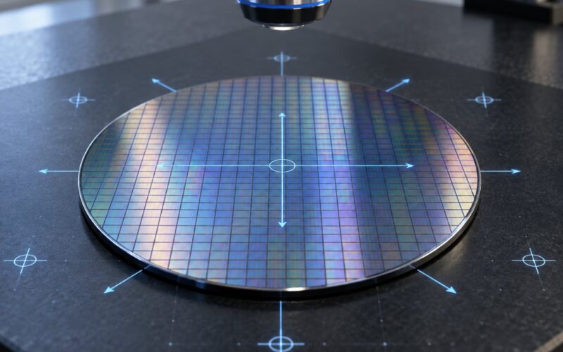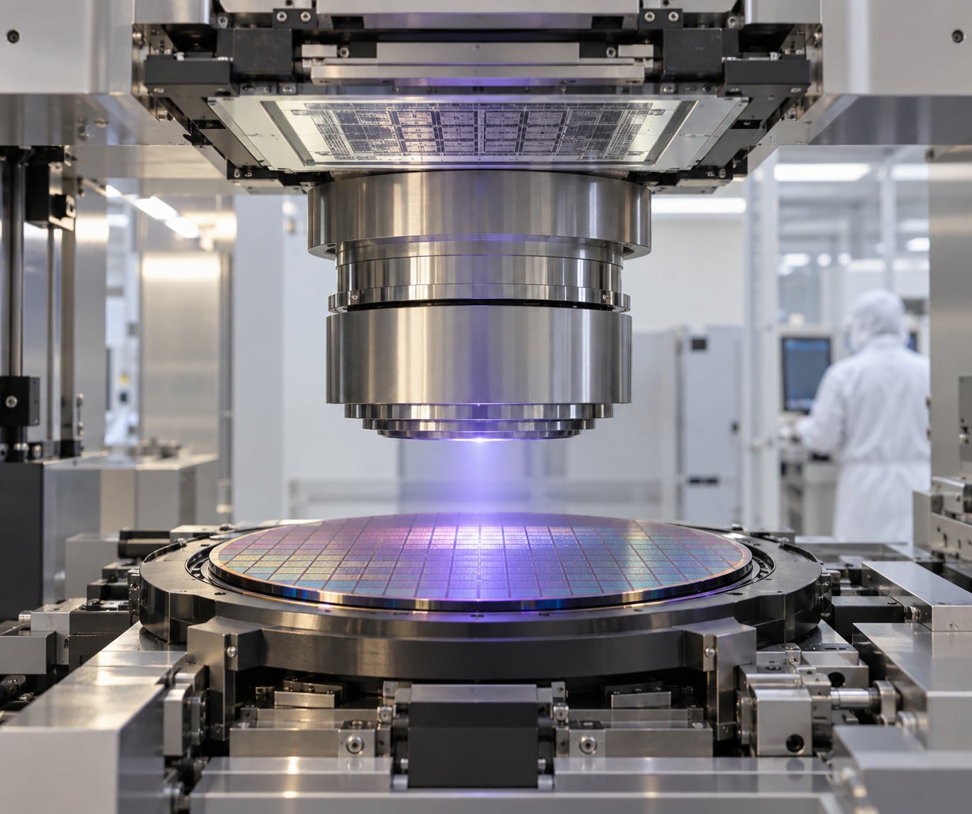
A reticle is the patterned glass plate that holds a chip’s circuit layout, and a stepper is the machine that repeatedly prints that layout onto a light-sensitive coating on a silicon wafer. Those two facts cover most of reticle and stepper basics, but the useful part is what happens between them: light passes through or reflects off the mask, reduction optics shrink the pattern onto photoresist, and the stage moves the wafer so the same die gets printed over and over until the whole wafer is covered.
If you are new to semiconductor manufacturing, that one paragraph is enough to follow a fab process flow. The rest of this guide fills in the details that trip people up, including why a mask pattern is drawn several times larger than the final feature, how alignment decides whether layer two lands on top of layer one, and which defects come from the reticle versus the process.
Table of Contents
- What Is a Reticle in Semiconductor Manufacturing?
- Reticle size and the scaling convention
- Is a reticle the same thing as a mask?
- What is on the plate besides the pattern?
- Clear-field and dark-field layouts
- What Does a Lithography Stepper Do?
- Reticle and Stepper Basics: How One Print Cycle Works
- Reticle and Stepper Terms at a Glance
- How Do Reticles and Steppers Create Tiny Circuit Features?
- Why the node name is not a capability
- How the mask is corrected for the optics
- How Are Wafers Aligned Before Exposure?
- What Defects Can Appear in a Reticle Image?
- Mask-related defects
- Process-related defects
- What Is the Difference Between a Reticle and a Stepper?
- Where Do Reticles and Steppers Fit in the Chipmaking Process?
- Who makes the tools?
- A note on DIY lithography
- Frequently Asked Questions
- Is a reticle the same as a photomask?
- What does a lithography stepper print, and how often does it repeat?
- How do stepper resolution and numerical aperture differ?
- Why does overlay matter even when a layer looks correctly exposed?
- Can a reticle defect be corrected without replacing the mask?
- How do EUV steppers differ from traditional DUV steppers?
- Conclusion: Start with the Exposure Workflow
What Is a Reticle in Semiconductor Manufacturing?
A reticle in semiconductor manufacturing is a transparent plate, usually fused quartz, coated with a patterned absorber layer that encodes the layout for one layer of a chip. The clear areas pass light, the dark areas block it, and that contrast is what the stepper projects onto the wafer.
The absorber used to be a chrome-like metal, and you will still hear people call it the chrome layer. More advanced masks use other materials, including molybdenum silicide for EUV work and phase-shifting films that do not simply block light but change its phase. More on those later.
Reticle size and the scaling convention
Here is the part that surprises most newcomers. The pattern on a reticle is not drawn at final size. It is drawn larger than the wafer geometry, typically four or five times larger, and the projection optics demagnify it during exposure. The usual industry range is 2x to 10x, with 5x the most common convention.
Printing larger and shrinking optically exists for a practical reason. A feature printed at one-fifth scale is one-fifth the size on the reticle, so a mask defect or particle has to be tiny to matter. It also gives the mask maker room to place many copies of one die in a single exposure field, which is how a stepper covers a whole wafer without reloading a mask for each chip.
Is a reticle the same thing as a mask?
Yes. Reticle, photomask, and mask are used interchangeably for the same patterned plate in most fabs. The one distinction people draw is by scale: a mask usually means the pattern is written 1:1, while a reticle usually means the pattern is written larger than final size and reduced optically. A 5x reticle is a mask in the everyday sense and a reticle in the fab sense, and nobody is wrong for calling it either.
What is on the plate besides the pattern?
A thin transparent membrane called a pellicle sits a few millimetres above the pattern. Particles that land on the pattern would otherwise print as missing features, because the stepper’s depth of focus blurs them out at the wafer while leaving the pattern sharp. A pellicle catches the particle in mid-air, where it never reaches the mask surface.
Clear-field and dark-field layouts
Which parts of the mask carry absorber matters more than beginners expect. In a dark-field layout, the absorber sits where the features go, and light floods the gaps. In a clear-field layout the arrangement flips, so open areas are bright and the pattern sits in shadow. Clear-field masks scatter less stray light back into the optics, but any particle on them lands somewhere that gets printed instead of being masked by an opaque region.
What Does a Lithography Stepper Do?
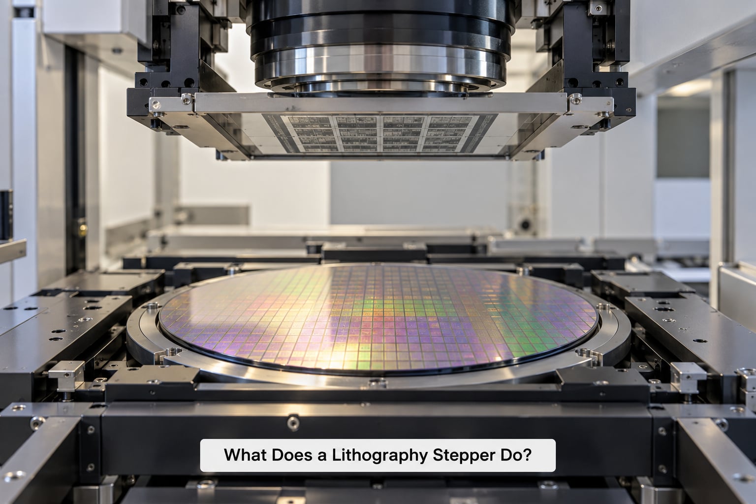
A lithography stepper does four things in a loop: it holds the reticle above the wafer, floods the reticle with light, projects a reduced image of the pattern onto photoresist through a set of projection lenses, and then moves the wafer stage sideways to the next die and repeats. The name comes from that stepping motion, step-and-repeat being the older term for exactly this cycle.
Inside the tool you will find a light source, a condenser and projection lens stack, a reticle stage that holds and moves the mask, a wafer stage with nanometre-level positioning, an alignment system, and a focus and dose control loop. Steppers print one die at a time and move. Scanners, by contrast, expose a narrow slit while the reticle and wafer move together, which allows a much larger field and better resolution at the cost of far more complex mechanics.
Reticle and Stepper Basics: How One Print Cycle Works
Every print cycle follows the same order, whether the tool is a simple mask aligner or a full production stepper.
- Load and level the wafer. The robot places the wafer on the stage, a notch or flat identifies its orientation, and the stage tips until the surface sits flat enough to expose. Stage flatness errors translate directly into focus errors.
- Find the alignment marks. Sensors read the marks etched into a previous layer, often with a dedicated alignment wavelength that does not expose the resist.
- Compute the correction. The tool works out the small x, y, and rotation offsets needed to land this layer on the last one, then stores them as a wafer map.
- Set focus and dose. A focus sensor measures the gap to the resist and the illumination is trimmed until the delivered energy matches the target dose for the chemistry in use.
- Place the reticle. The reticle stage moves the mask into the optical path and holds it for the exposure.
- Expose one die. Light passes through the clear mask regions, the projection optics demagnify the image, and the resist records the pattern.
- Step to the next die. The wafer stage advances by exactly one die pitch, including the small inter-die gap, and the cycle repeats.
- Develop after the last field. Once a whole wafer is exposed, it goes to a track where the soft bake, post-exposure bake, and develop chemistry turn the exposed resist into a physical pattern that protects the layer underneath.
Steps two and three are what people mean when they ask how layers stack up. Everything else is how a single layer gets printed correctly on its own.
Reticle and Stepper Terms at a Glance
These nine terms carry most of the vocabulary you will meet in fab conversations and documentation.
| Term | What it means |
|---|---|
| Reticle (photomask) | The patterned quartz plate holding the layout for one layer, drawn larger than final size. |
| Stepper | The exposure tool that aligns the reticle, prints one die, moves, and repeats across the wafer. |
| Photoresist | The light-sensitive polymer coating on the wafer that records the pattern and later protects it. |
| Exposure field | The rectangular area the optics can print in one shot, containing one or more die. |
| Die | A single copy of the circuit layout, repeated across the wafer. |
| Alignment mark | A reference feature on the wafer that the tool measures to position each layer. |
| Numerical aperture (NA) | A measure of how wide a cone of light the lens collects, written as NA and driving resolution. |
| Resolution | The smallest feature the process can print reliably at a given wavelength and NA. |
| Overlay | How closely a new layer lines up with the layers already on the wafer. |
How Do Reticles and Steppers Create Tiny Circuit Features?
Two levers set the size limit: the wavelength of the light and the numerical aperture of the projection lens. The Rayleigh criterion puts them together as R = k1 × λ / NA, where R is the resolvable feature, λ is the exposure wavelength, NA is the numerical aperture, and k1 is a factor that captures how much the process and the mask engineering improve on the raw optical limit.
Here is a worked example with an argon fluoride immersion tool. At a wavelength of 193 nm and an NA of 1.35, a k1 value of 0.25 gives R = 0.25 × 193 / 1.35, which is roughly 36 nm of half-pitch capability. Push k1 down to 0.20 with better optics and computational correction and the same tool reaches about 29 nm. Now switch to EUV at 13.5 nm with an NA around 0.33 and a comparable k1, and the formula lands near 10 nm.
That single equation explains most of the last decade of the industry. ArF dry printing stalled around the 65 to 45 nm era because the wavelength was fixed and only k1 was left to squeeze. Immersion lithography, which puts a liquid of higher refractive index between the lens and the wafer, raises the effective NA and buys back most of that gap. EUV changes the wavelength itself and took resolution down another threefold.
Why the node name is not a capability
A node label such as 7 nm or 3 nm is a marketing name inherited from gate length scaling, and it has never matched the smallest printed dimension. Compare two processes labelled with the same node and you can find meaningful differences in minimum metal pitch, density, and design rules. When you evaluate a lithography platform, look at resolution, overlay, field size, and throughput instead.
How the mask is corrected for the optics
Because real optics do not print what a layout draws, masks are pre-compensated. Optical proximity correction reshapes corners and extends line ends, since a lone line end diffracts differently from a line in a dense array. Phase-shifting masks go further by making adjacent regions shift the light’s phase by 180 degrees, so dark areas form through interference rather than simple blockage. That idea came from fundamental wave optics long before EUV existed, and it is still in use in modified form.
How Are Wafers Aligned Before Exposure?
Alignment starts with reference marks. A dedicated set of marks is laid down on the wafer during an early layer, and every later layer measures those same marks to know where it currently sits relative to the design. Stepper tools typically use one mark set for coarse placement and another for fine, high-accuracy correction, because grabbing a mark from a global position takes a while and grabbing a nearby one is quick.
Here is the sequence. The wafer stage scans the coarse marks and computes a rotation angle and translation for the whole wafer. It then moves to a local site and reads the fine marks with a dedicated sensor. Any residual offset from last layer, thermal drift, and stage error is folded into a correction stored per die or per wafer. Before each exposure, the correction is applied to the stage so the new field lands where the process window expects it.
Overlay is usually quoted as a small number in nanometres, and it is measured after the resist is developed and the pattern is etched. Good overlay means layer two registers to layer one closely enough that vias connect, contacts land inside diffusions, and interconnect lines do not wander into their neighbours. Poor overlay does not necessarily mean the exposure was wrong; it usually points at stage metrology, thermal control, or a wafer that moved after alignment.
What Defects Can Appear in a Reticle Image?
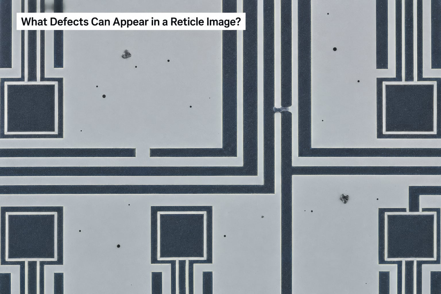
Defects fall into two groups: things wrong on the mask, and things wrong in the process. Telling them apart quickly saves a lot of wasted investigation.
Mask-related defects
- Missing features. An absorber patch that should be opaque is partly or entirely transparent, printing a feature that was never on the layout.
- Bridges. Absorber that extends past one feature and touches a neighbour, merging two lines into one.
- Pinholes. Tiny transparent holes in an opaque region, printing bright spots in what should be dark.
- Scratches and absorber defects. Damage from handling, writing, or cleaning that distorts the pattern locally.
- Particles on the mask. Usually handled by the pellicle, but a particle that escapes still prints as a defect at the mask position.
- Placement error. The pattern sits off its intended position on the reticle, which becomes a systematic offset across every die printed from that field.
Process-related defects
- Focus error. The resist sits outside the depth of focus, and lines blur at their edges.
- Dose error. Underexposure leaves resist behind, overexposure thickens features and can close a nominal gap.
- Developer and track issues. Standing waves, residue, and non-uniform development change critical dimensions after a perfectly good exposure.
- Etch and deposition artefacts. Loading effects, undercut, and via slumping all show up on the wafer without any lithography fault at all.
Because a reticle prints many dies, a single mask defect can appear on hundreds of chips. Mask makers deal with this through inspection tools that compare a mask against its source data at multiple wavelengths, aerial imaging systems that check what the mask actually projects, and repair systems that deposit or remove absorber at flagged sites. EUV masks complicate all of this because they are reflective rather than transmissive, and a pellicle for them must pass extreme ultraviolet wavelengths.
What Is the Difference Between a Reticle and a Stepper?
The reticle stores the pattern; the stepper positions and exposes it. One is a consumable precision plate produced per chip layer, the other is a multi-hundred-million-dollar machine reused for every layer in the fab. Everything else follows from that split.
| Aspect | Reticle (photomask) | Stepper |
|---|---|---|
| Role | Holds the circuit layout for one layer | Prints that layout onto the wafer, repeatedly |
| Lifespan | Made per mask set, replaced or repaired as needed | Capital equipment used for the life of the fab |
| Pattern type | Binary, attenuated phase shift, alternating phase shift, reflective for EUV | DUV stepper, DUV scanner, or EUV scanner |
| Resolution role | Corrected pattern written at 4x or 5x, sets what the optics can resolve | Wavelength, NA, and k1 set the printed feature size |
| Defect sensitivity | One defect repeats across every die in the field | Focus, dose, and placement errors vary per field |
| Key specification | Critical dimension uniformity and placement accuracy on the mask | Resolution, overlay, field size, and throughput |
One point of confusion is worth naming outright. People often say stepper as a generic term for any lithography tool. That is technically wrong but widely understood, and most leading-edge production exposure today happens on scanners, which use step-and-scan motion rather than step-and-repeat.
Where Do Reticles and Steppers Fit in the Chipmaking Process?
Lithography sits in front-end fabrication, the sequence that builds transistors and interconnect on a silicon wafer. Wafer cleaning comes first, then a layer of material is deposited or grown, the reticle and stepper pattern it, and the pattern is transferred by etching. Deposition and etch alternate many times, and each one needs a new mask set.
That repetition is why mask sets dominate the paperwork. A single advanced chip design can need dozens of layers, each with its own reticle, and a small change in one layer can mean a new mask for that layer only. Mask data comes straight from the layout database, gets corrected for the optics, is written with an electron beam writer, developed, inspected, repaired where necessary, and fitted with a pellicle before it ships to the fab floor.
Around that flow, a handful of ideas recur. Optical proximity correction is the mask-side response to diffraction. Source mask optimization tunes the illumination shape alongside the mask so the aerial image contrasts better. Immersion lithography raises the effective numerical aperture by placing water between the lens and the wafer. High-NA EUV pushes that same idea further with a higher-index medium, at the cost of a much smaller field and demanding new mask and inspection methods.
Who makes the tools?
ASML dominates the leading-edge exposure market, but it is not the only company involved. ZEISS supplies the projection optics, Cymer and Ushio supply the deep ultraviolet and EUV light sources, and Nikon and Canon build exposure tools for markets including mature nodes, memory, and research. Chip designers generally do not own any of it. Foundries buy wafers, and the reticles and steppers sit on their side of the process.
A note on DIY lithography
Home and university lithography exists, usually in the form of mask aligners that expose a coated board through a printed transparency. It is a genuinely useful way to learn alignment and exposure, though it works at feature sizes orders of magnitude above what a fab prints, and the chemicals involved deserve proper ventilation and disposal.
Frequently Asked Questions
Is a reticle the same as a photomask?
Yes, the terms usually refer to the same patterned plate. The distinction people draw is scale: a mask is written at final size, while a reticle is written larger, typically 4x or 5x, and reduced optically by the stepper. Because most production masks are drawn oversized, both names are used in practice, and neither one is wrong.
What does a lithography stepper print, and how often does it repeat?
A stepper prints one exposure field containing a die, or several dies, onto photoresist, then moves the wafer stage by one die pitch and prints the next. It repeats once per die, so a 300 mm wafer holding thousands of die means thousands of exposures per layer. Alignment, focus, and dose are verified repeatedly during that pass rather than only once.
How do stepper resolution and numerical aperture differ?
Resolution is the outcome: the smallest feature the tool prints reliably. Numerical aperture is an input, a measure of the light cone the projection lens collects, written as NA. Higher NA lets the lens resolve finer detail at the same wavelength, which is why the Rayleigh criterion pairs the two as R = k1 multiplied by wavelength divided by NA.
Why does overlay matter even when a layer looks correctly exposed?
A layer can be sharply exposed and still be useless if it lands in the wrong place. Overlay measures how closely each new layer registers to the ones beneath it, and small errors accumulate as vias miss contacts or interconnect narrows toward its neighbours. It is a positional specification, separate from focus and dose, and it is verified after etch.
Can a reticle defect be corrected without replacing the mask?
Often, yes. Mask inspection flags defects against the source data, and a repair system either deposits absorber to close a pinhole or removes it to open a missing feature. Repair works best on small binary defects. Phase-shifting and EUV masks are far harder to repair because the defect changes phase or reflectivity rather than simple transmission.
How do EUV steppers differ from traditional DUV steppers?
EUV exposes at 13.5 nm using a tin plasma source and reflective optics, since ordinary glass absorbs those wavelengths. The mask is a reflective multilayer on a blank rather than an absorber on quartz, which changes pellicle and inspection requirements. EUV also uses a narrow slit scanned synchronously, giving a narrower field than DUV but far finer resolution.
Conclusion: Start with the Exposure Workflow
The reticle stores the geometry, and the stepper is the machine that turns that geometry into a physical pattern, thousands of times across a wafer. Everything else, alignment, overlay, focus and dose control, pellicles, and mask repair, exists to make that one cycle repeat accurately enough to stack dozens of layers.
If you take one thing from this guide, trace a single feature end to end. Start with a line on a layout, find the 5x version on the reticle, follow it through the projection optics to a spot on the resist, then through develop and etch to a line in metal. Once that path is clear in your head, terms like numerical aperture and overlay stop being abstract and start pointing at specific points in the same chain.