Scanning electron microscope use in semiconductor failure analysis is about looking where the fault is hidden. When a part fails electrically, the SEM gives an analyst the surface morphology, the buried cross-section and the elemental composition of the exact spot that failed, so an open circuit, a via void, a cracked interface or a foreign residue can be tied to the electrical symptom with evidence rather than guesswork.
That last part is the whole point. SEM imaging alone rarely names a root cause, because a microscope cannot measure current. It becomes a failure-analysis instrument when its images are matched to the electrical data, the process history and the package construction of the part that failed.
This guide covers what the SEM contributes, how the images are made, how samples are prepared, how defects are read from the images, and where the technique stops being the right choice. If you are new to the field, the workflow section first. If you already run failure analysis, the limitations section and the tool comparison are probably the more useful read.
Table of Contents
- What Is Scanning Electron Microscope Use in Semiconductor Failure Analysis?
- How SEM differs from the other tools you already own
- A quick definition for the record
- Why SEM Is Used in Semiconductor Failure Analysis
- Surface morphology
- Cross-sectional structure
- Particles, residues and contamination
- Breaks, cracks and mechanical damage
- Electrical context
- How SEM Imaging Works for Semiconductor Devices
- Secondary electron imaging, the default mode
- Backscattered electron imaging, the composition mode
- In-column detection and low-kV contrast
- Choosing the landing energy
- Vacuum and charging
- How to Prepare Semiconductor Samples for SEM Analysis
- Start from the electrical data, not from the microscope
- De-cap before anything else
- De-layer deliberately
- Cross-section by polishing or by FIB
- Mount, ground and coat
- How to Interpret SEM Images and Distinguish Common Defects Reading a micrograph is a two-step process. First work out what the contrast means, which depends on the detector you used. Then match the morphology to a known mechanism. Doing it the other way round is how analysts convince themselves they have found a root cause. Contrast tells you what you are looking at Bright in SE means a surface tilted towards the detector. Bright in BSE usually means heavier element, or simply a denser region. Flat and featureless can mean the opposite of undamaged: a sputtered or etched surface has no topography to show, so an apparently clean region may be one you have already altered during preparation. On a cross-section, the metal stack shows up clearly by composition contrast while the low-kV dielectric around it stays dark. That contrast pattern is what lets you see a thinning line, a lifted interface or a void between layers. Open circuits A void in a via or a break in a line shows as a gap in the metal and a change in BSE brightness across the gap. On a live device, voltage contrast is faster: an unbroken line that carries no bias appears dark or bright depending on the detector, while a broken line stands out sharply. Anti-fuse and fusible-link blowouts show as fused, recrystallised metal with a much wider grain structure than the surrounding line. Shorts and bridging Bridging shows as a continuous bridge of one material across what should be empty space. Ionised metal from a plasma etch often gives a distinctive fluffy, dendritic texture. Dendritic growth between a biased line and a neighbouring ground line is a real failure mode in humid environments and shows up directly in SE. Electromigration and stress migration Electromigration voids appear inside the line, roughly centred in its width, and stress migration voids appear at the edge of the line near the interface. The distinction matters because it points at different process problems: electromigration is current density and temperature, stress migration is thermal-expansion mismatch in the stack. Dielectric breakdown Low-kV dielectrics do not melt the way metal does. They show a carbonised crater, a rounded rim and often a path of small voids leading to a via or an edge, which is the signature of repeated partial discharge. Look for the crater, then look for why the field concentrated there. Corrosion and moisture ingress Corrosion products give a soft, rounded, low-contrast appearance and frequently carry elements that have no business in the device, such as chlorine, sodium or copper at unexpected sites. EDS is what turns a suspicion into a finding here. Packaging defects and mechanical damage Delamination shows as a lifted layer with a dark gap underneath, which BSE contrast confirms by the lack of any signal across the interface. Bond pull failures leave a partial pad impression. Micro-bump cracking from thermo-mechanical cycling appears as a crack running through the bump, usually at the narrowest point. Contamination EDS is the fastest path to naming a particle. The rule is to check whether the spectrum contains elements that cannot belong to the process at that point in the flow. A copper-rich particle on a die pad at wafer test points to a tool or handling step, and that is a yield action rather than a device action. How SEM Analysis Supports Root-Cause Analysis
- Correlate with the electrical signature
- Correlate with process and test history
- Correlate with package construction
- Separate cause from secondary damage
- Close the loop
- SEM Versus Other Semiconductor Failure-Analysis Methods
- Optical versus SEM
- Emission-based methods versus SEM
- XRM versus SEM
- FIB-SEM versus SEM
- SEM versus TEM
- What Are the Limitations and Common Mistakes in SEM Analysis?
- Charging
- Beam damage
- Sample preparation artefacts
- Surface information only
- Contamination and drift
- Common mistakes in practice
- Frequently Asked Questions
- What does SEM reveal in semiconductor failure analysis?
- How should a semiconductor die be prepared for SEM imaging?
- Can SEM identify electrical opens and shorts in an IC?
- When is cross-sectioning necessary for semiconductor failure analysis?
- Is SEM better than optical microscopy for failure analysis?
- What information should accompany SEM images in a failure-analysis report?
- Conclusion: Start with the Failure, Then Choose the Right Imaging Evidence
What Is Scanning Electron Microscope Use in Semiconductor Failure Analysis?
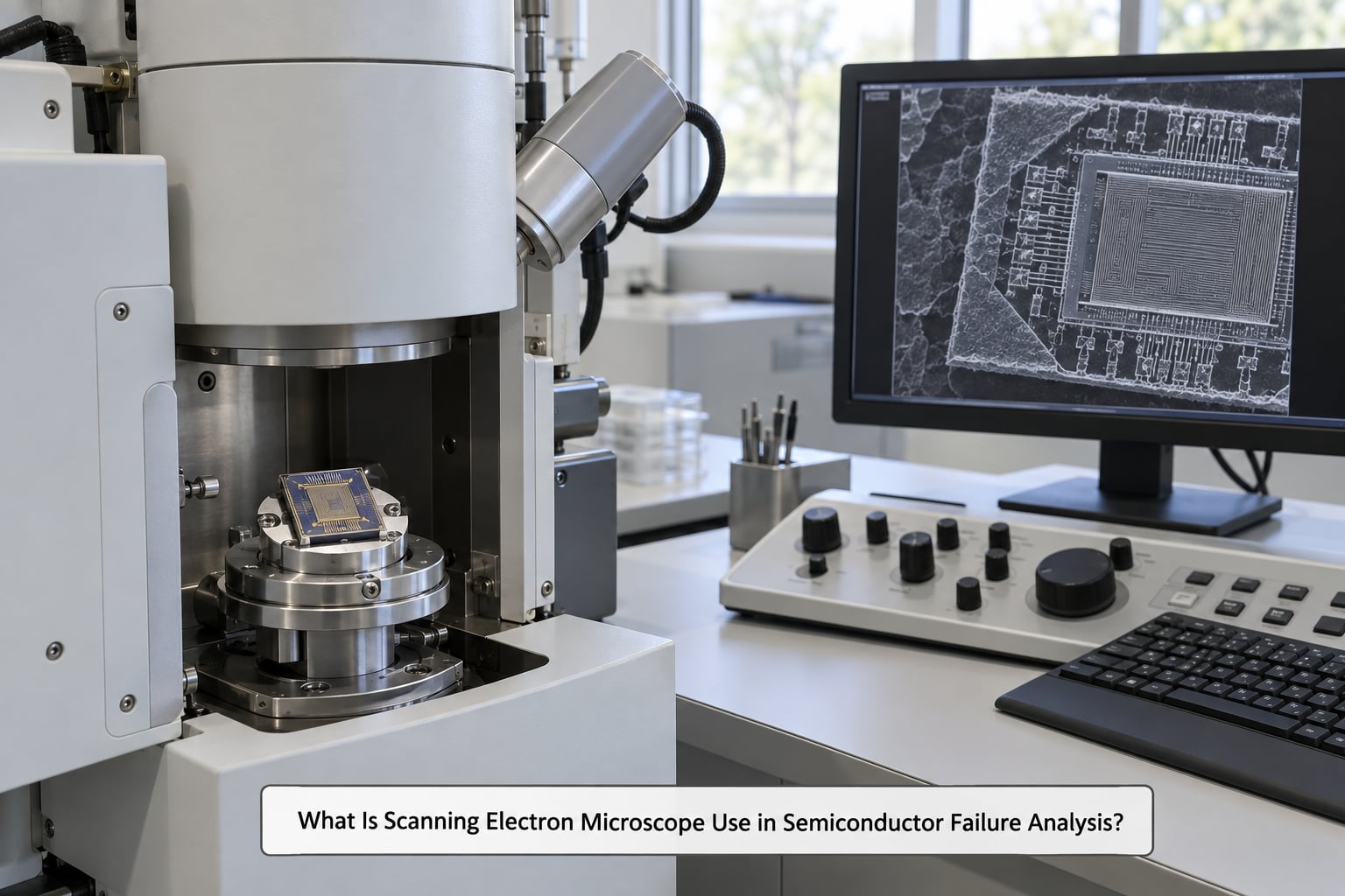
Scanning electron microscope use in semiconductor failure analysis means using a focused electron beam to image a failed device at nanometre scale, first to localise the defect and then to characterise it. The electron beam is raster-scanned across the sample inside a vacuum, and the signals emitted at each point are collected to build an image. Secondary electrons give surface topography. Backscattered electrons give composition contrast by atomic number. An integrated X-ray detector picks up characteristic X-rays so you can map which elements are present.
The same instrument answers a second family of questions. With the device biased under the beam, voltage contrast reveals electrically open or shorted structures while the part is still live. With cathodoluminescence or electron-beam-induced current detection, you can find where charge is actually collected or where carriers recombine. Those modes turn an SEM from a surface camera into an electrical localisation tool.
Here is what it does not do, and this matters when you scope a study. An SEM does not pass or fail a device on its own, it does not detect a defect buried under opaque material without preparation, and it is blind to anything deeper than the depth of field it can resolve at the working distance you chose. It is one instrument inside a flow.
How SEM differs from the other tools you already own
Optical microscopy is faster, cheaper and non-destructive, and it stays useful on every packaged part. It runs out of resolution around a micrometre, which is well above the feature sizes that matter on a modern logic or memory device.
Electrical characterisation measures the fault precisely but cannot see it. Curve tracers, transient latch-up tests and nanoprobing give you the resistance, leakage and capacitance behaviour that define the failure.
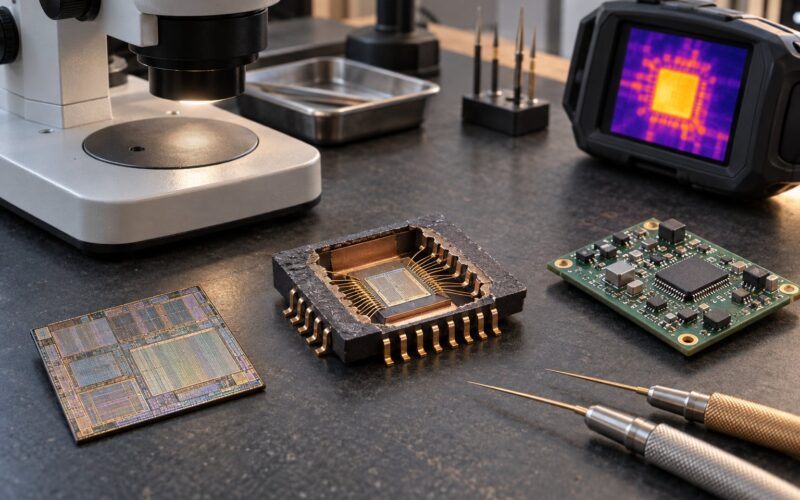
Thermal and emission methods find where the energy is going, which usually narrows the search to a region rather than a defect. The SEM then goes to that region and shows the structure.
A quick definition for the record
A scanning electron microscope is an instrument that focuses a beam of electrons onto a sample in vacuum and forms an image from electrons scattered or emitted by that sample. A field emission gun, or FEG, produces a narrow bright beam that makes the resolution figures worth quoting. For failure analysis work, the practical resolution is usually set by the size of the defect you need to see, not by the instrument specification on the data sheet.
Why SEM Is Used in Semiconductor Failure Analysis
Devices now hide failures in places that optical inspection cannot follow. Interconnect stacks sit under low-kV dielectrics, memory arrays place active layers above logic, and advanced packages add hybrid bonds, micro-bumps and fan-out redistribution layers. Each buried interface is a place where a void, a crack, a delamination or a contaminated surface can form, and each is invisible from the outside.
The evidence SEM produces falls into a few families, and a good report uses more than one.
Surface morphology
Secondary electron imaging shows the topography of the die surface and of the die after de-cap. Melted metal from an electrical overshoot, cracked passivation, lifted bond wires, missing bump material and fractured pad edges all show up as shape before they show up as chemistry.
Cross-sectional structure
Cross-sectioning turns the device into a stack you can read. You see where a metal line thinned, whether a dielectric delaminated from the metal beneath it, whether a via is properly filled, and whether a bond interface contains a void or an unreacted layer.
Particles, residues and contamination
Backscattered contrast plus EDS maps answer whether the bright speck on a pad is a metal fragment from the tool, a mould compound filler, a fibre from the assembly line or a genuine part of the design. This is one of the highest-yield SEM applications in incoming inspection and in yield-excursion work.
Breaks, cracks and mechanical damage
Package cracking, board flex damage during assembly, and handler overstress all leave physical signatures. A crack that runs from a corner of the die to a specific bond pad is a very different failure from a crack that runs through a random metallisation line.
Electrical context
Voltage contrast, electron-beam-induced current and cathodoluminescence show which structures are still connected. On a device with thousands of identical lines, that is the difference between finding the one open in an afternoon and not finding it at all.
How SEM Imaging Works for Semiconductor Devices
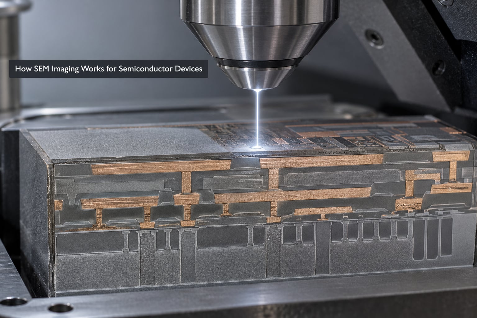
Everything in the column exists to put a small, bright, controllable beam on one spot and to collect what comes back. A field emission gun emits electrons that are shaped by electromagnetic lenses, accelerated through the anode aperture and focused to a spot on the sample. Raster deflection sweeps that spot line by line while the detector signal builds the image pixel by pixel.
Secondary electron imaging, the default mode
Secondary electrons are low-energy electrons emitted from the top few nanometres of the surface. Their yield depends strongly on the angle between the surface and the detector, so SE images read almost like a lighting effect. Everything in view is in focus across a large depth of field, which is why SE is the mode for topography, for particles, and for the fracture surfaces analysts photograph.
Backscattered electron imaging, the composition mode
Backscattered electrons come from deeper in the sample and their yield rises with atomic number. Heavier elements scatter more, so a tungsten contact looks brighter than aluminium beside it, and a copper particle in an oxide matrix pops out. It is the quickest way to find where the different material families are.
In-column detection and low-kV contrast
An in-column detector sits inside the pole piece, which improves collection efficiency and signal-to-noise at low beam energy. That matters on modern devices, because low landing energy limits how far the beam penetrates and therefore how much the volume above the feature charges. Lower energy, shorter penetration, less charging.
Choosing the landing energy
Resolution and charging pull in opposite directions. The old rule of thumb still holds: a useful spatial resolution figure is roughly a third to a half of the beam landing energy expressed in electron volts. A 1 kV landing energy therefore gives you usable detail around a few tenths of a nanometre, a 5 kV landing energy around a nanometre, and a 15 kV landing energy around a few nanometres at best.
You do not always want the finest resolution available. Higher energy means more signal for EDS, better contrast from deep bulk effects, and less time dwelling on a beam-sensitive area. For a cross-sectioned lamella, working at the lowest energy that still resolves the feature usually costs nothing.
| Target | Landing energy range | Preparation |
|---|---|---|
| Surface particle or residue on a die | 1 to 5 kV | De-cap, optional conductive coat |
| Shallow metal interconnect | 3 to 5 kV | Delayer or polish |
| Full cross-section including buried BEOL and FEOL | 10 to 20 kV | FIB lamella or broad-beam polished section |
| Package interface, bond pad or mould surface | 5 to 10 kV | Cross-section, possible carbon or gold coat |
Vacuum and charging
Standard SEM imaging runs in high vacuum, usually around 10 to 5 Pa, and any insulating region accumulates negative charge under the beam and deflects the image. On modern logic devices with low-kV dielectrics, this is the single most common reason a good session produces unusable images.
Environmental SEM instruments run at higher pressure with a gas present, so charge is neutralised continuously by ionising the gas. Low-vacuum imaging is also used on delayered samples when the evidence is already captured and the analyst accepts the resolution trade-off. A conductive coating works too, but on a device you may be painting over the very residue you came to identify.
How to Prepare Semiconductor Samples for SEM Analysis
Sample preparation decides whether the analysis succeeds. You can have the best instrument on site and still destroy the evidence before you reach it, and preparation is the only irreversible part of the flow. Everything before it is repeatable.
Start from the electrical data, not from the microscope
Pick the point of interest from the failure signature. If the part shows a resistive open, you have a candidate list of opens. If it shows leakage or a short, you are looking at dielectric damage, bridging or a contaminated surface. Bring that hypothesis into the sample-prep plan, because it decides which layers you need to expose.
De-cap before anything else
Mould compound and the die attach epoxy have to come off first. Wet chemical etching with the correct solvents, or laser or plasma ablation, keeps the surface clean. Too aggressive a mechanical approach leaves smeared metal that will be mistaken for a defect later.
De-layer deliberately
Delayering removes passivation or dielectric so you can reach a metal line. It is done by wet etch, reactive ion etch or laser. Each method has a signature: wet etch can undercut and leave rounded metal edges, reactive ion etch can leave polymers on the sidewall, and laser ablation can melt or spatter the metal at the point of interest. Record which one you used, because the analyst reading the image will want to know.
Cross-section by polishing or by FIB
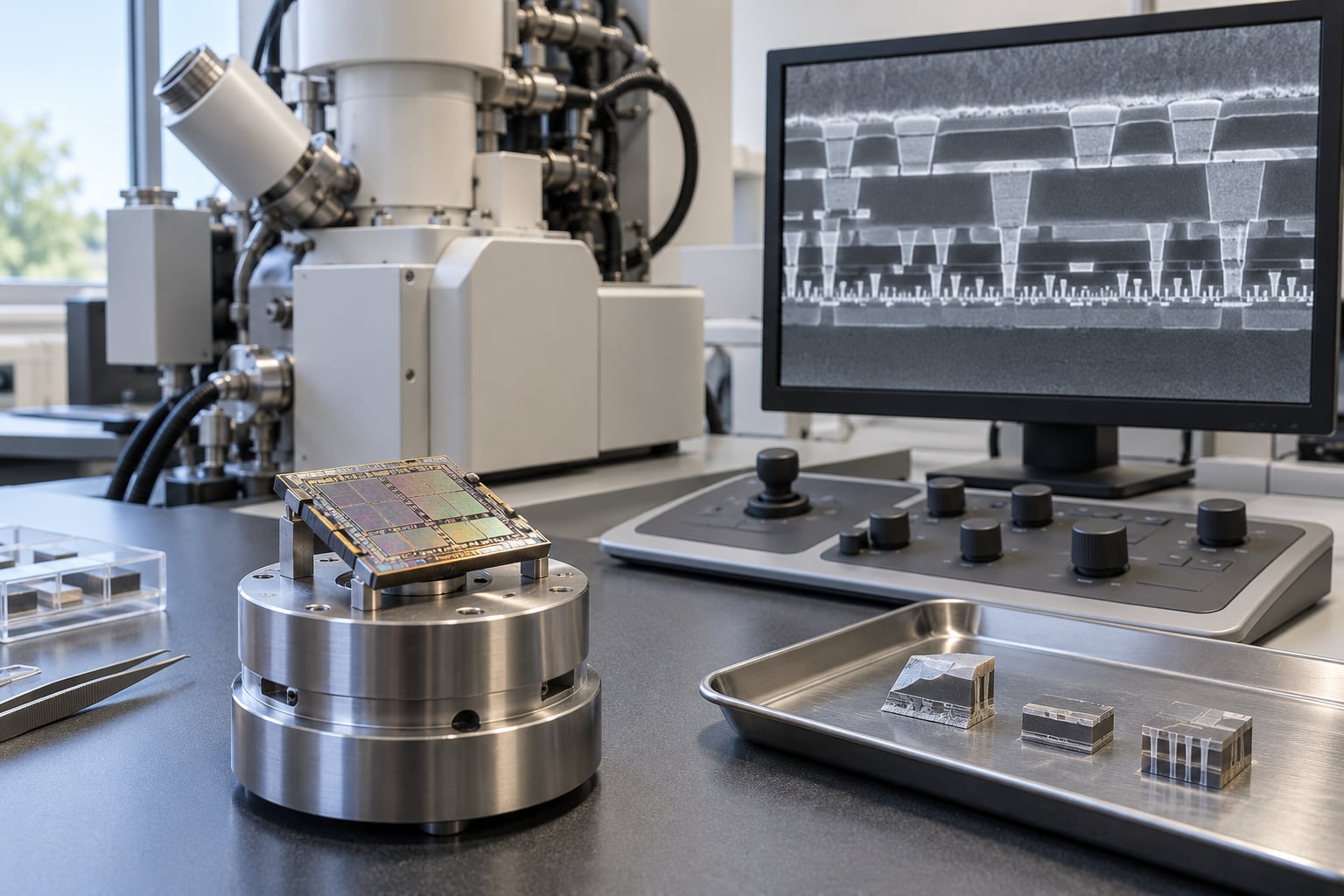
The two routes answer the same question at different scales. A broad argon ion beam can mill a section more than a millimetre wide, which suits package and board-level work where you need to see a long stretch of interconnect in one frame, but the finish and the redeposition are rougher than a narrow FIB section. A focused ion beam prepares a thin lamella, typically tens to a few hundred nanometres thick, through a chosen point, with far better placement control and much better depth of field for high-resolution imaging.
FIB has its own artefacts. Gallium implantation at the surfaces, redeposition of sputtered material onto nearby features, curtaining on the cut face and curtaining-free milling trades against milling time. Analysts argue about these constantly, and the practical rule is to mill a slightly larger region than you think you need, then take the final image from an area away from the corners.
Polish-damage is the artefact analysts under-rate. Mechanical grinding and final ion polish push material sideways and can smear a soft metal over an adjacent dielectric. If you ever see a layer that appears to bulge into its neighbour, suspect the preparation before you suspect the process.
Mount, ground and coat
Mount the sample so it is electrically connected, because a floating conductor on an insulating stage will charge instantly. Carbon tape works for routine work; conductive paint or a bonded stage contact is better when you need beam-stable conditions. Then coat only if you must. A thin carbon or gold layer, roughly a few nanometres, stabilises the surface but blurs the finest detail and adds its own peaks to the EDS spectrum, so subtract it during interpretation.
Cross-sections usually need the coating more than an intact die does, because the cut face exposes a large area of material with no native ground path.
How to Interpret SEM Images and Distinguish Common Defects
Reading a micrograph is a two-step process. First work out what the contrast means, which depends on the detector you used. Then match the morphology to a known mechanism. Doing it the other way round is how analysts convince themselves they have found a root cause.
Contrast tells you what you are looking at
Bright in SE means a surface tilted towards the detector. Bright in BSE usually means heavier element, or simply a denser region. Flat and featureless can mean the opposite of undamaged: a sputtered or etched surface has no topography to show, so an apparently clean region may be one you have already altered during preparation.
On a cross-section, the metal stack shows up clearly by composition contrast while the low-kV dielectric around it stays dark. That contrast pattern is what lets you see a thinning line, a lifted interface or a void between layers.
Open circuits
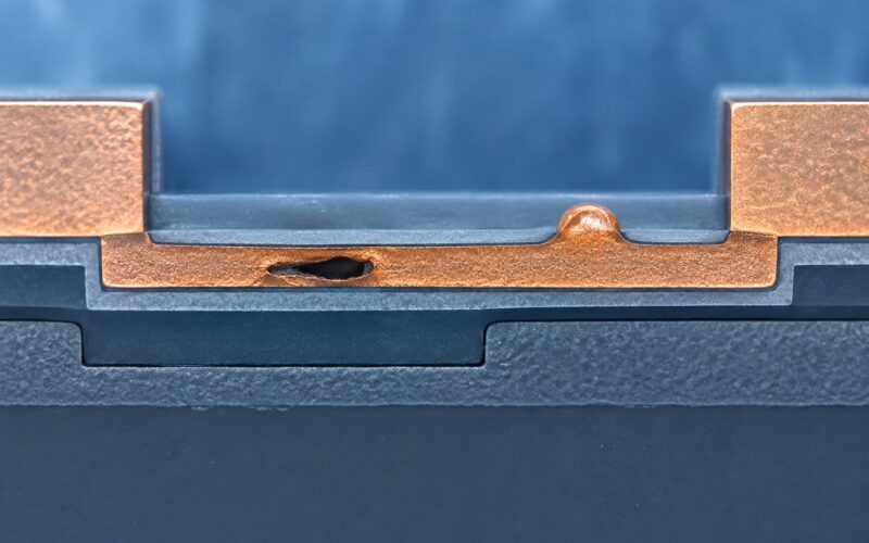
A void in a via or a break in a line shows as a gap in the metal and a change in BSE brightness across the gap. On a live device, voltage contrast is faster: an unbroken line that carries no bias appears dark or bright depending on the detector, while a broken line stands out sharply. Anti-fuse and fusible-link blowouts show as fused, recrystallised metal with a much wider grain structure than the surrounding line.
Shorts and bridging
Bridging shows as a continuous bridge of one material across what should be empty space. Ionised metal from a plasma etch often gives a distinctive fluffy, dendritic texture. Dendritic growth between a biased line and a neighbouring ground line is a real failure mode in humid environments and shows up directly in SE.
Electromigration and stress migration
Electromigration voids appear inside the line, roughly centred in its width, and stress migration voids appear at the edge of the line near the interface. The distinction matters because it points at different process problems: electromigration is current density and temperature, stress migration is thermal-expansion mismatch in the stack.
Dielectric breakdown
Low-kV dielectrics do not melt the way metal does. They show a carbonised crater, a rounded rim and often a path of small voids leading to a via or an edge, which is the signature of repeated partial discharge. Look for the crater, then look for why the field concentrated there.
Corrosion and moisture ingress
Corrosion products give a soft, rounded, low-contrast appearance and frequently carry elements that have no business in the device, such as chlorine, sodium or copper at unexpected sites. EDS is what turns a suspicion into a finding here.
Packaging defects and mechanical damage
Delamination shows as a lifted layer with a dark gap underneath, which BSE contrast confirms by the lack of any signal across the interface. Bond pull failures leave a partial pad impression. Micro-bump cracking from thermo-mechanical cycling appears as a crack running through the bump, usually at the narrowest point.
Contamination
EDS is the fastest path to naming a particle. The rule is to check whether the spectrum contains elements that cannot belong to the process at that point in the flow. A copper-rich particle on a die pad at wafer test points to a tool or handling step, and that is a yield action rather than a device action.
How SEM Analysis Supports Root-Cause Analysis
A micrograph on its own is a description. Root cause comes from correlating the description with everything else you know about the part, and the discipline analysts need most here is resisting the urge to stop at the first thing that looks wrong.
Correlate with the electrical signature
Avoid found at a single via is consistent with a weak single defect. The same via type broken on every instance of one part number points to process. If the electrical test shows a specific resistance change rather than a clean open, that constrains which of the physical defects you are willing to accept as the cause.
Correlate with process and test history
Ask what changed. A wafer lot, a build of the package, a change of assembly house, a new test handler, a different flux or mould compound lot. Failure analysis that ignores process history often re-discovers a known issue that someone has already closed out. Time at temperature under bias, a specific voltage step and a specific humidity condition all shape which signature you should expect.
Correlate with package construction
The same void morphology means different things in different stacks. A gap under a die attach is a different problem from a gap between two redistribution layers. Read the package design, the intended stress buffer and the stack-up before assigning a mechanism.
Separate cause from secondary damage
This is the most common analytical error. An electrical overstress melts a bond wire, and the melted wire then shorts two pads, and the analyst reports the short. The short is a consequence. Rule of thumb: check whether the damage timeline is consistent with the failure mode you are claiming. Melt recrystallisation, exploded anti-fuses and cracked ceramics all point to an energy event that happened once, early, and should make you look for its origin rather than at the worst-looking site.
Close the loop
The last step is as important as the imaging. A confirmed root cause has to reach the process or design owner in a form they can act on: the defect class, the mechanism, the layer and tool step it implies, and whether other parts from the same lot are at risk. That is the deliverable that makes the SEM work worth paying for.
SEM Versus Other Semiconductor Failure-Analysis Methods
Almost every question about the SEM comes down to what else is on the bench. The table below sets out the main candidates honestly, because the right answer is rarely “use the SEM”.
| Technique | Typical resolution | Destructive? | Best question it answers |
|---|---|---|---|
| Optical microscopy | About 1 micrometre and down with high-NA objectives | No | Is there visible external damage, and where is it? |
| EMMI and InGaAs-EMMI | Spot of a few micrometres, set by laser or optics | No | Where is the emitting or hot site on a biased part? |
| OBIRCH | Typically a few micrometres, set by laser spot size | No | Which line shows a resistance change under local heating? |
| Scanning acoustic microscopy | Micrometre to submicrometre in the depth direction | No | Is there delamination, voiding or a package crack under the surface? |
| X-ray microscopy (XRM) | Submicrometre, through the full package depth | No | What does the 3D internal structure look like before anything is cut? |
| SEM | About 1 to 10 nm at the surface; deeper features with higher energy | Usually, for prepared sections | What exactly is at the failure site, and what is it made of? |
| FIB-SEM dual beam | SEM resolution, with precise site selection | Yes | What is the cross-section at this exact point? |
| TEM and STEM | Below 1 nm, often atomic | Yes | What is the interface or layer structure at atomic scale? |
| Nanoprobing and curve tracing | Not imaging | Gently, on a prepared device | What is the electrical value at this node? |
Optical versus SEM
Optical wins on speed and on intact parts, and it should always run first. SEM wins the moment the answer depends on a nanoscale feature or on elemental identity. Neither replaces the other; optical localises cheaply and the SEM confirms.
Emission-based methods versus SEM
EMMI detects visible and near-infrared photons from a biased device, typically across roughly 350 to 1100 nm, which suits gate oxide defects, junction leakage, latch-up and ESD damage. InGaAs-EMMI extends to roughly 900 to 1700 nm, where it is reported to be several times faster and more sensitive than visible EMMI because silicon emission is stronger in that band. OBIRCH focuses an infrared laser on a spot and looks for a change in the line resistance as the spot heats the conductor, which finds local defects in a specific current path.
These methods find a location without consuming the sample, which is exactly why they run before the SEM. The community complaint that they are hard to compare across labs is fair, because each lab markets its own combination of detectors and laser spot sizes.
XRM versus SEM
X-ray microscopy sees through a whole package without cutting anything, which makes it the natural first pass on fan-out wafer-level packaging, hybrid bonding and stacked memory where the suspect interface is anywhere in a millimetre-scale volume. Its weakness is contrast and its weakness is resolution: it will show you a void where to stop looking, and then the SEM shows you what the void is.
FIB-SEM versus SEM
A standalone SEM needs a pre-made sample. A dual-beam FIB-SEM adds a focused ion beam that mills in the same chamber, so you can move to a known coordinate, cut at it and image the fresh face without ever leaving vacuum. That is why most modern FA labs run a dual beam for preparation and finish on the electron column.
SEM versus TEM
Use TEM when the question is about the atomic structure of a thin interface: the thickness of a barrier, whether a bond is truly dense, the profile of a junction. Use SEM for everything from the whole die down to a few tens of nanometres, plus elemental mapping. TEM wins on resolution, loses on field of view and sampling, and demands a much thinner, more delicate lamella.
What Are the Limitations and Common Mistakes in SEM Analysis?
The most-searched question about this instrument is the one most competitors avoid. The downsides of using a scanning electron microscope are real, they are well understood, and every one of them has a documented mitigation.
Charging
The primary limitation. An insulating region deflects the beam and the image smears, shifts or goes black. It gets worse at higher landing energy and worse as devices add low-kV dielectric. Mitigation is lower energy, shorter dwell, a conductive coating, bonded grounding, or environmental SEM imaging.
Beam damage
Electron beams can polymerise resist, reduce or re-oxidise thin oxides, and change beam-sensitive materials while you watch. On a wide-bandgap device, a charge or an injected carrier can also create a feature that is not a manufacturing defect. Lower energy, shorter exposure and acquiring your damage-prone evidence first all reduce the risk.
Sample preparation artefacts
Polishing smear, redeposition from ion milling, gallium implantation at the lamella surfaces, curtaining, and delayer damage are all placed on the sample by the analyst. Each one can look exactly like a defect. This is the largest single source of false root causes in failure analysis.
Surface information only
An SEM without cross-sectioning answers questions about the surface. Analysts routinely underestimate how much destructive preparation a study needs, and discovering that at the end of a stream costs time.
Contamination and drift
A hydrocarbon layer grows on the beam path during long sessions and drifts the image, which is a real issue when comparing a known-good device against a failed one over several days. Clean the column, use a low-contamination vacuum and, where the question demands it, use a fresh, clean chamber.
Common mistakes in practice
- Believing one image. A single frame at high magnification can be a coincidence of angle, contrast setting or charging. Move the stage and confirm the feature twice.
- Losing the scale bar and the conditions. A micrograph without a scale, magnification, detector, landing energy and working distance cannot be reviewed by anyone else.
- Ignoring the sample history. Which solvent, which etch, which ion beam, how long ago. If it is not written down, the evidence degrades.
- Coating over the target. A conductive layer is a compromise, not a default.
- Over-interpreting EDX numbers. Quantification is only as good as the standard, the matrix correction and the fact that the interaction volume may be larger than the feature you are measuring.
- Stopping at the physical site. A confirmed defect that never reaches the process owner leaves the yield problem where it was.
Frequently Asked Questions
What does SEM reveal in semiconductor failure analysis?
SEM imaging shows surface topography in secondary electron mode and composition contrast in backscattered electron mode, so an analyst can see voids, cracks, delamination, broken interconnects, foreign particles and residue directly. With EDS it adds elemental identification, and with voltage contrast, EBIC or cathodoluminescence on a biased device it shows which structures are still electrically connected. It is normally the confirmation step after electrical data and optical or emission imaging have narrowed the search.
How should a semiconductor die be prepared for SEM imaging?
Work from the electrical signature rather than the microscope. De-cap the package first, then delayer or cross-section to reach the suspected layer, choosing wet etch, reactive ion etch, laser or broad ion milling based on the depth you need and how much surface damage you can accept. Mount the sample with a ground connection, coat only when charging demands it, and record every preparation step so the image can be interpreted later.
Can SEM identify electrical opens and shorts in an IC?
Yes, with the right mode and the right preparation. On a live device, voltage contrast makes an open line stand out against thousands of intact ones, which is often faster than cross-sectioning to check each candidate. For shorts, bridging between features is visible in SE and BSE, and EDS confirms whether the bridge is metal from the process or contamination from outside it. Cross-sectioning is still needed to see the buried cause.
When is cross-sectioning necessary for semiconductor failure analysis?
Cross-section when the defect is buried, when the failure is inside the interconnect stack rather than on the die surface, or when you need to relate the observed anomaly to the layer beneath it. A broad ion beam can mill a section more than a millimetre wide for package-level work, while a FIB lamella gives far better placement control and higher resolution at the cost of a smaller field of view. Start non-destructive whenever the part allows it.
Is SEM better than optical microscopy for failure analysis?
Neither is better; they answer different questions and are used in order. Optical inspection is fast, non-destructive and the right first pass on an intact part, but it runs out of useful detail at features above about a micrometre. SEM resolves nanometre-scale structure and adds elemental analysis, at the cost of vacuum, preparation for sectioned samples, charging and beam damage. Most studies use both, optical to localise and SEM to confirm.
What information should accompany SEM images in a failure-analysis report?
Every micrograph needs a scale bar, magnification, detector type, landing energy, working distance, coating and a statement of the sample history, including which de-cap, etch or ion-milling step exposed the surface. Alongside that, report the electrical data that led to the site, any comparison images from known-good parts, the EDS conditions, and your interpretation with the reasoning that separates the primary failure from secondary damage.
Conclusion: Start with the Failure, Then Choose the Right Imaging Evidence
The SEM is a confirmation instrument, not a starting point. Define the failure from the electrical data first, preserve the part before anything destructive happens, and localise with the least invasive method that can do the job: optical, then emission-based or thermal, then cross-section. Only then pick the microscopy mode and the landing energy that answer the question.
Interpret every image with process context attached, and separate the primary failure from the damage it caused on the way out. If the imaging cannot be reproduced by someone else six months later, it did not happen, regardless of how good it looked.