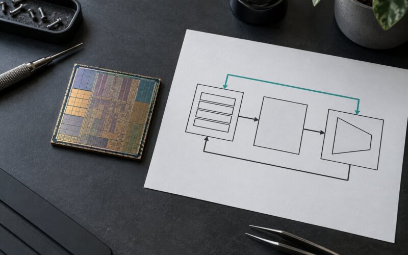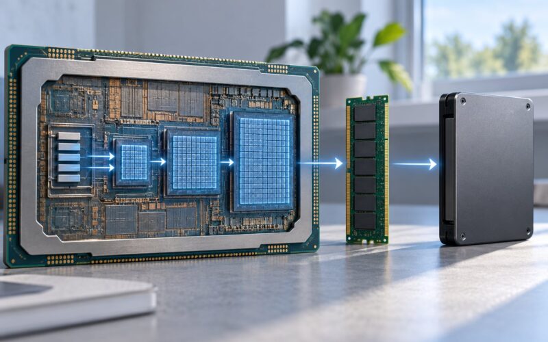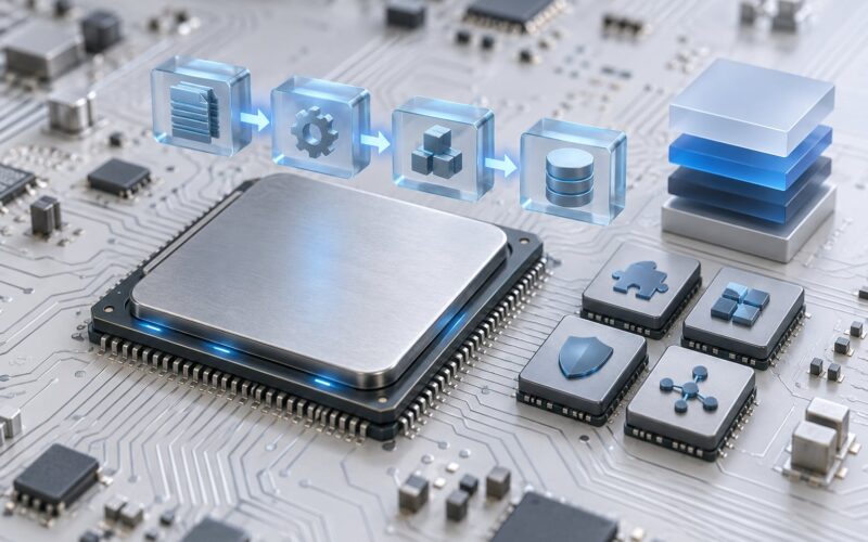
How AI accelerators are designed comes down to one loop: profile the workload, map it onto hardware that can feed the arithmetic, and cut the cost of moving data. Modern neural networks spend almost all their time doing multiply-accumulate on large matrices, so a general-purpose processor spends most of its time waiting on memory instead. An accelerator removes that wait by building thousands of parallel arithmetic paths, keeping weights physically close to them, and dropping numeric precision the model does not actually need.
The catch is that every one of those decisions narrows what the chip can do later. A design that nails one model class can be useless the following year, and a design that stays flexible pays for it in power. What follows is the flow I would walk through as a chip engineer, from profiling the workload on day one to bringing the part back from the fab on day three of the schedule.
Table of Contents
- What Is an AI Accelerator?
- How AI Workloads Shape the Architecture
- How AI Accelerators Are Designed: From Workload to Dataflow
- Compute Units for Matrix and Neural Operations
- Memory Architecture and Bandwidth
- Interconnects and Multi-Core Scaling
- Power, Performance, and Area Tradeoffs
- Memory, I/O, and Packaging Choices
- Verification, Software, and Making the Accelerator Usable
- A Complete AI Accelerator Design Example
- Frequently Asked Questions
- How does an AI accelerator work?
- How are AI accelerators designed step by step?
- What is the difference between a GPU and an AI accelerator ASIC?
- Why do AI accelerators use high bandwidth memory instead of ordinary DRAM?
- Is an AI accelerator designed for one model or for many?
- How do you verify an AI accelerator design before tapeout?
- Conclusion: Where to Start
What Is an AI Accelerator?
An AI accelerator is a processor built specifically to run neural network math faster and more efficiently than a general-purpose CPU. It does that with three structural choices: wide parallel execution of multiply-accumulate (MAC) work, on-chip memory arranged so data is reused rather than refetched, and hardware support for low-precision number formats such as BF16, FP8, and INT8.
CPUs are built for low latency on complex, unpredictable instructions. Deep learning has the opposite profile: enormous, regular, data-parallel work where one stall matters less than how many operations finish per second per watt. That mismatch is the entire reason accelerators exist, and it is why the same chip can be excellent at one and useless at the other.
| Accelerator type | How it runs work | Precision sweet spot | Typical memory path | Flexibility | Best fit |
|---|---|---|---|---|---|
| Data center GPU | Thousands of threads, SIMT lanes, cached loads | FP16/BF16/FP8 | HBM plus large L2 | High | Training and fast-changing model research |
| TPU-style ASIC | Fixed matrix engine with scheduled dataflow | BF16/FP8/INT8 | HBM, mostly streaming | Medium | Hyperscale training and inference fleets |
| Custom accelerator ASIC | Spatial dataflow mapped to an operator graph | INT8/INT4 usually | On-chip SRAM plus HBM or LPDDR | Low to medium | Fixed workloads where volume justifies NRE |
| NPU in an SoC | Small block of MACs shared with CPU and GPU | INT8/INT4 | Shared system DRAM, small SRAM | Low | On-device inference, always-on sensor paths |
| FPGA | Reconfigurable fabric and hard DSP blocks | FP32/FP16/INT8 | DSP blocks, block RAM, external DDR | Very high | Prototyping, low-volume, changing standards |
| Wafer-scale engine | Single die-sized fabric of cores and local SRAM | FP16/BF16 | Distributed SRAM plus a few HBM stacks | Medium | Models too large to fit in one socket |
Two workload families pull the design in different directions. Training is throughput-bound, runs large batches, tolerates days of runtime, and needs precision high enough that gradients do not vanish. Inference is dominated by latency and cost per query; for autoregressive text generation, each new token reads the entire model once, so the chip spends most of its life waiting on memory bandwidth rather than computing.
How AI Workloads Shape the Architecture
Workload characteristics decide the architecture before anyone draws a block diagram. The operator mix sets the compute mix, the tensor shapes set the tiling, and the tolerance for accuracy loss sets the numeric formats. Batch size and latency targets decide whether you are building a throughput machine or a response-time machine.
A transformer inference pass is a useful example of how quickly assumptions break. Prefill, where the whole prompt is processed at once, is compute-bound and rewards a wide matrix engine. Decode, where one token is generated at a time, is memory-bound: arithmetic intensity collapses, and adding more MACs changes almost nothing while adding bandwidth changes everything. The same chip serves both, but the two phases stress it in opposite directions.
Attention adds two more constraints. Its cost grows with the square of sequence length, so a chip aimed at long-context work needs larger scratchpads for activations and a smarter streaming pattern for the key-value cache. Mixture-of-experts models add a third: the weight matrices are huge but only a few are touched per token, which makes routing, index bookkeeping, and scatter-gather bandwidth first-class hardware concerns rather than software details.
How AI Accelerators Are Designed: From Workload to Dataflow
The design process is iterative, and each pass moves between a model of the workload, a model of the machine, and RTL. A workable sequence looks like this.
- Profile a real workload, not a synthetic one. Capture instruction mix, tensor shapes, arithmetic intensity, and memory access patterns from the models you expect to run, including the awkward cases: short sequences, batch size one, cold caches.
- Fix the numeric contract. Decide which formats ship in hardware, what the accuracy loss budget is per layer, and whether a host-side rescaling step is allowed. This decision constrains the array design more than any other.
- Build a performance and power model before RTL. Use a cycle-accurate or trace-driven simulator to project time, energy per operation, and die area. If the model says the design misses its target, changing a block diagram costs nothing.
- Choose the dataflow architecture. Systolic, spatial dataflow, or a SIMT-like schedule. The choice decides where buffers live, how operands move, and how tolerant the design is to unfamiliar operators.
- Design the memory hierarchy around reuse. Size the scratchpads from working-set analysis, then pick how many HBM channels and what precision of DRAM feed them.
- Size arrays and pipelines from the model. Number of MAC elements, vector width, issue width, and clock target all come out of the roofline analysis rather than out of marketing numbers.
- Iterate against power, area, and thermal limits. Re-run the model after each block change, then re-run it after physical design, because placement moves power and timing far more than the RTL does.
Engineers coming from general-purpose design often underestimate steps 3 and 7. A block diagram that looks 20 percent fast on paper routinely loses that margin to routing congestion, clock skew, and IR drop once real macros are placed.
Compute Units for Matrix and Neural Operations
Compute in an AI accelerator is built from multiply-accumulate elements, and the interesting design work is in how they are arranged and fed. A MAC element takes two operands, multiplies them, and adds the result to an accumulator. One MAC is trivial. What matters is how thousands of them get operands without stalling.
A systolic array is the classic answer. It is a regular grid of processing elements that pass partial sums to their neighbours on a fixed schedule, so data moves in a rhythm and the control logic stays tiny. Because the shape is fixed, the compiler must tile and reorder operations to fit the array’s dimensions, which is exactly why these designs have limited operator flexibility. Row-stationary, weight-stationary, and output-stationary variants differ in which operand each element holds, and each suits a different layer shape.
Dataflow and spatial designs take a different approach: a fabric of simple compute tiles connected by a network, with data routed to wherever it is needed. That handles irregular shapes and sparsity better, at the cost of a much more complicated compiler and interconnect. Reconfigurable-array designs, often called CGRAs, sit in between, giving compilers a two-dimensional space of candidate mappings rather than one fixed schedule.
Transformer inference also needs vector hardware, not just matrix hardware. Softmax, layer norm, activation functions, and rotary position encoding are elementwise or reduction operations that a MAC array handles badly. Most production accelerators therefore pair a matrix engine with separate vector pipelines and route work between them on chip, so a layer fusion happens in a local buffer rather than in a round trip to DRAM.
Format support is a hardware decision with a software cost. Every additional format means a second multiplier width, a different rounding and saturation path, and another quantization recipe to validate. Most designs ship a training format, a wide format for accumulators, and one or two inference formats, and they make everything else the compiler’s problem.
Memory Architecture and Bandwidth
Memory is where most accelerator design arguments end up. The arithmetic is comparatively easy; the hard part is getting every weight and activation to the right place on time without paying for it three times. Moving a 32-bit word out of DRAM can cost one to two orders of magnitude more energy than the MAC operation it feeds, which is why data movement, not multiplication, dominates the energy bill.
| Level | Typical size on one accelerator | Access latency | Role |
|---|---|---|---|
| Registers | Hundreds of thousands across the die | 1 to a few cycles | Holds operands currently being multiplied |
| SRAM scratchpad or tensor memory | Tens of megabytes, distributed per compute cluster | Tens of cycles | Feeds the arrays and holds fused intermediate results |
| On-chip cache | Several megabytes, shared | Dozens to a few hundred cycles | Absorbs repeated access to weights and activations |
| HBM | Tens of gigabytes per package, a few stacks | Several hundred cycles | Holds weights that do not fit on die |
| DDR or LPDDR | Gigabytes to tens of gigabytes | Hundreds of cycles plus refresh stalls | Host memory and capacity tier in edge parts |
Most designs use a managed scratchpad rather than a classic cache for the working set feeding the arrays, because software knows the tile schedule and the cache does not. The programmer, in practice the compiler, tells the hardware exactly when to prefetch the next tile and when to double-buffer, and the memory controller simply keeps the wide pipe full.
Bandwidth and capacity trade against each other. HBM stacks deliver aggregate bandwidth in the terabytes-per-second range per package, but the wide parallel interface costs significant die area in the memory controller and routing, and it is the single most constrained resource in a large AI chip floorplan. Designs that need more bandwidth than HBM can supply either add stacks and live with the area and power cost, or restructure the workload so it moves less.
For decoder-style inference, the key-value cache is the memory problem that decides the product. It grows linearly with batch size and context length, is read once per token, and is written every layer. Keeping it in HBM costs bandwidth; keeping it in on-chip SRAM costs capacity; the design usually splits the batch, holding the hot recent portion on die and the remainder in HBM.
Interconnects and Multi-Core Scaling
A single accelerator rarely holds the model or the throughput target, so most designs ship as a cluster of devices. The interconnect decides how much of the chip stays busy during collective operations like all-reduce, and it splits into two jobs that people often conflate. Scale-up links connect devices that act like one machine, usually inside a rack or a board. Scale-out links connect racks that run distributed training jobs.
| Link | Role | What it is optimized for | Typical role in an AI system |
|---|---|---|---|
| PCIe | Host and device attachment | Low cost, low power, moderate latency | Bringing accelerators into a server |
| CXL | Coherent memory and device attachment | Cache coherency and memory sharing | Sharing host memory and expanding capacity |
| UALink | Scale-up | High bandwidth with low latency between accelerators | Tying processors into one coherent accelerator domain |
| Ultra Ethernet | Scale-out | Loss-tolerant throughput at rack scale | Connecting racks in a training job |
| UCIe and die-to-die | On-package | Very short reach, very high bandwidth per watt | Chiplet-to-chiplet traffic inside a package |
On-chip, the network-on-chip fabric carries most of the traffic inside the die and is where utilization is won or lost. Multicast-heavy broadcast patterns suit a crossbar; irregular all-to-all traffic suits a mesh with adaptive routing. The classic mistake is sizing the fabric for average traffic, when a single layer transition can saturate it and stall every cluster at once.
Parallelism strategy follows the model. Data parallelism replicates the model across devices and needs only all-reduce. Tensor parallelism splits individual matrix multiplies and needs very high bandwidth every layer. Pipeline parallelism splits layers and adds bubbles. Expert parallelism for mixture-of-experts models routes tokens to different devices, which turns a network problem into a latency problem, because an expert that misses a token by a few microseconds stalls the whole step.
Power, Performance, and Area Tradeoffs
Performance targets are stated in operations per second, but the design is really constrained by the roofline. The roofline model puts arithmetic intensity, operations per byte of memory traffic, on one axis and achievable bandwidth on the other. Any point under the roof is a memory problem, whatever the FLOP number says. Most accelerator design reviews are really roofline reviews with a schematic attached.
Three levers move a design under that roof. Locality through larger scratchpads and better tiling reduces bytes moved per operation. Lower precision cuts both the bytes and the math, because an INT8 MAC fits in a fraction of the area and energy of an FP32 one. Sparsity helps only when you can skip work without paying to discover what to skip, which is why compressed-sparse formats need hardware metadata and a predictable pattern behind them.
Clocks are a power lever engineers underestimate. Each frequency increase multiplies dynamic power, and a large accelerator spends most of its energy in data movement rather than in the MAC array, so the array can often run slower than the surrounding data path without hurting throughput. Dynamic voltage and frequency scaling, clock gating, and power gating the idle memories are the standard levers once the block diagram is fixed.
Area is the budget nobody wants to talk about. A die that is mostly memory controllers and routing will not meet its yield or power target no matter how good the array is. So the real negotiation is always the same: give the compute array more elements, give the memory system more bandwidth, or give the design more margin on timing and thermal.
Lower precision is a real tradeoff, not a free win. Narrowing a weight or activation format can push a layer’s output outside the range that downstream layers were trained to handle. That is why quantization-aware training exists, and why accuracy regression testing is treated as a first-class part of accelerator signoff rather than a step the software team runs later.
Memory, I/O, and Packaging Choices
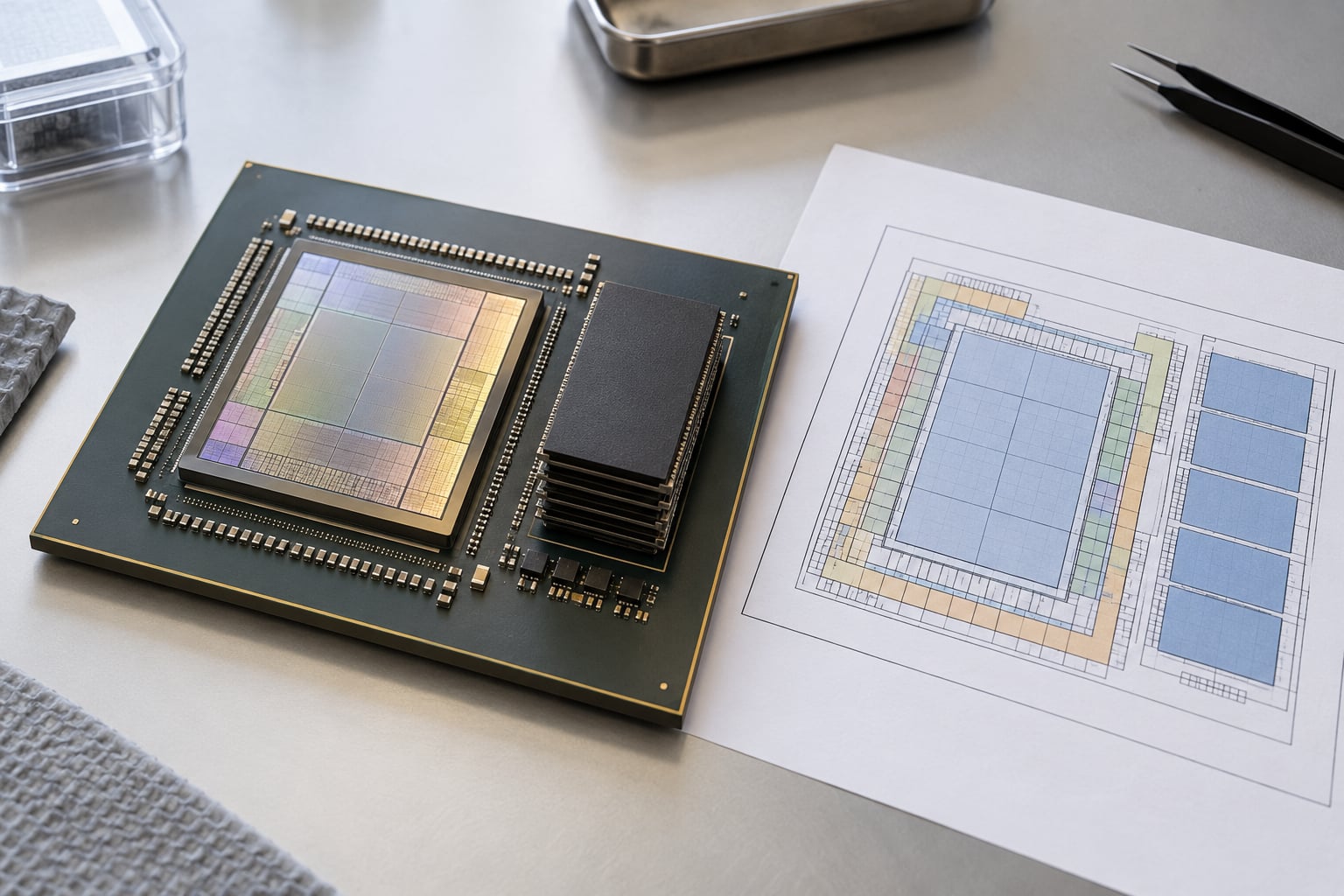
Packaging is no longer the last step of AI accelerator design. A modern AI package can hold a large compute die, several HBM stacks, and a set of chiplets, all on an interposer, and the arrangement of those pieces determines the power budget, the thermal design, and the yield economics of the whole product.
HBM stack count is the first decision. Each stack adds hundreds of gigabytes per second of bandwidth and a matching slice of memory controller area, but also adds power, heat, and package cost. Designs that can meet their bandwidth target with four stacks keep them, because the extra two rarely pay for themselves if the workload is compute-bound rather than memory-bound.
Chiplets change the arithmetic. Splitting a large design into a compute die and I/O dies lets each use the process node that suits it, enables mixing supplier processes, and cuts the cost of manufacturing a single enormous die. The price is a die-to-die interface that has to carry enormous traffic, plus the packaging and test work needed to make many known-good dies behave as one part. Foundries market this class of assembly as advanced 2.5D and 3D integration, and it is now routine for the largest accelerators.
Power delivery is the constraint that surprises people. An AI chip can draw hundreds of amps in bursts, which drives transient response through the package and interposer, not just average power. The power delivery network has to be designed as a physical structure with its own resistance and inductance budget, and a design that closes on average power can still fail droop at the array.
Thermal follows the same logic. Heat has to leave, and it leaves through a path of spreading, conduction, and convection or liquid flow. Everything above it, die thickness, the choice of a lower-resistance substrate, the power density per square millimetre, is a decision about how much heat the package can remove, not about how fast the logic is.
Verification, Software, and Making the Accelerator Usable
An accelerator is not finished when it tapes out. Verification and software are half the product, and both start long before the first netlist is stable.
Functional verification of a large accelerator is mostly a directed and constrained-random campaign plus a set of formal properties. The properties tend to be structural: no illegal data value reaches an array input, a buffer never overruns its index range, a scoreboard tracks every outstanding request. Clock-domain crossing and reset-domain crossing checks matter more here than in a small CPU because the chip is partitioned into many independently-clocked islands, and a single missed synchronizer shows up as rare corruption months later.
Design for test follows the same logic. Scan and ATPG cover the logic, memory BIST covers the SRAM banks and HBM interface paths, and the test plan has to assume that a full scan test of a billion-gate design takes hours, which shapes what you can afford to test at the factory versus at bring-up.
Emulation and FPGA prototyping bridge the gap before silicon exists. RTL simulation runs slow, so a trace of a real model that takes a second on target can take days to simulate. Emulation systems run the RTL on an FPGA array at a small fraction of real speed and are where a full model run usually happens for the first time. When bugs are found there, the team saves weeks at tapeout.
Synthesis and physical design are where the block diagram gets the final say. Floorplanning on an AI chip is dominated by the memory system, because the HBM controllers and their routing are the largest and most delay-critical structures. Place and route then trades clock frequency against power, and timing, power, and IR drop signoff close the loop. Expect a couple of engineering change orders after the first full-chip route; the goal is that they are small.
Software decides whether any of it gets used. The compiler stack, whether built on MLIR, Glow, or a traditional flow, maps a framework graph onto the dataflow the hardware supports, handles layout transforms, and schedules tiles. A runtime manages memory, picks kernels, and handles fallbacks. The frameworks underneath, PyTorch and TensorFlow among them, are where quantization-aware training and accuracy checking happen.
Measurement closes the loop. MLPerf Inference and MLPerf Training give a vendor-neutral way to compare parts, and roofline plots from hardware counters tell you which side of the roof a layer landed on. A design that hits its FLOP number but sits far under the memory roof is not finished, and the profiler is the only thing that tells you so.
A Complete AI Accelerator Design Example
Here is a worked example of how those decisions stack up. The target is a data center accelerator for decoder-style inference on a transformer with roughly 7 billion parameters, INT8 weights, a batch size of one, and a target of 30 tokens per second per user slot.
Step 1, the bottleneck. At 7 billion parameters and one byte per weight, the model is about 7 GB, and every generated token reads all of it once. At 1 TB/s of usable bandwidth, the floor is 7 milliseconds per token. Arithmetic for one token is about 14 GFLOP, so 30 tokens per second needs around 0.4 TFLOP/s, which a small array delivers easily. Decode is bandwidth-bound, and the design is now about memory, not compute.
Step 2, prefill changes the answer. Processing a thousand-token prompt in 100 milliseconds needs about 7 TFLOP, so the target rises to roughly 70 TOP/s at INT8. A compute array in the 50 to 100 TOP/s class with an INT16 accumulation path covers prefill and still streams the weights fast enough for decode.
Step 3, memory. The 7 GB of weights go in HBM, not on die, so the package carries four or more HBM stacks and the memory controllers take a large share of the die. A per-cluster SRAM of a few megabytes holds the tiled activations for one layer, and the key-value cache is split, with the hot portion on die and the rest streamed from HBM.
Step 4, compute. Because inference has a hard 8-bit weight path and small batches, the design is dominated by weight-stationary systolic tiles with separate vector units for softmax, layer norm, and rotary embeddings, so those operations fuse in a local buffer instead of round-tripping to memory.
Step 5, interconnect. One die is enough for the model, so scale-up links serve the host and the next device in a serving pod, and the chip does not need tensor parallelism. That removes the hardest network requirement and keeps the on-chip network design to a simpler mesh.
Step 6, power and package. HBM bandwidth, the memory controllers, and data movement set the power ceiling, so the design includes aggressive power gating on idle memory, a lower frequency for the array than for the streaming path, and a package with a spreader and liquid cold plate. The team verifies the power delivery network against transient current, not just average.
Step 7, software and validation. A compiler maps the graph to the tile schedule, fused kernels cover softmax and normalization, quantization-aware training sets the accuracy budget, and MLPerf Inference plus a roofline profile confirm where the chip sits against its own targets. Signoff includes a memory BIST plan and a full-model run on emulation before tapeout.
Every number in that example came from a requirement and a model, not from a wish. That ordering, requirement to model to architecture to RTL, is the part that generalizes across projects.
Frequently Asked Questions
How does an AI accelerator work?
An AI accelerator splits neural network work into many parallel multiply-accumulate operations and runs them at once on systolic arrays or dataflow tiles. It keeps weights and activations in on-chip SRAM and high bandwidth memory so operands arrive without stalling, and it uses reduced precision formats such as BF16, FP8, and INT8 to raise throughput. Because it bypasses the general-purpose execution model, it does the same math with far less energy per result.
How are AI accelerators designed step by step?
The flow is: profile real workloads, fix the numeric formats and accuracy budget, build a performance and power model, choose a dataflow architecture, design the memory hierarchy around reuse, size the compute arrays from that model, write and verify RTL, then run synthesis, floorplanning, place and route, and signoff before tapeout. The loop repeats: every architectural decision gets re-checked against the power, area, and timing budget.
What is the difference between a GPU and an AI accelerator ASIC?
A GPU is programmable: it runs many threads, caches aggressively, and tolerates unfamiliar operators because its hardware is general. An AI accelerator ASIC commits to a dataflow and a set of numeric formats, trading that flexibility for much higher efficiency on a known workload class. In practice teams often run both, with the ASIC serving steady production traffic and the GPU handling experiments.
Why do AI accelerators use high bandwidth memory instead of ordinary DRAM?
Matrix workloads reuse every weight far more slowly than they stream it, so bandwidth rather than capacity is the limit. HBM stacks a wide memory interface next to the processor through a silicon interposer, delivering aggregate bandwidth in the terabytes-per-second range per package. External DDR and LPDDR cost less and draw less power but cannot feed a wide array, which leaves the compute units idle.
Is an AI accelerator designed for one model or for many?
Most production accelerators support a range: a few numeric formats, common layer types, and a compiler that maps different model shapes onto the same dataflow. The narrower designs commit harder, mapping a specific operator graph to fixed tiles, which wins efficiency and loses the ability to absorb a model change. Teams pick the split by how much the model itself is expected to move between generations.
How do you verify an AI accelerator design before tapeout?
Verification combines constrained-random and directed testing with formal properties, plus clock-domain and reset-domain crossing checks, scan and memory BIST. Because RTL simulation is too slow for full model runs, the team uses emulation or FPGA prototypes to execute real traces and find bugs before fabrication. After tapeout, silicon bring-up reruns those traces on the real part to catch issues the model did not predict.
Conclusion: Where to Start
Start with the workload, not the array. Profile the models you expect to run, write down the numeric formats and the accuracy you will accept, and build the performance and power model before committing a single block to RTL. Almost every hard lesson in accelerator design comes from skipping that step and letting the block diagram set constraints that physical design later refuses to meet.