Moore’s Law is the observation, first published by Intel co-founder Gordon Moore in 1965, that the number of transistors you can fit on a microchip roughly doubles every two years. Because transistors are the switches that store and process every bit of digital information, that doubling turns into more computing power per dollar and per watt of energy.
In plain English: chip makers keep getting more tiny electronic switches onto the same slice of silicon, and each generation of chips can therefore do more work than the last one. The idea is not that your laptop gets twice as fast on schedule. It is that the raw material of computing, the transistor, keeps getting denser and cheaper, and everything else is built on top of that.
Below are the six things worth remembering before you read anything else about the subject.
- Moore’s Law is about transistor count on a chip, not about the clock speed of a processor or how fast your applications feel.
- Gordon Moore made the observation in 1965, while running Fairchild Semiconductor, and it appeared in Electronics Magazine.
- The interval changed. Moore first said component counts would double every year, then revised it in 1975 to roughly every two years. The 18-month figure is an industry target, not Moore’s number.
- It is a trend, not a law of physics. Nothing in electromagnetism requires transistors to double. Industry engineers made it happen by choosing to spend on smaller features.
- Cost per transistor was the real engine. A doubling that did not lower the price of computing would not have reshaped the world.
- Simple shrinking is slowing down. Chiplets, advanced packaging and specialised accelerators now supply a good share of the improvement.
Table of Contents
- What Is Moore’s Law?
- How Moore’s Law Explained for Beginners Works
- Step one: the transistor gets smaller
- Step two: density rises
- Step three: cost per function falls
- Step four: more work per second, not just more transistors
- Why Do Chipmakers Want More Transistors?
- What Does Moore’s Law Not Say?
- It is not a statement about processor speed
- It is not a law of physics
- Is Moore’s Law 18 months or 24 months?
- It never covered everything
- How Has Moore’s Law Changed Since 1965?
- Planar scaling and the shrinking of every dimension
- Copper, low-k dielectrics and taller structures
- FinFET and gate-all-around transistors
- EUV lithography and three-dimensional stacking
- Moore’s own later framing
- Why Has Progress Slowed Down?
- Leakage and heat
- Power density has stopped falling
- Manufacturing cost and complexity
- Interconnect delay
- Physical and supply limits
- What Replaces Simple Transistor Shrinking?
- Chiplets and advanced packaging
- Two and three-dimensional integration
- Specialised accelerators
- New transistor architectures
- System-level and algorithmic gains
- What Does Moore’s Law Mean for Beginners Using Technology?
- Processor performance
- Battery life
- Storage, memory and networking
- Software responsiveness
- Cars, machines and AI
- Frequently Asked Questions
- Can you explain Moore’s Law in a simple way?
- Is Moore’s Law 18 or 24 months?
- Is it true that technology doubles every two years?
- Why is Moore’s Law no longer valid?
- Is AI faster than Moore’s Law?
- What does Moore’s Law say will happen to microchips over the next ten years?
- Conclusion: Start With the Core Idea
What Is Moore’s Law?

Moore’s Law is a trend in semiconductor manufacturing: the number of transistors on an integrated circuit roughly doubles every two years, and the cost of producing each one keeps falling. That is the whole claim. Everything else people attach to it, including the idea that computers get twice as fast every cycle, is interpretation rather than the observation itself.
Gordon Moore was not a physicist formalising a natural constant. He was the co-founder of Fairchild Semiconductor, and in April 1965 he was asked by the editors of Electronics Magazine to write a short piece looking five years into the future of the component business. His argument was that the number of components squeezed onto a single integrated circuit would double at a predictable rate, and that the electronics industry could plan product roadmaps around that number.
Two details beginners usually miss. First, the 1965 article did not restrict itself to transistors; it referred to components broadly, including resistors, capacitors and diodes, because transistors were not yet the obvious unit of progress. Second, the famous name is not entirely Moore’s doing. Carver Mead, a Caltech physicist, is widely credited with coining the term Moore’s Law, and historians such as Cyrus Mody have argued that its real power came later, as a coordinating concept that let chip designers, equipment makers and product planners all aim at the same moving target.
Moore himself later called it an observation rather than a prediction, and the distinction matters. A prediction states what will happen. An observation states what has been happening, and invites the reader to ask how long it can continue.
How Moore’s Law Explained for Beginners Works
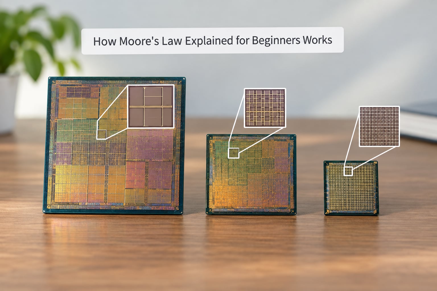
It works as a chain of consequences: make transistors smaller, fit more of them in the same area, get more functions at a lower cost per function, run them without paying proportionally more power, and the chip completes more work per second. Each link depends on the one before it, and the slowest link has always been the one to watch.
Step one: the transistor gets smaller
A transistor is a voltage-controlled switch. A voltage on its gate terminal either allows current to flow between source and drain or blocks it, and that binary on or off state is the physical basis of every bit a computer processes. Shrinking the switch means it takes up less area on the die, leaks less current while idle, and can be switched faster.
Step two: density rises
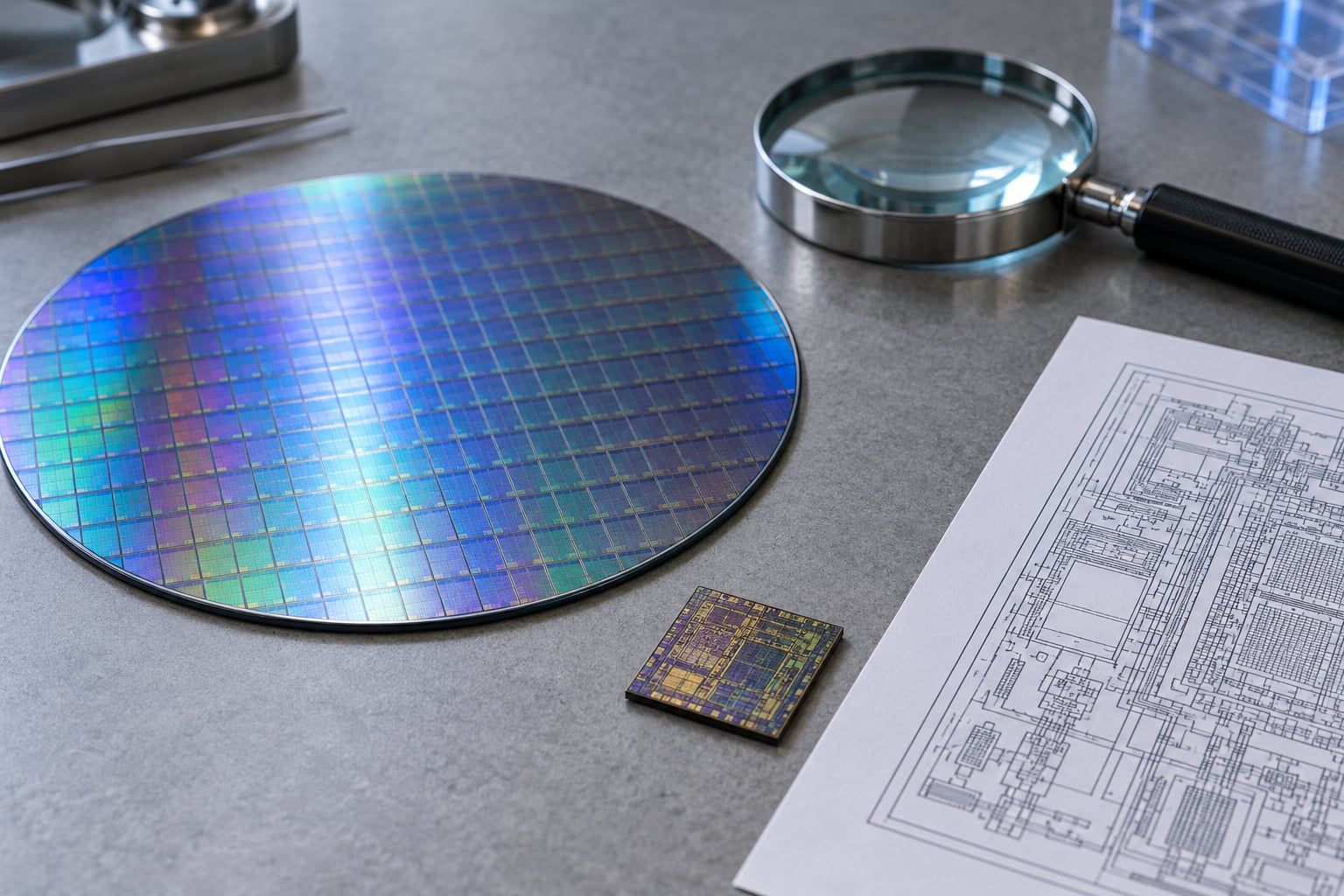
Density is transistors per unit area, and it is the quantity the law actually names. Fitting more switches into the same footprint means shorter distances for signals to travel, and shorter signal paths are what allow a chip to be clocked faster without becoming unusable.
Step three: cost per function falls
Here is the part that changed the world, and it is not a speed story at all. A modern wafer carries a large population of identical dies, and a small defect anywhere on that wafer can spoil the whole sheet. As designs shrank, the yield of good dies per wafer rose steeply, and industry practice moved toward a yield model in which cost per die falls even as the die itself grows. The result was that the price of a given function, whether a logic operation or a bit of memory, fell by orders of magnitude across the industry’s history.
Step four: more work per second, not just more transistors
Transistor count and processor speed are related but not identical, and conflating them causes most beginner confusion. More transistors can be arranged as more arithmetic units running in parallel, more on-chip memory to reduce slow trips to main memory, more cache, or dedicated blocks for particular jobs. A chip with twice the transistors of its predecessor may be only modestly faster, if the extra transistors were spent on features that do not help the workload you care about. What reliably improves is performance per watt, because the same task finishes using less energy and generating less heat.
Why Do Chipmakers Want More Transistors?
Chipmakers want more transistors because every additional block of silicon is room for another job, and because moving work on-chip is far cheaper than moving it off-chip. The historical record shows what those extra jobs were.
| Chip and year | Transistor count | What the extra transistors bought |
|---|---|---|
| Intel 4004, 1971 | about 2,300 | A commercial general-purpose processor on a single chip, replacing several parts |
| Intel 8086, 1978 | about 29,000 | A 16-bit architecture and address space large enough for real software |
| Pentium, 1993 | about 3.1 million | Dual pipelines, on-chip cache and floating-point hardware |
| Pentium 4, 2000 | about 42 million | Deep speculative execution pipelines and large secondary caches |
| Core 2 Duo, 2006 | about 291 million | Two complete cores plus substantially larger shared cache on one die |
| Leading-edge AI accelerators, 2020s | tens of billions | Hundreds of thousands of matrix-multiply elements, plus large bandwidth memory interfaces |
Read that table as a list of answers to the same question: what is the extra silicon for? Early chips used it to become general-purpose at all. Then to widen registers and memory addressing. Then for pipelining and floating-point maths. Then for multiple cores. Then, in accelerators, for a very large number of simple identical compute elements that do one job extraordinarily well.
That last shift explains the economics. When a chip spends most of its transistors on repetitive arithmetic, adding more of them scales throughput almost linearly, which is why AI hardware has outpaced the old pattern of general-purpose performance gains.
What Does Moore’s Law Not Say?
Moore’s Law does not say that every computer gets twice as fast every two years, and it does not say that all technology doubles. It is an observation about one quantity, the number of transistors on a chip, and most confident misuse comes from expanding it beyond that scope.
It is not a statement about processor speed
Clock speed, instructions per clock, memory bandwidth and software efficiency all matter to how fast a machine feels. Two chips with similar transistor counts can perform very differently, and two generations of the same product line can differ in speed by a few percent while the transistor count doubles.
It is not a law of physics
Nothing in the equations of electromagnetism requires transistor density to double on any schedule. The trend persisted because the industry treated it as a shared engineering target and funded decades of research to hit it. When a target stops being economical, the target changes.
Is Moore’s Law 18 months or 24 months?
Both numbers trace to real sources, and this is the single most common point of confusion. Moore’s 1965 article referred to doubling roughly every year. His 1975 revision changed that to approximately every two years, and that figure is the one in his name. The 18-month number came from a different exercise: in the mid-1970s the industry worked back through successive generations of its own roadmaps and settled on a cadence of about four generations every three years, roughly 18 months between process generations, as a rule of thumb for scheduling product cycles. So 24 months is Moore’s number, and 18 months is an industry planning convention.
It never covered everything
Battery chemistry, display technology, memory capacity, storage density and network bandwidth have each followed their own curves, sometimes faster and sometimes slower. Moore’s Law describes the density of transistors, not the pace of progress in every field engineers happen to be improving.
How Has Moore’s Law Changed Since 1965?
The law has survived by being restated whenever the old mechanism stopped working. The doubling rate held, but the way chipmakers achieved it has been rewritten several times.
Planar scaling and the shrinking of every dimension
For roughly three decades the approach was geometric: shrink the gate length, shrink the channel, shrink the metal interconnect, and pack the resulting cells more tightly. Each generation reduced several dimensions at once, and the transistor count of a flagship part rose from a few thousand in 1971 to tens of millions by 2000.
Copper, low-k dielectrics and taller structures
Simple lateral shrinking eventually hit interconnect problems, since resistance and signal delay in the wiring started to dominate. Adding copper conductors and lower-permittivity insulating materials pulled the wiring back into proportion, and building taller cells allowed the same footprint to hold more.
FinFET and gate-all-around transistors
Planar transistors leaked too much current once the channel became short, which wasted power and generated heat that had nowhere to go. The industry’s answer in the early 2010s was the FinFET, a three-dimensional channel that gives the gate better control over the current path. The current generation of that idea, the gate-all-around transistor, wraps the gate on all four sides, and it is what allows the smallest nodes of the 2020s to keep their power characteristics in check.
EUV lithography and three-dimensional stacking
Printers using extreme ultraviolet light at shorter wavelengths made smaller feature sizes printable at all, and stacking layers of transistors and interconnect vertically is now a routine way to add capacity that lateral shrinking can no longer deliver.
Moore’s own later framing
Moore revised the statement several times, saying in the 1970s that the doubling of complexity was the meaningful part, and remarking later that the trend could not continue indefinitely. He lived to see his name attached to a phrase that outlived the mechanism he originally described.
Why Has Progress Slowed Down?
Progress has slowed because the cheap problems were solved first. Each remaining barrier is physical, financial or practical, and the industry now attacks several at once.
Leakage and heat
A transistor in its off state should block current completely. As channels shorten, the barrier that blocks them thins, and current leaks across even when the switch is off. More power is wasted at idle, and more heat must be removed, which caps how often the whole chip can be clocked.
Power density has stopped falling
For most of the industry’s history, chip power and clock speed were flat or falling, which let every generation run faster. That stopped decades ago, so gains now have to come from architecture, efficiency and specialisation rather than from raw frequency.
Manufacturing cost and complexity
Each generation requires new process equipment, new mask sets and longer cycles, and the cost of a leading-edge fabrication plant rises with every node. At some point the projected revenue from a smaller transistor does not cover the cost of building the line that makes it, and the economically useful node stops advancing.
Interconnect delay
Signals crossing a die on metal wires do not travel at the speed of electrons in a vacuum. As transistors became tiny, the wires connecting them became the bottleneck, and the industry has been forced to add repeaters, specialised caches and system-level interconnect rather than relying on shrink alone.
Physical and supply limits
At the smallest feature sizes, materials stop behaving predictably, individual transistors vary widely, and the masks required to print them approach dimensions that strain the patterning equipment. The easy geometry of a uniform rectangular channel also gave way to three-dimensional structures that are far harder to manufacture consistently.
What Replaces Simple Transistor Shrinking?
Nothing replaces Moore’s Law all at once. The current answer is a bundle of techniques, each contributing a part of the improvement that shrink used to provide alone.
Chiplets and advanced packaging
Instead of building one enormous die, engineers cut a design into smaller dies, called chiplets, and connect them on a shared package. Yield improves because a defect affects a smaller area, and different blocks can be built on whichever process suits them best. Large cache and large accelerator arrays, which would be uneconomical as part of a single monolithic die, become practical this way. There is a widely repeated argument among hardware builders that Moore’s Law is over when you apply it to a single piece of silicon, and still running when you apply it to a chiplet package.
Two and three-dimensional integration
Stacking dies and memory directly above a processor cuts the distance data must travel, which is one of the main limits on modern system performance. The bandwidth gain is often larger than what lateral shrink provides at the same node.
Specialised accelerators
Graphics processors, tensor processors, encryption engines and inference chips use a large share of their transistors for one family of operations, and they scale almost linearly when you add more. That is a different route to more work per chip than the general-purpose pipeline improvements of the past.
New transistor architectures
Gate-all-around transistors, stacked nanosheet channels and carbon-based channels in research all aim to restore electrostatic control that planar shrink lost. They extend the life of shrink rather than replace it.
System-level and algorithmic gains
Data centres now recover much of their performance growth from better scheduling, memory architecture, compression and specialised hardware that previously ran on general-purpose processors. The work moved from the transistor to the system, which is a harder engineering problem and a less satisfying one to describe as a law.
What Does Moore’s Law Mean for Beginners Using Technology?
It means the trend that put a computer in your pocket, let it run for a day on one charge, and made large-scale services cheap enough to use every day. Its effects show up in five places, and they are worth separating because they follow different curves.
Processor performance
Your phone and laptop contain the same class of logic that filled a room in the 1970s. Performance gains since then have come from a mixture of shrink, multicore design, faster memory and better software, and no single one of those alone explains a modern computer’s capability.
Battery life
Battery life improved because chips became far more efficient per task, not because batteries became dramatically better. Display technology and software play a large role as well, which is why efficiency gains do not translate directly into a doubling of runtime.
Storage, memory and networking
Storage density and memory capacity followed their own trajectories, but each benefited from lower cost per transistor in the logic that manages them. Wireless standards and fibre advanced on separate schedules, which is why a phone can have excellent connectivity built on a network that is decades old.
Software responsiveness
Applications feel faster when chips have more cores, more cache and dedicated accelerators, but a badly written program will stay badly written at any transistor count. This is the practical reason the law is not a promise about your experience using a device.
Cars, machines and AI
Modern vehicles run substantial compute for driver assistance, and industrial equipment uses dense logic for sensing and control. AI is the loudest current example: training and running large models depends on accelerators whose throughput has grown faster than the general-purpose trend, and on memory bandwidth delivered by advanced packaging. Whether that counts as Moore’s Law continuing is a genuine argument, and sensible people disagree. The transistors are still obeying a doubling rhythm; what has changed is the amount of useful work each transistor is asked to do.
Frequently Asked Questions
Can you explain Moore’s Law in a simple way?
A transistor is a tiny electronic switch, and a chip is a large number of them wired together. Moore noticed that chip makers were able to double the number of switches on a chip roughly every two years. More switches means more room for calculation, memory and specialised blocks, so a chip can do more work for the same cost and energy. That is the whole idea behind the name.
Is Moore’s Law 18 or 24 months?
Both numbers are real, and they come from different sources. Moore’s 1965 article referred to doubling roughly every year, and his 1975 revision changed that to approximately every two years, which is the 24-month figure most people mean today. The 18-month number came from mid-1970s industry roadmaps, where successive process generations were spaced about four generations to every three years as a scheduling rule of thumb.
Is it true that technology doubles every two years?
No. Technology as a whole does not double on any schedule, and neither does your computer. Moore’s Law describes one quantity, the number of transistors on a chip. Some technologies improve faster, some slower, and many change in ways that are not exponential at all. Batteries, displays and wireless standards each follow their own curves, so the familiar claim that everything doubles every two years is a loose summary, not a fact.
Why is Moore’s Law no longer valid?
It is not invalid, but the mechanism has changed. A short transistor channel leaks current, so power and heat rise as features shrink, and those costs eventually exceeded what the extra transistors were worth. Fabrication plants also cost far more at each new node. Engineers responded with three-dimensional transistors, chiplets and advanced packaging, so the density trend continues by a different route than simple lateral shrink.
Is AI faster than Moore’s Law?
That depends on what you measure. AI accelerators have improved throughput faster than general-purpose processors did, because a large share of their transistors perform one repeated operation. System-level gains from better memory and packaging add more. It is fair to say AI compute has outpaced the old performance pattern, but the underlying transistor count still follows a doubling rhythm of its own.
What does Moore’s Law say will happen to microchips over the next ten years?
The historical pattern implies roughly 32 times more transistors in ten years, since the count doubles about five times in that span. The law predicts density, not clock speed, not application speed and not a schedule for any particular product. Real designs have added transistors for cache, accelerators and memory interfaces rather than raw speed, so a 32-fold count increase should be read as a change in what chips contain.
Conclusion: Start With the Core Idea
If you keep one thing from this guide, keep this: more transistors in a given chip area is what makes more computation possible, and everything else follows from that. Moore’s Law is best understood as a sixty-year trend in semiconductor density, not a physical law and not a promise about how fast your devices will feel. Performance depends on clock speed, architecture, memory, cooling and software at the same time. Start there, and the rest of the vocabulary, from process nodes to chiplets, becomes much easier to place.