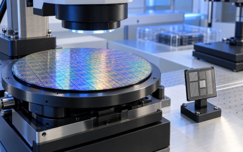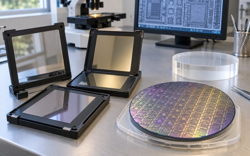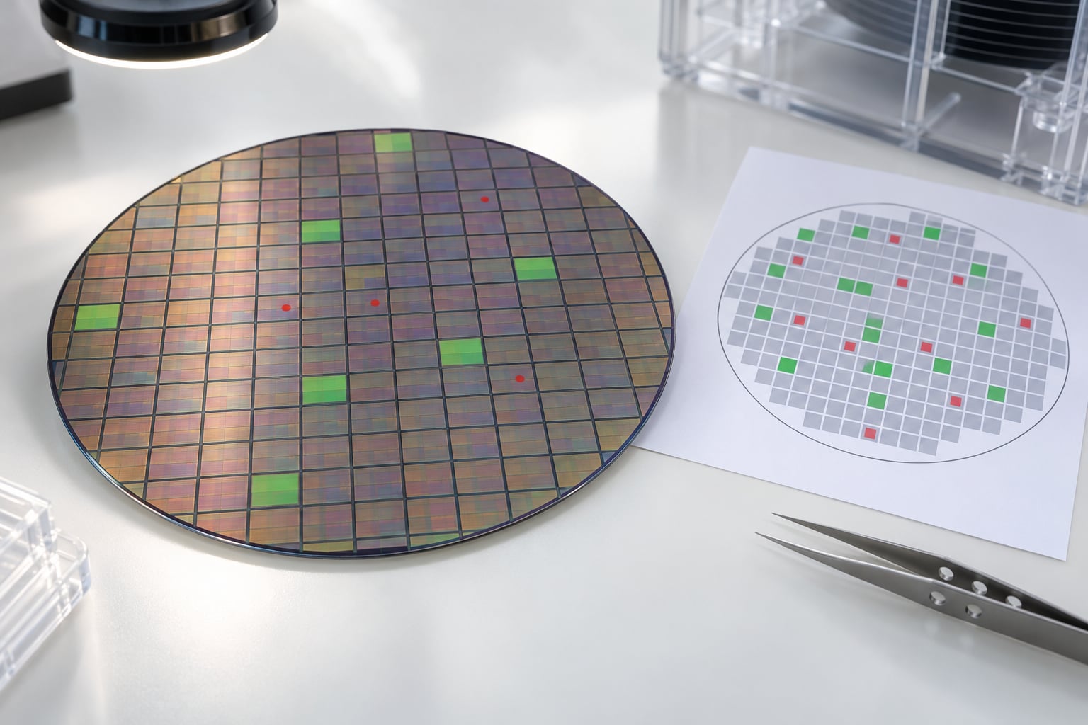
The short version of how semiconductor yield is calculated is one division: the number of functional (good) dies divided by the total number of potential dies on that wafer, multiplied by 100. Everything else in this guide — defect density, statistical models, wafer sort, cost per good die — is a way of getting at those same two numbers.
Below I use the convention that every yield figure quoted is a measured wafer-sort average in high-volume manufacturing, unless I say otherwise. That sounds fussy, but figures for the same node often differ by tens of points depending on whether they came from an early ramp, a single design, or a vendor estimate, and knowing the basis is what makes a number usable.
Table of Contents
- How Semiconductor Yield Is Calculated
- The Inputs Needed for a Yield Calculation
- Yield Formula and Step-by-Step Example
- The four statistical yield models
- How to calculate semiconductor yield in Excel or Google Sheets
- Worked example: from die area to cost per good die
- Why Semiconductor Yield Is Measured at Different Stages
- How Defects and Process Parameters Affect Yield
- How to Interpret a Yield Number
- How to Improve Semiconductor Yield Without New Equipment
- Frequently Asked Questions
- What is a good semiconductor yield?
- Is semiconductor yield calculated per wafer or per lot?
- Why can wafer-sort yield differ from final-test yield?
- What is the difference between defect density and die yield?
- Can semiconductor yield reach 100 percent?
- How do foundries use yield data to estimate chip cost?
- Key Takeaways
How Semiconductor Yield Is Calculated
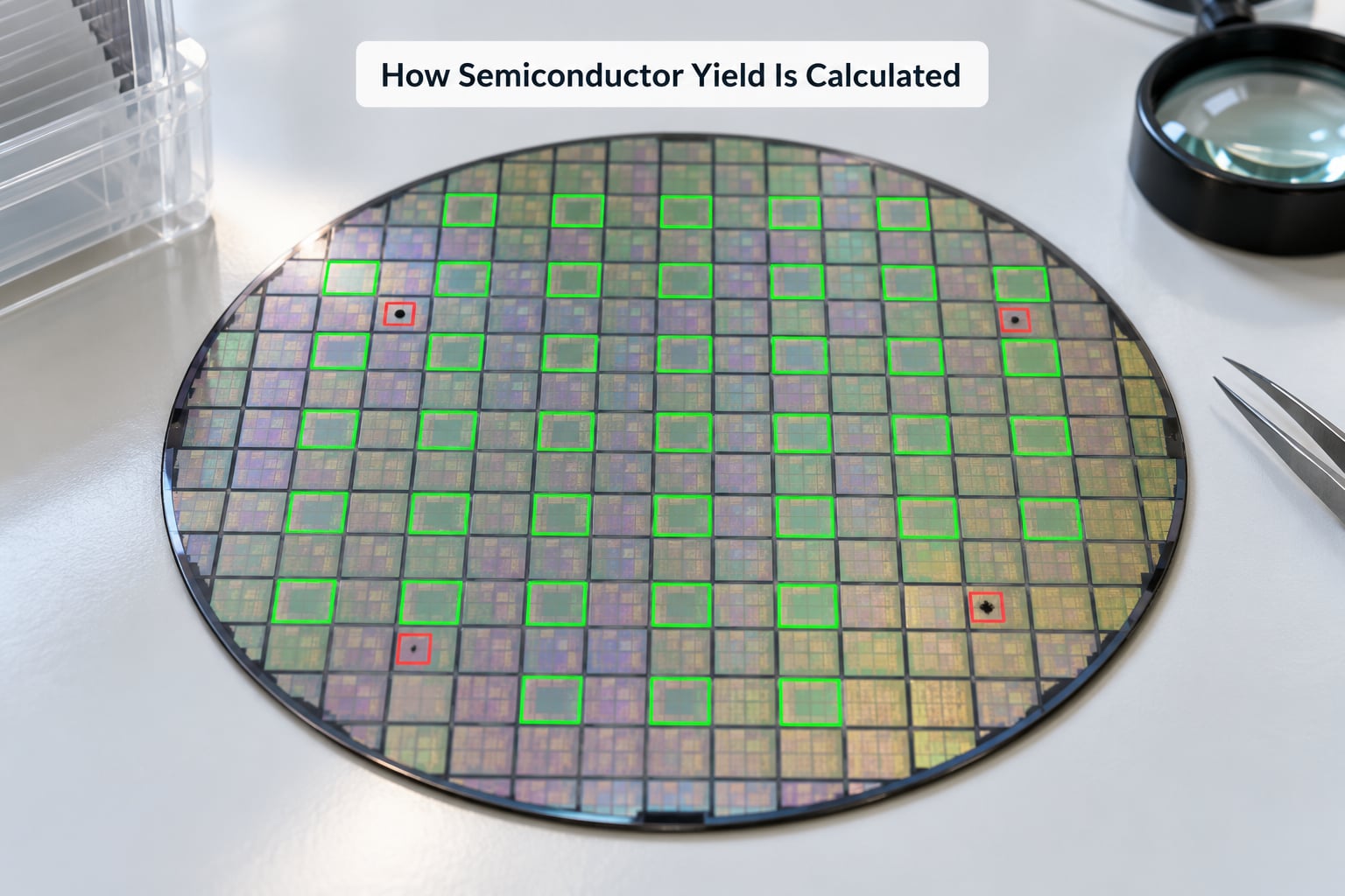
Yield (%) = (Functional Dies / Potential Dies) x 100
The numerator is the count of dies that passed electrical test. The denominator is the gross die count, the number of die positions the wafer layout could physically hold after scribe lines and edge exclusion are removed.
Four different numbers get called “the yield,” and mixing them up causes most of the confusion in press coverage:
- Die yield — good dies divided by gross dies on a single wafer.
- Wafer yield — the same ratio averaged across every wafer in a lot or a run, which is the number most fabs actually track.
- Lot yield — wafers passing final test divided by wafers started, often called the lot pass rate.
- Line yield — the product of per-step yields across every process layer, a rough measure of how repeatable a whole flow is.
As a concrete example: a 300 mm wafer laid out for 1335 gross dies comes back from wafer sort with 1288 passing dies. Die yield is 1288 / 1335 = 96.5%. The other 47 dies are scrap, and each one has already absorbed the full cost of the wafer it sat on.
That last point is the reason yield gets so much attention. At a 300 mm wafer with roughly 1300 die positions, dropping from 50% to 70% yield cuts the cost carried by each good die by about 29%, because the same fixed wafer cost gets spread across 40% more working chips.
The Inputs Needed for a Yield Calculation
Six inputs go into any real yield report, and the useful thing about naming them is that each one shows up differently in the denominator.
- Wafer starts — wafers released into the flow. This is the denominator for the lot pass rate, not for die yield.
- Gross dies (potential dies) — die positions available, computed from wafer diameter, die area, scribe line width and the exclusion applied at the wafer edge.
- Good dies — dies passing the pass/fail criteria at a given test stage.
- Defecting dies — dies that failed electrical test, plus dies scrapped before test for handling damage or process abort.
- Test exclusions — die positions deliberately not probed: known probe-mark failures, scribe-line bridges, edge dice marked by the scribe map, or positions excluded because the customer did not order that bin.
- Inspection and test data — inline defect maps from metrology tools, parametric wafer test results, and the pass/fail wafer map from the probe station.
The denominator choice matters more than people expect. If you divide good dies by gross dies, edge and scribe exclusions quietly inflate the result. If you divide by probed dies, you get the honest process signal but no longer match the wafer cost you are trying to justify.
Most production reporting systems therefore publish both: a gross-die yield for cost and capacity work, and a probed-die yield for process monitoring. Know which one you are quoting.
Yield Formula and Step-by-Step Example
The simple ratio above tells you what happened on one wafer. To predict what will happen, foundries model it from defect density, the number of random defects per square centimetre, usually written D0.
The four statistical yield models
Every model reduces to one quantity: the expected number of defects landing on a die, written as A x D0, where A is die area in cm2.
- Poisson — Y = e^(-A x D0). Assumes defects hit randomly and independently, with no clustering and no die having a defect susceptibility. Best for small dies on mature processes.
- Murphy — Y = ((1 – e^(-A x D0)) / (A x D0))^2. Assumes each die has two sensitive regions, so two chances to be hit. Closer to reality for medium and large dies.
- Seeds — Y = e^(-sqrt(A x D0)). Assumes defects cluster, so extra area adds less risk than a Poisson model predicts. Useful when defect maps show clusters.
- Bose-Einstein — Y = 1 / (1 + A x D0)^n. Multiplies the effect across n critical layers, which is how yield is often estimated for a full logic process.
| Model | Formula | Core assumption | Use it when |
|---|---|---|---|
| Poisson | Y = e^(-A x D0) | Random, independent defects | Small dies, mature nodes |
| Murphy | Y = ((1 – e^(-A x D0)) / (A x D0))^2 | Two sensitive regions per die | Medium and large dies |
| Seeds | Y = e^(-sqrt(A x D0)) | Defects cluster | Clustered inline defect maps |
| Bose-Einstein | Y = 1 / (1 + A x D0)^n | n critical layers each add risk | Estimating line yield by layer count |
| Negative Binomial | Poisson with cluster parameter alpha | Clustering with a fitted alpha | Alpha known from defect maps |
Here is what those models produce across a realistic range of defect densities. The two die areas matter: the same fab, the same day, very different numbers.
| D0 (defects/cm2) | Poisson, 0.45 cm2 die | Murphy, 0.45 cm2 die | Poisson, 8 cm2 die | Murphy, 8 cm2 die | Seeds, 8 cm2 die |
|---|---|---|---|---|---|
| 0.01 | 99.6% | 99.6% | 92.3% | 92.4% | 75.4% |
| 0.05 | 97.8% | 97.8% | 67.0% | 68.0% | 53.2% |
| 0.10 | 95.6% | 95.6% | 44.9% | 47.4% | 40.9% |
| 0.20 | 91.4% | 91.7% | 20.2% | 24.9% | 28.2% |
| 0.40 | 83.5% | 83.7% | 4.1% | 9.0% | 16.7% |
| 1.00 | 63.8% | 64.9% | 0.03% | 1.6% | 5.9% |
The gap between the two die areas at the same D0 is the whole reason smaller dies yield better. Poisson and Murphy agree almost exactly below about 0.5 cm2, which is why the simple model gets away with being wrong for a while.
How to calculate semiconductor yield in Excel or Google Sheets
For a live number from a wafer map rather than a model estimate, you only need three columns: die location, pass/fail, and exclusion flag.
Column A holds the die ID. Column B holds the wafer sort result — 1 for pass, 0 for fail. Column C holds 1 where the die was excluded and 0 where it was probed.
=COUNTIFS(B2:B5000,1,C2:C5000,0) / (COUNTIF(B2:B5000,">=0") - COUNTIFS(C2:C5000,1))
That numerator counts passing, non-excluded dies; the denominator counts every die position minus the excluded ones. Format the cell as a percentage. For a yield-versus-defect-density sweep, put D0 values down column A and Poisson results beside them:
=EXP(-($A2*$B$1))where B1 holds die area in cm2. Wrap it in a data table and you get the curve in seconds.
Worked example: from die area to cost per good die
Take a 45 mm2 die on a 300 mm wafer. That is 0.45 cm2, which is where the unit trap sits — if you feed 45 into a model expecting cm2 you will get nonsense.
Step 1, gross dies. N_die = floor(pi x (D_w/2)^2 x u / A), with u about 0.85 for edge and scribe exclusion. 300 mm gives roughly 1335 die positions for this die.
Step 2, yield. Poisson with D0 = 0.08 gives A x D0 = 0.036 and Y = e^-0.036 = 96.5%. Murphy gives 96.5% too, which is a useful sanity check at this die size.
Step 3, good dies. 1335 x 0.965 gives about 1288 working dies per wafer.
Step 4, cost per good die. Cost per good die equals wafer cost divided by good dies. At 96.5% yield, each good die carries about 0.78% of the wafer cost. At 50% yield the same wafer yields about 668 good dies, so each one carries 1.5% — nearly twice as much. At 5% yield, roughly 67 good dies, each carrying about 15% of a wafer’s cost.
Now put the same 300 mm wafer behind an 800 mm2 die at the same D0 of 0.08. A x D0 becomes 0.64, so Poisson falls to about 53% and Murphy to about 55%. The position count matters just as much: roughly 75 gross dies per wafer, so about 40 good dies. The small die delivers more than 30 times as many working chips from the identical wafer.
Why Semiconductor Yield Is Measured at Different Stages
Every yield number is tied to a test stage, and the stages disagree because each one applies a different definition of working.
Provisional yield is a working estimate before wafer sort finishes, built from partial wafer maps or inline defect counts. Treat it as directional.
Parametric wafer test runs before probing and checks process parameters — leakage, threshold voltage, resistance — across selected structures. It flags a drifting tool long before die yield visibly moves.
Wafer sort is the main event. A probe station lands on every die, runs functional verification, and writes a pass/fail bin per die into a wafer map. This is the number usually meant by “the yield.”
Final test happens after dicing and packaging, and it always comes in a bit below wafer sort. The die passed before it was cut out of the wafer, and between those two moments it absorbs handling, package stress, and bonding damage.
Field yield is what customers actually experience. It sits below final test, and the gap is dominated by latent defects — weak spots that passed a room-temperature test and failed later under heat or voltage.
There is also the yield loss between wafer sort and final test, which is measured directly by comparing the two records for the same die IDs. It is one of the cleanest process health indicators a fab has.
How Defects and Process Parameters Affect Yield
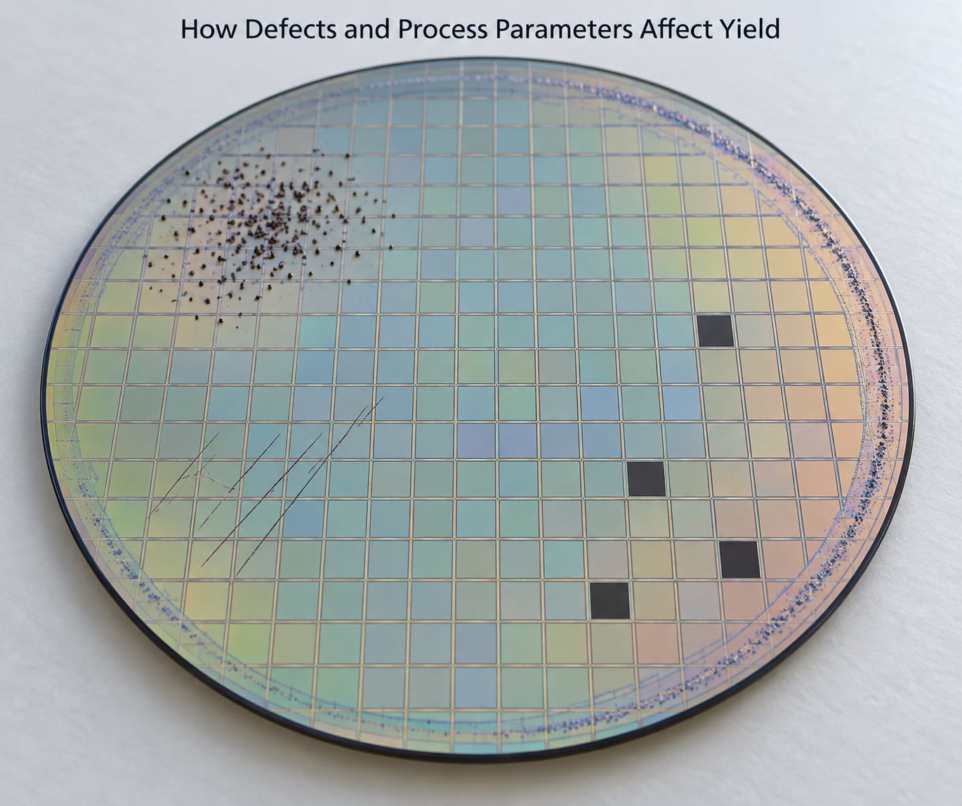
Defect density is a summary, not a diagnosis. The shape of the defect map tells you which mechanism is actually costing you dies.
- Random particles scatter evenly and are what the Poisson model assumes. Airborne contamination, residual resist flakes.
- Edge rings follow the wafer edge and come from plating uniformity, edge exclusion settings and resist coating behaviour near the chuck.
- Scratches and handling marks trace back to robot trajectories, FOUP transfer and wafer shipping, and usually look like arcs or straight lines rather than points.
- Clusters are particle showers from a single burst event. They break Poisson badly and are why the Seeds and Negative Binomial models exist.
- Systematic patterns — repeating lines or arrays tied to reticle coordinates — point at a mask or stepper problem, not contamination.
A killer defect is the one that lands on a circuit element and takes out a whole function: a bridge across a line, a cut in a via, a particle over an active region. As nodes shrink, the critical dimension falls and the killer defect shrinks with it, roughly to about a third of the design rule, which means the same physical particle becomes lethal.
Process excursions show up the same way. A drifted etch bias, a hot bath, an out-of-spec gas flow, or a lamp ageing in a scanner will each produce a yield loss that is specific to the layer involved, and the wafer map signature — radial, linear, or quadrant-shaped — usually identifies which.
Node size makes this harder because critical layers multiply. If each of 70 critical layers carries 99% yield, line yield is 0.99^70, about 49%. That is why an advanced process with excellent defect density can still show modest line yield, and why chiplet designs keep winning on economics: each die gets fewer critical layers over a smaller area.
How to Interpret a Yield Number
Start with the denominator, then the stage, then the basis. A yield figure without those three is a number in a vacuum.
Higher yield means each good die carries less of the fixed wafer cost, and because fabrication cost per wafer keeps climbing at advanced nodes, that effect compounds. The relationship is not linear: cost per good die falls as the reciprocal of yield, so the improvement from 50% to 60% is larger than the same jump from 80% to 90%.
Watch four things before you trust a number:
- Sampling. A yield from ten wafers is not a yield from ten thousand. Wafer-to-wafer spread across a lot is typically a few points, and a small sample can swing the average a lot.
- Product mix. Lots with several mask sets give you a blended number. A big die and a small die in the same lot pull the average in opposite directions.
- Ramp stage. Numbers quoted in the first months of a node are almost always worse than the steady-state value, and improvements are lumpy rather than linear.
- Reporting basis. Vendor-supplied node yield figures are estimates, often extrapolated rather than measured across a full volume population.
Where a figure comes from matters as much as its value. A yield reported by the foundry for its own reference design on a specific customer product at a specific stage is a real measurement. A yield attributed to a node with no design, date or stage named is usually an inference.
How to Improve Semiconductor Yield Without New Equipment
Most yield gains at a mature node come from control, not from capital. Five levers cover the majority of it.
Push on defect detection rather than defect removal. In-line defect inspection from tools such as KLA and Applied Materials only pays off if the data drives action. Automatic defect classification that routes escapees to review keeps inspection at high sensitivity without drowning the review queue.
Tighten process windows on the layers that cost the most. Not every layer deserves equal effort. Target the two or three layers whose loss dominates the wafer map, and spend your SPC limits there.
Have an excursion response plan before you need one. Decide, in advance, which readings trigger a hold, who authorises the restart, and how many wafers get reworked or scrapped. Ad-hoc decisions here are expensive.
Run statistical process control on parameters that lead yield, not ones that trail it. Chamber pressure, gas flow, track bake temperature and developer concentration move yield days before the wafer map shows it.
Do root-cause analysis at the die, not the tool. When a lot drops, correlate failing die coordinates against defect maps and equipment history. The signature usually names the mechanism faster than a process FMEA does.
Design choices matter too, and they are free. Smaller die area raises yield at any defect density. Chiplets convert one large yield gamble into several small independent ones. Redundancy — spare rows, repairable fuses, redundant periphery — turns a scrap die into a lower-bin die rather than a loss. Design-for-manufacturability rules that keep dense structures away from wafer edges cut the edge-ring loss directly.
Frequently Asked Questions
What is a good semiconductor yield?
There is no single good number, because yield depends on die area, defect density and process maturity. On a mature node with die areas under 0.5 cm2, high-volume wafers routinely run above 90%. Large dies on newer nodes can look healthy at 60% while a small die on the same lot reads 97%. Judge a yield against what the process has historically produced at that die size, not against a universal threshold.
Is semiconductor yield calculated per wafer or per lot?
Both, for different purposes. Die yield and wafer yield are calculated per wafer, dividing good dies by gross or probed dies. Lot yield, often called the lot pass rate, divides wafers passing final test by wafers started. Capacity and cost planning use wafer yield; process monitoring and lot disposition use lot yield.
Why can wafer-sort yield differ from final-test yield?
The die is handled, diced, packaged and electrically retested between those two points. Mechanical stress from dicing and packaging, bond damage, and marginal parts that only fail under test conditions all remove dies that passed at wafer sort. A typical gap of a few percentage points is normal; a much larger one usually signals handling or packaging problems rather than front-end defects.
What is the difference between defect density and die yield?
Defect density D0 is an input measured in defects per square centimetre, usually from inline inspection. Die yield is the output expressed as a percentage of good dies. Yield is a function of defect density, die area, clustering and the model chosen, so the same defect density gives very different yield for a 0.45 cm2 die and an 8 cm2 die.
Can semiconductor yield reach 100 percent?
Not on a wafer carrying hundreds of die positions. With any non-zero defect density, Poisson mathematics predicts a non-zero probability of at least one hit per wafer, and real fabs also scrap edge and scribe exclusions. Small die counts on a large die can get very close, which is why foundries like it, but a full wafer at a mature node tops out in the high 90s rather than at 100.
How do foundries use yield data to estimate chip cost?
They divide wafer cost by good dies per wafer, where good dies equals gross dies times predicted yield for the given die area and defect density. Because cost per good die is the reciprocal of yield, early improvements move the number a lot: moving from 50% to 70% yield cuts cost per die by about 29% with no change in wafer cost. Chiplet economics run on the same arithmetic applied per die.
Key Takeaways
Good dies divided by gross dies, at a named test stage. That is the whole of how semiconductor yield is calculated, and everything else in this guide is a refinement of it. Start with the numbers you can verify: gross dies on the wafer, good dies out of wafer sort, and the stage both were measured at.
Two habits keep the rest honest. Convert units before you compute anything, since the millimetre-to-centimetre error is the single most common mistake in yield spreadsheets. And state the basis whenever you quote a figure — stage, ramp timing, design and sample size — because an uncontextualised percentage is the least useful number in the industry.