Flip chip packaging is a way of connecting a bare semiconductor die to a substrate or circuit board: the die is turned face-down so its interconnect bumps sit directly on the board pads. That short, direct connection buys you higher pin counts, lower inductance, a smaller package, and a cleaner thermal path than the wire bonds it replaces.
Most people meet the term in a datasheet long before they ever see a package. Once you know what the bumps are doing, though, the rest is fairly mechanical: bump the wafer, cut the die, flip it, place it, reflow it, fill the gap. Here is how that works, what it costs you, and where it beats the older alternatives.
Table of Contents
- What Is Flip Chip Packaging?
- The four building blocks
- How Does Flip Chip Packaging Work?
- How the interconnect layers stack up
- What Are the Main Flip Chip Technologies?
- How Is a Flip Chip Package Manufactured and Assembled?
- What Are the Benefits of Flip Chip Packaging?
- Benefits that follow from the connection method
- Benefits that depend on design and materials
- What Are the Disadvantages and Design Challenges?
- What goes wrong, and how you catch it
- When Is Flip Chip Packaging Used?
- Flip Chip Packaging vs Wire Bonding: What Changes?
- Frequently Asked Questions
- What is the flip chip packaging process?
- How does a flip chip work?
- What are the main downsides of flip chip technology?
- Is underfill always required for flip chip?
- Can a flip chip assembly be reworked?
- What is the difference between flip chip and wafer-level packaging?
- Conclusion
What Is Flip Chip Packaging?
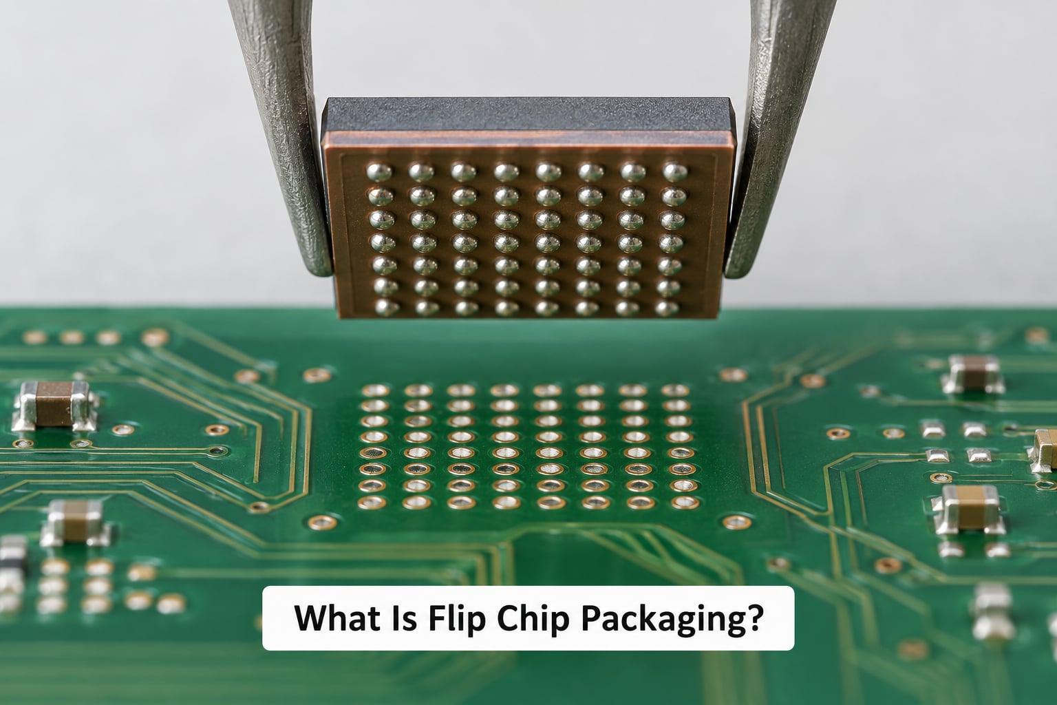
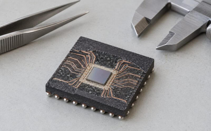
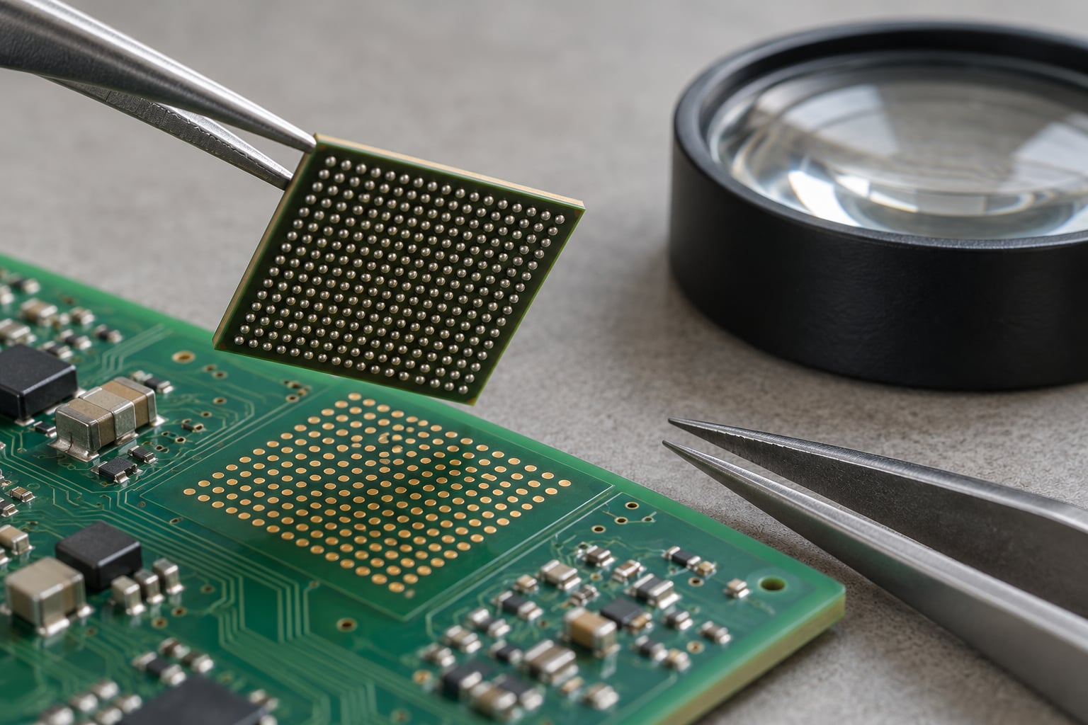
Flip chip packaging is a semiconductor assembly technique in which a bare die is flipped face-down and bonded directly to a substrate or printed circuit board through an array of solder bumps, gold studs, or copper pillars. It replaces the perimeter wire bonds used in older packages and gives higher I/O density, shorter electrical paths, lower inductance, and a smaller profile.
Every flip chip assembly is the same four ingredients. Understanding them separately makes the whole subject much easier.
The four building blocks
- The die. A bare, unpackaged piece of silicon. A flip chip can be a full ASIC, a memory die, or a tiny IoT sensor; it does not have to be large or expensive.
- The interconnect bumps. Solder balls, copper pillars with solder caps, or gold studs formed on the die’s bond pads during wafer bumping. This is the part that actually touches the board.
- The under bump metallization, or UBM. A thin stack of titanium, nickel, vanadium and copper under each bump that gives solder something to wet and gives the pad a reliable solder mask opening.
- The substrate. The organic package substrate or the bare PCB that receives the die. Many designs stop here; others add solder balls on the package underside and mount the package to the board as a second step.
What makes it a flip chip rather than a wire bond is simply where the connection lands. Wire bonding can only reach the metal ring around the edge of a die. A flip chip connects across the entire die surface, which is why the technique is called an area array.
That boundary is also why the word causes confusion. A die bumped and bonded straight onto a board is a flip chip. A die bumped at wafer level, given a redistribution layer, then packaged is wafer-level packaging. Fan-out packaging moves the die onto a moulded carrier and reroutes from there. Flip chip is a connection method; those are architectures built on top of it.
How Does Flip Chip Packaging Work?
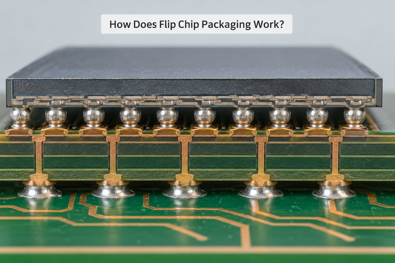
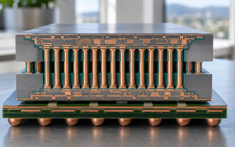
A signal moves through a flip chip in one straight line. It leaves the transistor through a metal layer to a bond pad, drops into the UBM, passes up through the solder bump, lands on a substrate pad, goes through a via into an internal plane or another trace, and finally out to a board trace. There is no wire arc in that path anywhere.
Because the path is short and mostly vertical, its parasitic inductance is tiny. Industry figures put a flip chip interconnect under 0.1 nH, against the 1-3 nH you get from a typical wire loop of 1-3 mm. On a multi-gigabit link that is the difference between a design that closes and one that does not.
How the interconnect layers stack up
From the silicon outward, the stack usually reads: bond pad metal, UBM, the solder bump itself, a matching land on the substrate, an organic substrate or board dielectric, and finally the ground and power planes. The bump pitch, typically 0.4-0.5 mm in mainstream production, sets how many of those vertical connections fit in a given area.
Reflow does the actual joining. Flux residue wets the solder, the package is heated through a controlled profile peaking around 245-260 degrees C, and surface tension pulls each bump onto its land. That self-alignment is why flip chip assembly tolerates placement variation of roughly +/-15-50 um and still yields a working joint. The bumps find their own centre, so the placement machine does not have to be perfect.
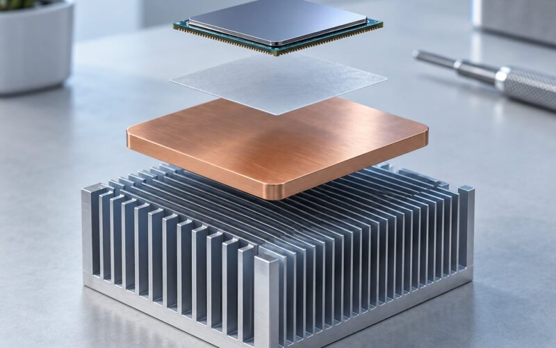
Heat then has somewhere to go. The die sits directly on the board, so the bumps, the substrate and a thermal interface compound form a direct path to the board rather than routing through a wire bond. That is a genuine advantage, and it is also why a thermal problem in a flip chip still ends up a board problem.
Underfill handles the rest. A resin is dispensed around the die, drawn into the gap by capillary action, and cured. It glues the die to the substrate, spreads the thermomechanical stress across thousands of connections instead of concentrating it at the corners, and locks the assembly against the shear that temperature cycling would otherwise produce. The trade is repairability: once that resin is cured, the joint is not serviceable.
What Are the Main Flip Chip Technologies?
The interconnect technology is the biggest single decision after the die. Solder bumps remain the volume default, but each option trades standoff height, pitch, process complexity and cost differently.
| Technology | Typical pitch | Standoff height | Where it fits |
|---|---|---|---|
| C4 high-lead solder | Coarse, roughly 100-250 um | High, around 200 um and above | Legacy plastic packages, thermal-pad connections, older ceramic work |
| Eutectic tin-lead | Fine relative to C4 | Low, roughly 50-100 um | High-density work where the assembly still runs on a leaded profile; largely phased out of new consumer designs |
| Lead-free SAC-type solder | 0.4-0.5 mm mainstream | 200-300 um | The volume standard for RoHS-compliant production across mobile, networking and automotive |
| Copper pillar with solder cap | Fine, roughly 100-200 um | Fixed by pillar height, 50-150 um | Fine-pitch and low-profile parts, computer packages where Z-height is critical |
| Gold stud, thermosonic | Very fine, below 100 um | 20-50 um | Mems, optoelectronics, high-frequency RF and microwave devices |
| Thermocompression or hybrid bonding | Sub-10 um in research and leading parts | Near zero | 3D stacking and chiplets where copper-to-copper contact replaces solder entirely |
Two honest notes on that table. These are typical bands, not design rules; exact limits move with alloy, geometry and equipment, and I would treat any figure quoted in an older article as a starting point rather than a specification.
The second note is about the fine-pitch barrier. Volume flip chip does not scale easily below about 150 um bump pitch without exotic cost, which is exactly the frustration practitioners raise when they need 40 um. When the pitch demands goes past that wall, the usual answer is not a smaller bump. It is a redistribution layer routing connections out to a coarser pitch, or moving to hybrid bonding.
How Is a Flip Chip Package Manufactured and Assembled?
The process below describes the common solder-bump flow. Thermocompression and hybrid bonding add a bond step in place of reflow, but the order of operations is broadly the same.
- Wafer preparation. The wafer arrives with a patterned pad stack. It is cleaned, thermally treated, and inspected so that every die starts from a known surface condition.
- UBM formation. A seed layer is deposited and patterned, then a thicker metal layer is plated to create the under bump metallization on each pad. This is the layer that later solder wets to.
- Bumping. Solder is deposited by stencil printing and reflowed, or plated onto the wafer. Copper pillars are plated first and the solder cap is added afterward; gold studs are deposited by wire bonding equipment and then flattened.
- RDL, where required. For wafer-level and fan-out parts, a redistribution layer is built in dielectric and thin metal to fan the fine-pitch bumps out to a coarser landing grid.
- Wafer test and known good die. Each die is probed while still on the wafer, so a known good die can be sorted before any money is spent packaging it. This is the single biggest yield lever in the whole flow.
- Dicing. The wafer is cut into individual die. Thin wafers and low-kernel-loss blades matter here; a cracked die is a scrapped die.
- Placement with flux. A stencil deposits no-clean or tacky flux, and the placement machine picks the die, rotates it 180 degrees, and sets it down bumped side onto the board or substrate. Vision or a known-good-die record guides the alignment.
- Reflow. The assembly goes through a controlled thermal profile that brings the solder to a peak in the 245-260 degree C region and holds it there long enough for the intermetallic compound to form, then cools on a controlled ramp. Ramp rate matters as much as peak temperature.
- Underfill and cure. Epoxy is dispensed beside the die and drawn under it, or the part is pre-filled before placement with a no-flow material. The assembly is then heated to cure the resin.
- Inspection and test. X-ray looks for voids, bridging and missing joints; scanning acoustic microscopy looks for delamination and underfill voids. Then it goes to final test.
Order can differ, and it does. Some manufacturers apply underfill before placement, some mould it after reflow, and some apply it at wafer level to keep reflow off the sensitive material entirely. Each rearrangement trades throughput against process risk.
What Are the Benefits of Flip Chip Packaging?
Some of the benefits of flip chip packaging are structural and follow directly from the connection method. Others depend on getting the package, substrate and board right, and it is worth keeping the two lists apart.
Benefits that follow from the connection method
- Higher I/O density. The whole die surface is available, not just the perimeter, which is what makes large ball-count packages possible.
- Short electrical paths. On the order of 50-100 um instead of a 1-3 mm wire loop.
- Lower parasitic inductance. Typically under 0.1 nH per interconnect. This directly limits power-delivery-network impedance and noise, which matters when Vnoise scales with transient current times network impedance.
- Lower profile and smaller area. No loop height to accommodate, and no bond pad ring to leave empty around the die edge.
- Fewer process steps. One placement replaces hundreds of wire bonds, and cycle time per part drops sharply at volume.
Benefits that depend on design and materials
- Improved electrical performance at high frequency. Real, but only if the package substrate and PCB escape routing are co-designed with the die. A badly routed escape can throw away everything the interconnect bought.
- A direct thermal path. Real, and also conditional on a thermal interface compound, a heatsink, and a board that can actually move the heat away.
- Better reliability in temperature cycling. Achievable with underfill and a matched build, not automatic. Silicon expands at about 2.6 ppm per degree C while an organic substrate sits around 14-17 ppm per degree C, and that mismatch is the driving stress in the joint.
Not everything marketed under the name holds up. A flip chip on a board with no thermal path will run hotter than a well-cooled wire-bonded design, and no amount of interconnect quality changes that.
What Are the Disadvantages and Design Challenges?
Flip chip is harder to build, harder to inspect, and much harder to fix. Practitioners describe the choice as a trade rather than an upgrade, and the list of costs is real.
- Thermal. The heat path is direct, which helps, but the area available for it is still small and the die may be doing more work per square millimetre than ever before.
- Inspection. Solder joints sit under the die. You cannot look at them with a microscope, so every check is an X-ray, an acoustic scan, or a slice-and-polish sample that destroys the part.
- Rework. An un-underfilled assembly can sometimes be reworked, but cured underfill generally means the part is scrap. Designers rarely price this in early.
- CTE mismatch. The 2.6 versus 14-17 ppm per degree C gap drives cyclic shear at the joint corners every time the board heats and cools.
- Warpage. Large organic packages and thick boards bow during reflow, and a bowed part is a lifted corner, a non-wet joint, or a cracked die.
- Yield and cost. Fine-pitch bumping, wafer-level processing and X-ray coverage are capital-intensive, and each one costs yield somewhere.
- Board and process burden. NSMD or SMD pad choices, surface finish compatibility, stack-up and the reflow profile all have to be designed, not adapted afterwards.
What goes wrong, and how you catch it
| Symptom | Likely cause | How it is found | Prevention |
|---|---|---|---|
| Open circuit on some bumps | Non-wet joint, insufficient flux or too short a reflow soak | Electrical test plus X-ray | Tune the profile, check flux deposit volume, verify pad chemistry |
| Adjacent bumps shorted | Bridging from excess solder or a pad-to-pad spacing error | X-ray | Stencil aperture and thickness control, correct land pattern |
| Intermittent failure after thermal cycling | Solder fatigue from CTE mismatch | Temperature cycling test, cross-section | Underfill, softer pad alloys, strain-relief layout |
| Corner of the die lifts | Package or board warpage during reflow | Scanning acoustic microscopy, X-ray | Warpage control in the substrate stack-up, support during reflow |
| Underfill gaps at the die edge | Voiding from dispense path or cure shrinkage | Scanning acoustic microscopy | Dispense pattern design, filler content, cure ramp |
| Die cracks after bonding | Dicing damage or bonding force on a thin die | Cross-section, dye and pry | Dicing process tuning, lower bond force, stress-relief geometry |
IPC-7094 is the standard most engineers reach for on flip chip and die-size package design and assembly, and J-STD-028 governs the moisture/reflow sensitivity of plastic devices. JEDEC Design Guides 4.7 and 4.18 cover wire bond and flip chip design respectively, and are useful when you need the vocabulary to be exact rather than approximate.
When Is Flip Chip Packaging Used?
Flip chip shows up wherever the I/O count, the data rate, or the physical size leaves no room for a wire loop. The reasons differ by application.
| Application | Why flip chip |
|---|---|
| AI accelerators and HPC ASICs | Thousands of I/O and power bumps, very low inductance for multi-gigabit SerDes links, and a low-inductance power network to keep droop down |
| High bandwidth memory stacks | Dense wide interfaces and very short vertical paths between stacked die and interposer |
| Mobile SoCs and baseband | Area array fits a large pin count into a thin package, which is the whole design goal in a handset |
| RF and mmWave front ends | Short interconnect keeps parasitic inductance low at microwave frequencies, where even a wire loop is a meaningful reactance |
| CMOS image sensors | Very small die mounted directly facing a lens or filter, with the sensor heat path kept off the logic |
| Automotive and industrial parts | Known good die sorting and the reliability of an underfilled area array, where vibration and temperature swings are constant |
| Low-pin-count IoT devices | WLCSP gives the smallest footprint available, at the cost of a harder process to assemble |
| Chiplets and 2.5D/3D integration | Bumping plus redistribution or through-silicon vias is the enabling interconnect; hybrid bonding pushes it further |
The pattern is consistent. Flip chip earns its cost when the connection itself is the bottleneck. A dozen-pin sensor driving a slow interface does not need a 3000-bump array, and forcing one adds cost and process risk for no measurable gain.
Flip Chip Packaging vs Wire Bonding: What Changes?
Wire bonding is cheaper, slower per bond, and far easier to inspect and repair. Flip chip is faster, denser, faster electrically, and much harder to build. Here is the comparison that actually decides it.
| Criterion | Flip chip | Wire bond |
|---|---|---|
| Connection method | Area array of bumps on the die face | Perimeter wires from pad to lead or substrate |
| Signal path length | 50-100 um | 1-3 mm wire loop |
| Interconnect inductance | Under 0.1 nH | 1-3 nH |
| I/O density | Set by bump pitch, typically 0.4-0.5 mm | Set by die perimeter and pad pitch |
| Package height | Very low, 200-300 um standoff typical | Wire loop height dominates |
| Thermal path | Direct, through bumps and substrate | Indirect, through wire and mould compound |
| Assembly | Placement plus reflow, underfill often needed | Many bonds, slower, but well understood |
| Inspection | X-ray and C-SAM, joints are hidden | Visual and probe access |
| Rework | Effectively impossible once underfilled | Often possible, though wire damage is common |
| Best fit | High I/O count, high speed, small package, high switching current | Low pin count, low cost, large die, low switching frequency |
Neither method wins on principle. Wire bond still wins on cost and simplicity for low pin counts, and practitioners generally steer away from flip chip for very large dies in plastic packages, where warpage and crack risk climb. Flip chip wins wherever parasitic inductance or I/O density would otherwise set the limit of the design.
The common mistake is deciding late. Package planning deferred until the die is finished becomes a schedule and cost problem, especially on high-I/O ASICs, because the bump map, the substrate layers, the escape routing and the power plane all have to agree before the die is taped out.
Frequently Asked Questions
What is the flip chip packaging process?
The process has four phases. Bumping adds the UBM and then solder, copper pillars, or gold studs to every pad on the wafer. Dicing separates the die, usually after a probe step that sorts known good die. Placement flips the die onto a flux-coated land pattern. Reflow then heats the assembly to roughly 245-260 degrees C so the solder wets and self-aligns, and underfill fills and cures the gap for mechanical support.
How does a flip chip work?
A flip chip works by connecting the die face directly to the substrate instead of around its edge. Metal bumps sit on the bond pads, the die is placed face-down, and reflow wets the solder to the matching lands. Because the signal travels straight down through the bump rather than along a wire arc, the interconnect adds very little length or inductance, which is the entire point of the technique.
What are the main downsides of flip chip technology?
The main downsides are heat, inspection, and repair. The die sits directly on the board, so cooling depends on the substrate and board design. Joints hide under the die, so quality checks mean X-ray and scanning acoustic microscopy rather than looking. Once underfill cures, the assembly is scrap. Package and board warpage, coefficient-of-thermal-expansion mismatch, and fine-pitch yield also add real cost.
Is underfill always required for flip chip?
No, but it is common. Underfill glues the die to the substrate, spreads thermomechanical stress across the whole joint area, and protects against shear during temperature cycling. A small low-standoff part with a compliant board and a modest pin count can sometimes be left unfilled. High I/O, large die, thin package, and automotive temperature ranges are where underfill stops being optional.
Can a flip chip assembly be reworked?
Sometimes, and it depends on what has been done to it. An un-underfilled flip chip can be re-reflowed or reworked on a rework board, though the die has to survive removal. Once capillary, no-flow, or molded underfill is cured, the joint is mechanically locked and the part is normally scrapped. That is why designers treat reworkability as an early requirement rather than an afterthought.
What is the difference between flip chip and wafer-level packaging?
Flip chip describes how the die connects: face-down, through bumps, onto a substrate or board. Wafer-level packaging describes where the packaging happens: on the whole wafer, before dicing, using redistribution layers to route fine-pitch connections out to a coarser grid. The two overlap constantly, since most wafer-level packages use flip chip interconnect, and most volume flip chip parts are packaged after dicing instead.
Conclusion
Flip chip packaging is a simple idea with complicated consequences. Flip the die, connect it through an area array of bumps instead of wires around the edge, and you get more pins, less inductance, a smaller package, and a shorter heat path. Everything difficult about it, thermal design, warpage, hidden joints, and unfixable assemblies, comes from the same source.
Before choosing it, work out four things in order: the I/O count and pitch you actually need, the data rate and switching current that set your inductance budget, the thermal conditions the part will live in, and the assembly and inspection capability you have. If the interconnect is your bottleneck, flip chip is the answer. If it is not, wire bond is still the cheaper, simpler, and far more repairable choice.