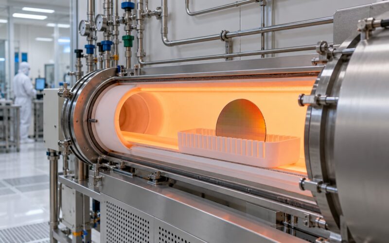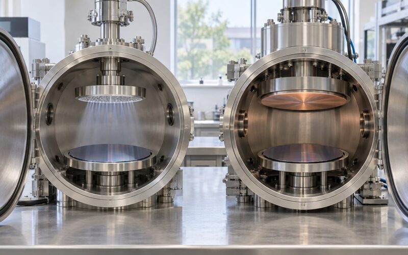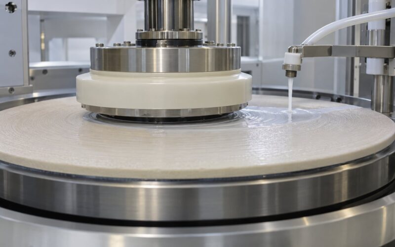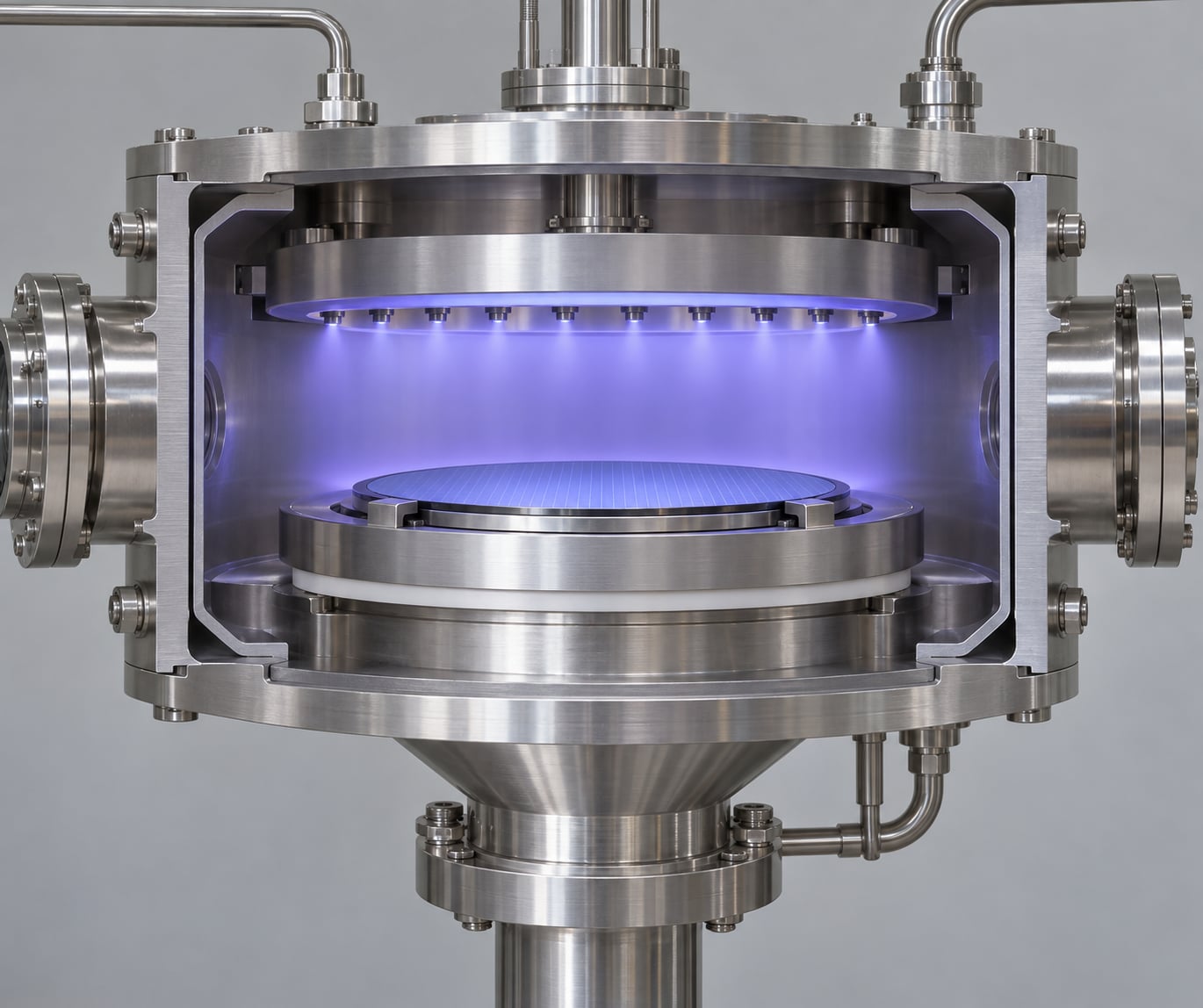
Plasma etching is a dry etching technique that removes material from a semiconductor wafer using an ionized gas, excited by radio-frequency power. Reactive neutral species etch the surface chemically into volatile byproducts, while directional ion bombardment accelerates that reaction and stops it from progressing sideways. That pairing is what lets a fab cut vertical walls and features far narrower than a photolithography wavelength.
The plasma etching process explained here runs from wafer prep to post-etch ash in seven steps, then covers the chemistries, the parameters engineers actually set, the technique choices, and the failure modes that eat yield. No RF background required.
Table of Contents
- What Is Plasma Etching?
- How the Plasma Etching Process Works
- What plasma actually is, in plain English
- The plasma etching process explained step by step
- What Are the Main Types of Plasma Etching?
- Reactive ion etching (RIE)
- Inductively coupled plasma etch (ICP-RIE)
- Deep reactive ion etching (DRIE, Bosch process)
- Cryogenic etching
- Plasma ashing and dry strip
- Atomic layer etching (ALE)
- CCP versus ICP: the key differences
- Why Are Chemistries and Gases Used?
- How Plasma Etching Controls Feature Size and Profile
- What Problems Can Cause Plasma Etching Defects?
- How Is a Plasma Etching Process Controlled and Measured?
- Frequently Asked Questions
- What is plasma etching in semiconductor manufacturing?
- Why is plasma etching used instead of wet etching?
- What is the difference between plasma etching and reactive-ion etching?
- How does anisotropy improve with plasma etching?
- What gases are commonly used in plasma etching?
- How do engineers detect the endpoint of a plasma etch?
- Conclusion
What Is Plasma Etching?
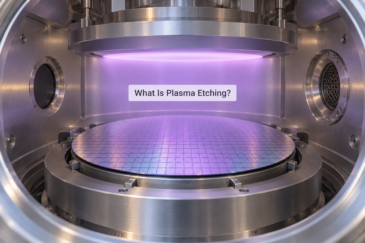
Plasma etching patterns material by turning a gas into its fourth state. The gas is ionised, reactive fragments of it strike the wafer, chemically convert the film into a compound that is volatile at low pressure, and the vacuum pumps carry that compound out of the chamber.
That is what separates it from wet etching, where liquid chemistry does the dissolving. A liquid bath attacks every exposed surface at once, so features round off as they deepen. Plasma etch can be aimed: the chemical part supplies speed, the ion part supplies aim.
| Criterion | Plasma (dry) etch | Wet chemical etch |
|---|---|---|
| Profile control | Anisotropic; vertical sidewalls at high aspect ratios | Largely isotropic; sidewalls slope and undercut |
| Smallest practical feature | Deep sub-micron, high aspect ratio trenches | Micron-scale features before profile degrades |
| Material range | Most solids, including oxides, nitrides and metals | Oxides and some metals; polymers and many films resist it |
| Patterned selectivity | Controlled with gas choice, pressure and bias | Depends on solution chemistry alone |
| Throughput | Single-wafer chambers; minutes per layer | Batch immersion; many wafers per tank |
| Waste and safety | Gas handling, abatement, RF and vacuum hazards | Liquid handling, fumes, effluent disposal |
Wet etch still wins on cost and simplicity for large, non-critical features and for cleaning steps. Etch wins wherever a pattern has to hold its shape.
How the Plasma Etching Process Works
What plasma actually is, in plain English
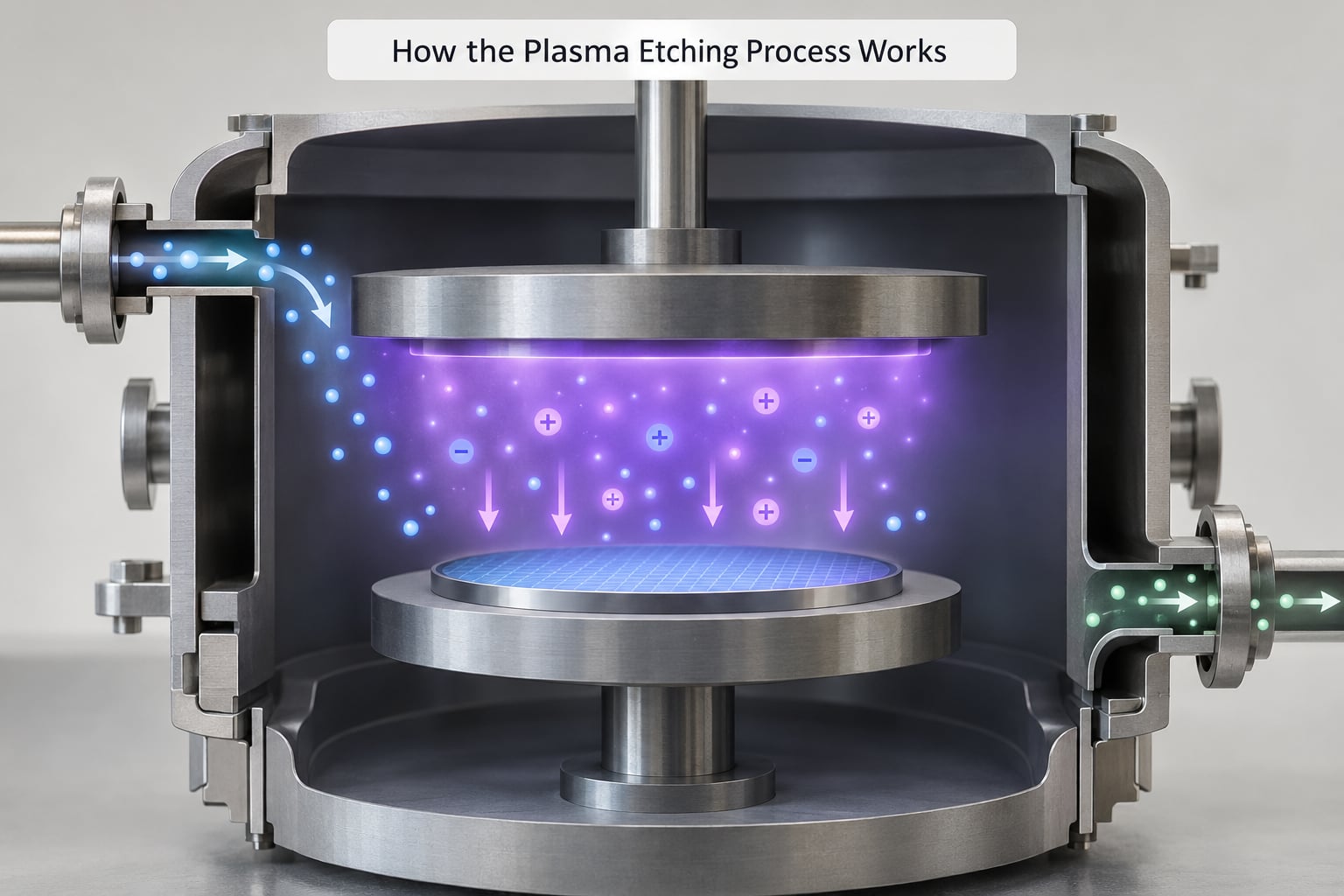
Plasma is not hot enough to melt anything. It is an ionised gas, and its usefulness comes from the fact that it contains three very different things at once:
- Free electrons. They move fast, collide with gas molecules and knock them apart.
- Ions. The stripped cores of those molecules. They are heavy, they carry a positive charge, and a bias on the wafer can steer them straight down.
- Radicals. Neutral fragments such as fluorine atoms. They hit the surface, react chemically and do most of the actual removing.
Electrons travel far faster than ions, so the wafer repels electrons more effectively than it gathers ions. The wafer charges negative on its own, creating a thin region called the sheath where ions are accelerated toward the surface. Raise the bias power and you raise the ion energy hitting the wafer; raise the source power and you raise the density of the reactive species in the bulk. Those are two different knobs, and separating them is the central trick of modern etch tools.
The plasma etching process explained step by step
- Wafer prep and mask. The wafer is cleaned, a photoresist or a deposited hard mask such as oxide or nitride defines what stays. Mask choice sets the ceiling on how deep you can go, because you cannot etch much further than the mask survives.
- Chamber pump-down and load. The wafer lands on an electrostatically clamped chuck, often over backside helium for thermal contact. The chamber is evacuated to a base pressure in the low millitorr range before any process gas enters.
- Gas introduction. Process gases are admitted at controlled flows, typically a few tens of standard cubic centimetres per minute each. Flow ratios set the chemical balance; pumping speed and throttle position then set the working pressure.
- Plasma ignition and stabilisation. RF power at 13.56 MHz, the industry standard frequency, strikes the gas. Matching networks tune the delivered power, and the engineer waits for the plasma to stabilise before the timed etch begins, because the initial transient etches at a different rate than the steady state.
- Main etch. Radicals land on the exposed film and convert it to a volatile product. Ions arrive along the sheath field, roughly perpendicular to the wafer, break surface bonds and knock atoms loose. The result is material removed downward and barely at all sideways.
- Endpoint and over-etch. The tool watches a signal tied to the etch itself and stops when the exposed material runs out. A timed over-etch follows to clear residue in the corners that endpoint cannot see, which is why over-etch time is budgeted rather than ignored.
- Pump-down, ash and clean. Gases are purged, the chamber evacuated, and a separate oxygen or fluorine step strips remaining resist in the same tool. A chamber clean at defined intervals removes polymer and sputtered metal that would otherwise drift into the next batch.
Those numbers are typical industry values for a conventional silicon tool, not specifications for any particular machine. Real ranges move with chamber geometry, layer stack and the specific reactor design, and most are held in a recipe rather than typed in by hand.
| Parameter | Typical range | What it controls |
|---|---|---|
| Source / RF power | 300 to 1500 W | Plasma density and chemical etch rate |
| Bias power | 20 to 400 W | Ion energy, directionality, mask erosion |
| Chamber pressure | 5 to 80 mTorr | Mean free path, ion directionality, sidewall passivation |
| Gas flow per channel | 5 to 100 sccm | Chemical balance and residence time |
| Chuck temperature | 0 to 80 C | Profile control and polymer build-up |
| Etch rate | 20 nm/min to several um/min | Depends entirely on film and chemistry |
What Are the Main Types of Plasma Etching?
All of them use the same chemistry-plus-bombardment idea. They differ in how the plasma is generated, how the ion direction is set, and whether the etch runs continuously or in self-limiting cycles.
Reactive ion etching (RIE)
RIE is the capacitively coupled, parallel-plate reactor. RF drives both the plasma and, through a DC self-bias that develops on the smaller electrode, the wafer. One knob controls two things at once, which is its main limitation and the reason the next type exists. RIE remains the workhorse for polysilicon gates, contacts and moderate-aspect-ratio dielectric etch, and it is the cheapest way to get a directional dry etch.
Inductively coupled plasma etch (ICP-RIE)
A coil above the chamber generates the plasma while a separate lower electrode sets bias, so plasma density and ion energy are controlled independently. That buys high etch rates at low ion energy, which means less damage to the layer underneath and better selectivity to a thin stop layer. The cost is tool complexity and a harder-to-predict sheath, so profile control takes more development.
Deep reactive ion etching (DRIE, Bosch process)
DRIE alternates a short etch phase and a short passivation phase, usually in the same chamber, hundreds of times. The etch phase clears polymer from the trench base and cuts silicon; the passivation phase coats the sidewalls with a fluorocarbon film that protects them. Net removal is directional, but each cycle leaves a small ripple, which is where scalloping on sidewalls comes from.
Cryogenic etching
The chuck is cooled with liquid nitrogen, often to minus 80 to minus 140 C. Reactive species condense on cold sidewalls and sputter far less than they do at room temperature, so the scallops left by a Bosch process largely disappear. That matters most in silicon photonics, where waveguide sidewall roughness drives optical loss. The trade-off is reduced selectivity to the masking material.
Plasma ashing and dry strip
An oxygen plasma burns resist away as carbon dioxide and water vapour. It is directional in the sense that nothing is sputtered, but it is a removal step, not a pattern transfer step, and it goes in the same chamber at the end of the run.
Atomic layer etching (ALE)
ALE is cyclical and self-limiting. A precursor adsorbs on the surface, a plasma step clears the reacted layer, and the cycle repeats. Each cycle removes a fraction of a nanometre with almost no lateral loss and almost no ion damage. It is the most precise option and the slowest, and it competes with continuous plasma etch mainly at extreme selectivity requirements.
CCP versus ICP: the key differences
| Criterion | CCP / RIE | ICP-RIE |
|---|---|---|
| Coupling mechanism | Capacitive, between parallel plates | Inductive coil above a dielectric window |
| Control of density vs ion energy | Coupled; one knob moves both | Decoupled; source sets density, bias sets energy |
| Plasma density | Lower | Up to two orders of magnitude higher |
| Etch rate | Moderate | High at low bias |
| Mask and stop-layer selectivity | Lower at higher bias | Higher, because bias can stay low |
| Damage to underlying layers | More, from energetic ions | Less, for the same etch rate |
| Cost and complexity | Lower; simpler to maintain | Higher; more process development |
| Typical use | Gate etch, contacts, dielectric, ashing | High-aspect-ratio oxide, poly and metal, low-damage layers |
The decision rule is short: if you can hit your etch rate at low bias and need selectivity or low damage, go inductive. If the layer is simple and cost matters, capacitive is enough.
Why Are Chemistries and Gases Used?
Gas choice decides what chemistry is available on the surface. The etch only works if the reaction product is volatile enough to leave at chamber pressure, and every chemistry is chosen to make one specific product volatile.
| Layer to etch | Typical gases | Why |
|---|---|---|
| Silicon, polysilicon | SF6, CF4, CHF3, Cl2, HBr | Fluorine yields volatile SiF4; chlorine and bromine give higher selectivity and polymer-free sidewalls |
| Silicon dioxide | CF4, CHF3 with O2 or Ar | Fluorocarbon chemistry; adding O2 raises selectivity to the underlying stop layer |
| Silicon nitride | CF4, CHF3, NF3 | Fluorine converts it to a volatile species; NF3 avoids polymer build-up |
| Aluminium | Cl2 or BCl3 with H2 | Aluminium halides are volatile at low pressure; fluorine fails here because the fluorides are not |
| Copper, tungsten | Cl2, HBr, SF6 | Chlorine and bromine volatilise the metal; extra hydrogen suppresses re-deposition |
| Photoresist and organics | O2 | Oxidises carbon to CO2 and H2O; nothing to sputter |
| Physical clean or bombardment | Ar | Nobles gas, no chemistry, pure momentum transfer |
Bromine chemistries such as HBr sit between fluorine and chlorine: less aggressive than fluorine, more selective than chlorine, and common in polysilicon gate etch where the stop layer is a gate oxide only a nanometre or two thick.
Fluorine chemistries also do something chlorine does not: they grow a fluorocarbon polymer on the sidewall that passivates it. That film is why a fluorine etch can hold a vertical wall. It is also why fluorine steps tend to leave residue, and why an oxygen clean follows so often.
How Plasma Etching Controls Feature Size and Profile
Feature size is set by the mask and held by how much sideways removal you allow. Two numbers describe the result: anisotropy, the ratio of vertical to lateral etch, and selectivity, the etch rate of the target divided by the etch rate of the mask or stop layer.
They trade against each other. More bias power pushes the etch more vertical and also chews the mask faster. More fluorine passivates the sidewall but builds polymer you then have to clean. There is no setting that maximises everything, only a process window where the layers you care about stay inside their budgets.
Aspect ratio is where the physics turns on itself. In a deep trench, reactive neutrals hit the bottom at a glancing angle, so their local flux drops as the trench deepens. Ions still arrive near-perpendicular. So narrow, deep features etch slower than open areas, which is called aspect-ratio-dependent etching, or etch lag. Pattern density does the same thing at a larger scale: a dense array of trenches depletes local reactant supply and etches slower than an isolated trench of the same width.
Profile shape follows from the balance. A bowed sidewall usually means the etch ran long with too much isotropic chemistry. A tapered top means the mask eroded. Vertical walls that break through into the layer below mean selectivity was never high enough for the depth you needed.
This is why etch depth alone is a poor specification. Fabs judge a step on the critical dimension at the base of the feature, because a nanometre of error in gate length translates directly into a change in how fast the finished transistor switches.
What Problems Can Cause Plasma Etching Defects?
Every one of these has a mechanical cause. When something looks wrong on an SEM cross-section, the fix is usually a process parameter or chamber condition, not a new mask.
| Symptom | Likely cause | What to change |
|---|---|---|
| Undercut and bowed sidewalls | Too much neutral chemistry relative to ion flux; over-etch time too long | Raise bias, raise pressure slightly, shorten over-etch, switch to a more polymer-forming gas mix |
| Notching at the trench base | Charging of the feature; positive ions pool at the base and etch sideways | Reduce etch time, lower pressure, add a charge-control step at the start of the etch |
| Microtrenching just below the trench | Ions reflect off the trench corner at a shallow angle and concentrate there | Reduce bias at the start, raise pressure to thermalise the ion angular distribution |
| Scalloped sidewalls | Cyclical etch and passivation phases in a Bosch process | Reduce cycle time at the etch end, or move to cryogenic etch where passivation does not etch back |
| Residue or grass | Fluorocarbon polymer left behind; chamber walls coated | Add an oxygen descum, retune gas ratios to lower carbon, clean the chamber on schedule |
| Etch rate drift over a lot | Chamber seasoning: polymer and sputtered metal accumulate | Shorten the clean-to-production interval, verify matching, check the showerhead for blockage |
| Pattern-dependent rate | Loading effect: a dense pattern consumes more reactant than an open one | Adjust gas flow for pattern mix, reduce etch time, or split the exposure into two passes |
| Mask erosion | Ion bombardment at high bias on an organic resist | Move to a hard mask, lower bias, raise fluorine polymer passivation |
| Damage or charging on a thin layer | Ion impact and UV-generated charge on the film under the mask | Drop bias power, separate into two steps, or switch to a low-damage inductively coupled recipe |
Two structural limits are worth knowing before you chase a recipe. Pattern loading is expected, not a defect: it is a first-order effect of how much material is being removed. And chamber condition moves every number in the process, so comparing a recipe written six months ago against today’s tool is not a like-for-like measurement.
How Is a Plasma Etching Process Controlled and Measured?
Etch is qualified statistically, not by eye. The workflow runs from a screening design of experiments to a response-surface model, then into production control with statistical process control charts on endpoint time and etch depth.
Chamber conditioning. Every tool has a clean cycle and a production cycle. Conditioning builds a known surface layer of polymer or oxide on the chamber walls, which becomes the boundary condition for the etch. Deviating from the cycle changes the etch rate.
Endpoint detection. Three methods cover most work. Optical emission monitoring watches a narrow wavelength band of light from excited species; the signal drops when the material being etched runs out. Interferometry tracks a reflected laser off the wafer and converts phase change into etched thickness. Bias monitoring watches the DC self-bias, which shifts when the surface chemistry changes. None of them is universally best, which is why tools often carry two at once.
Wafer-level measurement. SEM cross-sections check profile and CD on a sampling plan. Timed tools measure a monitor film between product layers. Profilometry and ellipsometry check blanket films. A process that reads clean at endpoint can still be off by tens of nanometres, so the film measurement is not optional.
Statistical process control. Endpoint time and monitor thickness are trended per chamber. Drift in either predicts the failure before the defect metrology does, which is the whole point of running an etch tool this way.
Frequently Asked Questions
What is plasma etching in semiconductor manufacturing?
Plasma etching removes material from a wafer using a gas turned into plasma by RF power. Reactive neutral species react chemically with the film to form volatile byproducts that vacuum pumps carry away, while directional ions bombard the surface to speed the reaction and hold the profile vertical. It is the main pattern-transfer step in chip fabrication.
Why is plasma etching used instead of wet etching?
Liquid chemistry attacks every exposed surface at once, so a wet-etched trench ends up sloped and undercut as it deepens. Plasma etch separates speed from aim: radicals do the removing and ions supply direction. That is why gates, vias and deep trenches are defined by dry etch, while wet etch stays useful for large non-critical features and cleaning.
What is the difference between plasma etching and reactive-ion etching?
Plasma etching is the family name for any dry etch driven by an ionised gas. Reactive ion etching is one specific reactor style: a capacitively coupled parallel-plate chamber where one RF source drives both the plasma and the wafer bias. So RIE is a plasma etch, but not every plasma etch is RIE.
How does anisotropy improve with plasma etching?
Anisotropy is vertical etch divided by sideways etch. Plasma etch improves it with directional ion bombardment driven by the sheath and with sidewall passivation, where a fluorine-bearing polymer film coats and protects the vertical walls while the trench base stays exposed. More bias power and higher pressure both steepen the profile, at the cost of mask erosion and sidewall bowing.
What gases are commonly used in plasma etching?
SF6, CF4 and CHF3 for silicon, oxides and nitrides. Cl2, BCl3 and HBr for aluminium, copper and tungsten. O2 for photoresist removal and descum. Ar for physical bombardment with no chemistry. The choice always comes down to making one specific reaction product volatile at chamber pressure; if the product is not volatile, the etch stops.
How do engineers detect the endpoint of a plasma etch?
Optical emission monitoring watches a wavelength tied to the species being consumed, interferometry measures reflected laser phase change as thickness drops, and bias monitoring watches the DC self-bias shift when surface chemistry changes. The tool stops when the signal moves, then runs a timed over-etch to clear corners the signal cannot see.
Conclusion
If you take one mental model away, make it this: plasma etching is a chemical reaction with a steering wheel attached. The chemistry decides what can be removed at all, and the ions decide where it stops.
Start with the four ideas that everything else hangs off. Directionality comes from the sheath and bias, selectivity is a ratio you tune rather than a property you find, anisotropy comes from balancing passivation against bombardment, and the process window closes as features get deeper and masks get thinner.
From there, learn the sequence: prep, pump down, gas in, strike, etch, endpoint, ash. Once the sequence is second nature, the technique choice, the gas table and the failure-mode list stop being trivia and start being the levers you actually pull.