Photolithography is the process of using light to transfer a circuit pattern from a photomask onto a light-sensitive coating called photoresist, which sits on a silicon wafer. The exposed resist changes how it behaves in developer, and whatever survives becomes a stencil for etching or deposition. Every transistor you have ever read about gets its shape this way.
That is the whole idea in two sentences. The rest is detail, and the detail is where beginners usually get stuck, because most explanations skip straight to jargon like numerical aperture and chemically amplified resist without ever showing what the wafer looks like between steps.
So here is the mental model first: you coat a wafer in a light-sensitive plastic, shine a focused light through a patterned glass plate, wash away the soft parts, and use the hardened pattern as a stencil to carve the material underneath. Print a stencil, use it as a cookie cutter. Once that image is in your head, the eight steps below fall into place almost on their own.
If you want the terminology in one place before you start, jump to the parts and glossary section. If you want the flow first, read straight through. Either way, you should be able to explain the cycle to someone else after this article.
Table of Contents
- Photolithography Process Explained for Beginners: What Is It?
- Why Is Photolithography Important in Semiconductor Manufacturing?
- How Does the Photolithography Process Work?
- Photolithography Process Explained for Beginners: The Core Steps
- 1. Cleaning and wafer preparation
- 2. Adhesion promotion (vapor prime)
- 3. Spin coating the photoresist
- 4. Soft bake (pre-bake)
- 5. Alignment and exposure
- 6. Post-exposure bake (PEB)
- 7. Development
- 8. Etch, inspection, and resist stripping
- What Are the Main Parts of a Photolithography System?
- What Is the Difference Between Positive and Negative Photoresist?
- Which Photolithography Methods Are Used in Chip Production?
- How Do Engineers Control Feature Size and Alignment?
- What Are the Most Common Photolithography Problems?
- Frequently Asked Questions
- What does photolithography do in semiconductor manufacturing?
- Is photolithography the same as photoprinting?
- What is the difference between a photomask and a wafer?
- Why is a photoresist used during photolithography?
- What happens after a photoresist pattern is developed?
- How do engineers make photolithography patterns smaller?
- Conclusion: Start With the Patterning Flow
Photolithography Process Explained for Beginners: What Is It?
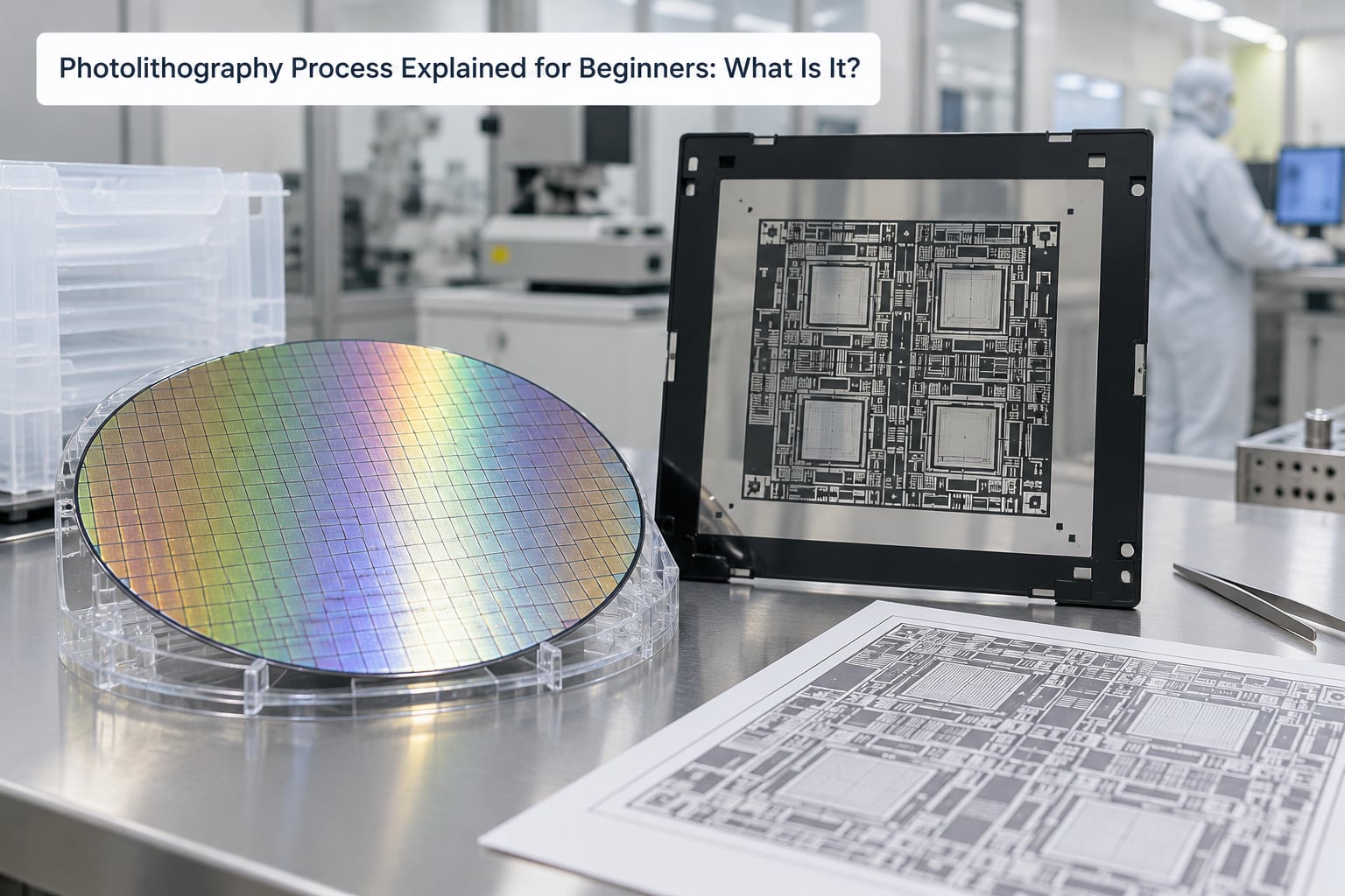
Photolithography (also called optical lithography or just lithography) is a microfabrication technique that uses light to transfer a geometric pattern from a photomask onto a light-sensitive chemical coating, the photoresist, spread across a substrate. After exposure and development, the resist pattern controls which parts of the underlying thin film or substrate get etched, doped, or deposited on. It is how every geometric shape in a chip gets defined.
The word itself is a clue. Photo means light, and lithography literally means stone writing. It is the same root as lithography in printing, where a limestone plate takes ink where the image is.
Two things make photolithography unusual compared with other fabrication methods. First, it is additive to the pattern, not subtractive: you build up the geometry layer by layer rather than carving one block of material. Second, it is repeatable. The exact same mask pattern can be printed onto hundreds of wafers in a row, which is what makes mass production possible at all.
Within wafer fabrication, lithography is one step inside a much larger cycle. Deposition lays down films, photolithography defines where those films get modified, etching removes the unwanted material, and chemical mechanical polishing flattens the surface again before the next layer goes down. Lithography is the step that decides where everything else happens, which is why it gets the most attention and the most money.
You will also hear the term used far outside chipmaking. Photolithography patterns printed circuit boards, microfluidic channels, MEMS devices, optical gratings, antennas, and even the pixels on some display sensors. The chemistry and optics scale down, but the logic stays identical.
Why Is Photolithography Important in Semiconductor Manufacturing?
Because every geometric feature in a modern chip is defined by light. Not most of them, not some of them. All of them.
To build a transistor, the process engine coats the wafer in resist, prints the shape of the gate electrode, etches that shape into the layer below, and strips the resist away. To build the copper wiring that connects millions of transistors, the same sequence repeats with a different mask and a different set of materials. A current-generation logic wafer goes through the lithography and etch cycle roughly 30 to 50 times, each pass adding one more level of structure.
That repetition is why lithography dominates the cost and the schedule of a fab. The tool is the bottleneck, the masks are expensive, and every extra pass means more time on the machine. Improving lithography, not adding new materials, is what has delivered most of the density gains the industry is famous for.
The second reason is precision of placement. Each new layer has to line up with the layers underneath it, sometimes to within a few nanometres, across a wafer 200 or 300 millimetres wide. Nobody could hand-align that. Photolithography uses optical alignment marks and automated stage correction, which is why the machines have a stepper or a scanner built in.
The third reason is scale. The same mask and the same process recipe can be repeated on every wafer in a lot, and across hundreds of lots, for years. That repeatability is what turns a laboratory technique into an industry. One patterned wafer might be a curiosity; a thousand identical patterned wafers are a product.
And lithography is not only for silicon. Printed circuit board makers use photosensitive film to etch copper traces. MEMS and microfluidics researchers use it to release tiny movable structures and to carve channels into glass. Photonics groups use it to make diffraction gratings and waveguides. Nanoscale printing, solar cell manufacturing, and some display fabrication all borrow the same flow.
How Does the Photolithography Process Work?
At the highest level the process is a loop. You prepare a clean surface, cover it in resist, bake the resist dry, align a mask over it, expose it, bake again, develop it, transfer the pattern into the material below, strip the resist, and clean up. Then you flatten the surface and do it all again for the next layer.
Two ingredients make it work. The first is the resist, a polymer whose solubility in developer changes when light hits it. The second is the mask, a quartz plate with a chrome pattern that acts as a stencil for the light. Everything else in a modern fab exists to make those two do their job accurately and repeatably.
Light only carries so much detail, so engineers have spent decades shrinking the wavelength, raising the numerical aperture, and reshaping the wavefront with computational corrections. Those techniques are covered further down. For now, the practical flow matters more than the optics.
Photolithography Process Explained for Beginners: The Core Steps
Below is the end-to-end cycle in the order a wafer actually moves through the tools. For a beginner reading this for the first time, step one is the step everyone forgets exists, and it is the step that decides whether the rest works.
1. Cleaning and wafer preparation
The wafer is cleaned to remove particles, organic residue, and dissolved metals, then rinsed and dried. In a fab this often means a dilute chemical clean followed by an RCA-style clean, which uses hydrogen peroxide and ammonia to strip organics and hydrochloric acid and hydrogen peroxide to strip metals.
The reason is simple. Any speck of dust left on the surface becomes a defect copied onto every chip, and any metal ion left behind can degrade a thin gate oxide later. You cannot print a good pattern onto a dirty surface. The visible result you are aiming for is a uniformly hydrophilic, particle-free wafer; the measurement is particle count and surface contact angle.
2. Adhesion promotion (vapor prime)
Before resist goes on, the surface is treated with an adhesion promoter, usually hexamethyldisilazane, or HMDS, delivered as a vapor. HMDS bonds to surface hydroxyl groups and leaves a hydrophobic silicon-terminated surface, which helps the resist spread evenly and stick.
Skip this and you get the classic beginner failure: a pattern that looks perfect after exposure but lifts off in a sheet during development or etch. The adhesion promoter is a chemical primer, not a cleaning step, and it is cheap insurance.
3. Spin coating the photoresist
Liquid resist is dispensed onto the centre of the spinning wafer. Centrifugal force flings the liquid outward into a film, and the film thins as solvent evaporates. A typical spin runs somewhere around 1200 to 4800 rpm for roughly 20 to 60 seconds, and final thickness is set by spin speed, resist viscosity, and how much solvent was in the formulation.
The visible check is a smooth, colour-uniform film with no interference banding and no visible ridges. In a fab, the coater sits inside a wafer track, a sealed machine that carries the wafer through coat, bake, develop, and sometimes strip, so the wafer never has to leave a controlled environment.
4. Soft bake (pre-bake)
The wafer is heated, typically around 90 to 100 degrees Celsius for a minute or two, to drive off the remaining solvent and stabilise the film. This is the soft bake, and its job is to make the resist a solid coating rather than a sticky film that would smear or shift.
Remove it and the resist keeps moving. Overdo it and the resist is baked too hard to develop cleanly. The number that matters is the remaining solvent left in the film, measured by weight, and fabs hold a narrow window around it.
5. Alignment and exposure
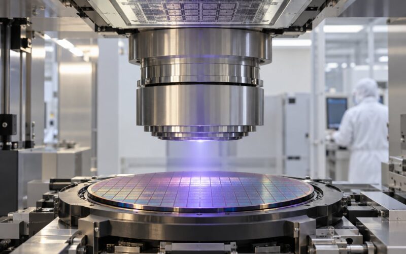
The wafer goes into a mask aligner, stepper, or scanner. A reticle, the small patterned plate that carries one die pattern, is brought to within microns of the resist surface. The tool finds previously printed alignment marks, computes the correct offset, and fires a pulsed light source through the reticle.
Where light passes through, the resist molecules break or rearrange. Where the chrome blocks it, nothing happens. The duration, dose, and focus of that flash are the three numbers process engineers spend the most time tuning.
6. Post-exposure bake (PEB)
Most modern production resists are chemically amplified. Exposure creates a small number of acid molecules, and this bake gives that acid a chance to catalyse a chain reaction across the polymer, effectively amplifying one photon into a large chemical change.
The PEB is short, often 60 to 120 seconds, but it is the most sensitive bake in the cycle because it feeds an autocatalytic process. A few degrees or a few seconds out of spec is enough to lose line width, which is why a fab controls it tightly.
7. Development
The wafer goes into a developer, commonly a solution of tetramethylammonium hydroxide, or TMAH, for positive resists. The exposed, acid-catalysed regions dissolve away, and the unexposed regions stay. Rinse and dry follow immediately.
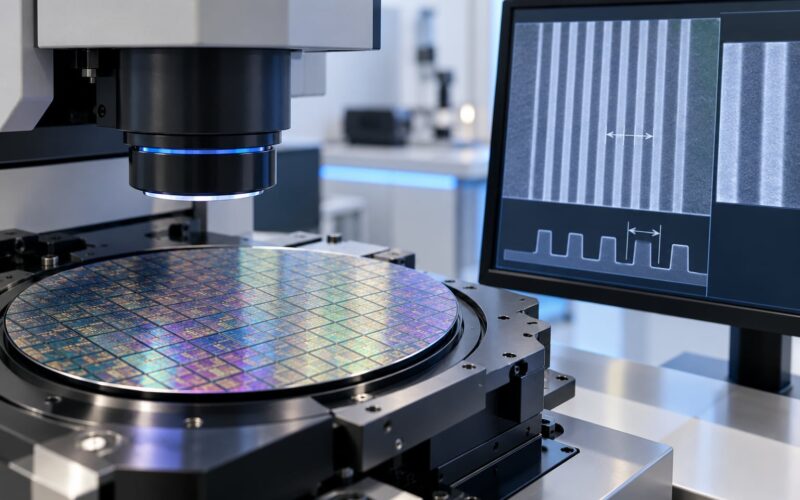
This is the moment the pattern becomes visible. On a positive resist you are left with raised lines where the mask blocked light; on a negative resist you are left with raised lines where light passed. A quick check under an optical microscope shows whether the lines have the right width and whether anything is broken, bridged, or missing.
8. Etch, inspection, and resist stripping
The resist pattern is now a stencil. An etch, usually a plasma or dry etch, removes the exposed material underneath and copies the pattern into the film or substrate. The wafer is inspected at several points along the way with optical and electron-beam metrology, then the resist is stripped, usually by an oxygen plasma ashing step followed by a wet clean.
Etching is where most beginners first lose their results. The pattern looked fine in developer, then the etch undercut it, or the resist was too thin to survive the plasma, or the etch was too selective and stopped early in the layer below. After stripping, the surface is flattened and the whole cycle begins again for the next layer.
Here is the same flow compressed into one view, with the tool and the number that matters at each stage.
| Step | What happens | Typical tool | Key parameter |
|---|---|---|---|
| 1. Clean | Particles, organics and metals removed | Wet bench or single-wafer clean | Particle count, contact angle |
| 2. Prime | Adhesion promoter vapour deposits on surface | Vapour prime module | HMDS dose and time |
| 3. Spin coat | Liquid resist spun into a uniform film | Wafer track coater | 1200-4800 rpm, target thickness |
| 4. Soft bake | Solvent driven off, film stabilised | Wafer track hot plate | 90-100 C, 1-2 minutes |
| 5. Align and expose | Reticle aligned, pulsed light prints pattern | Stepper or scanner | Dose in mJ/cm2, focus, overlay |
| 6. PEB | Acid catalyses polymer change, amplifies image | Wafer track hot plate | 60-120 C, 60-120 seconds |
| 7. Develop | Exposed resist dissolves, pattern revealed | Wafer track developer | Time, temperature, chemistry |
| 8. Etch and strip | Pattern transferred into film, resist removed | Plasma etcher, asher | Selectivity, rate, bias |
What Are the Main Parts of a Photolithography System?
You can break any photolithography setup into seven pieces, whether it is a research cleanroom or a full production fab. Knowing which part does what removes most of the vocabulary confusion beginners run into.
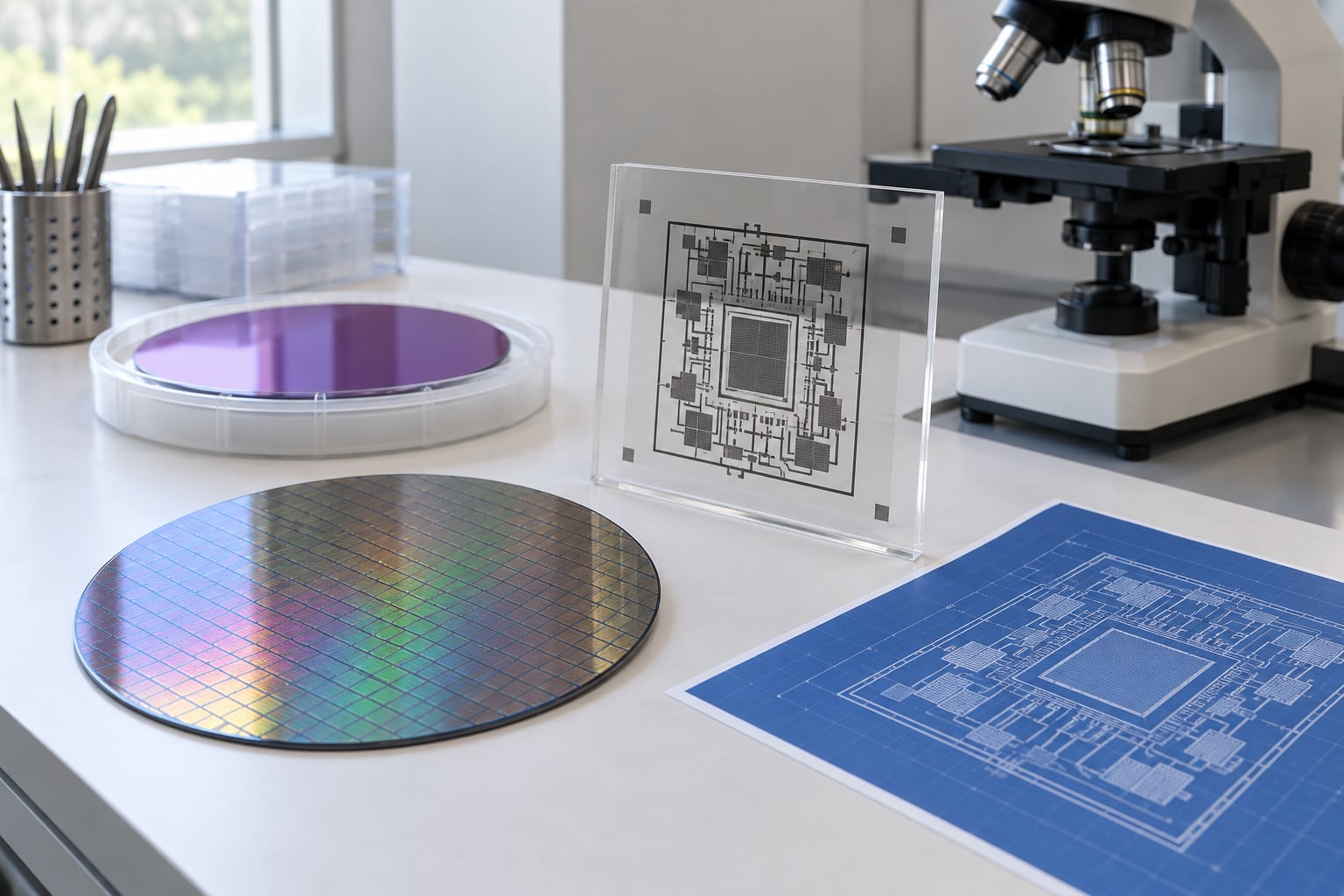
The substrate is the material being patterned, usually a silicon wafer but sometimes glass, ceramic, or a flexible film. The photoresist is the light-sensitive polymer coating, applied by spin coating or by a dry film that behaves more like a sticker sheet. The photomask, or reticle, is the quartz and chrome stencil carrying the pattern; the mask set for one chip can contain hundreds of them.
The exposure tool, called a mask aligner at research scale and a stepper or scanner in production, holds the light source, the optics, the reticle stage, and the wafer stage in one vibration-controlled frame. The alignment system reads marks printed in earlier layers and corrects the wafer position before exposure. The developer module applies and rinses the chemistry, and metrology equipment checks what actually happened.
A few more terms will show up repeatedly. A cleanroom is a space where particle concentration is controlled by filtration, airlocks, and full-body suits, because a single speck in the air is a defect. Pattern transfer is the general term for etching or implanting through the resist stencil. Critical dimension, or CD, is the width of a printed feature, and controlling it is the central goal of the whole discipline.
| Term | Plain-English meaning |
|---|---|
| Wafer | The thin silicon disc holding hundreds of identical chips |
| Substrate | Whatever surface is being patterned |
| Photoresist | The light-sensitive polymer film that records the pattern |
| Photomask / reticle | The patterned glass stencil that shapes the light |
| Mask aligner | The machine that aligns the reticle and exposes the resist |
| Stepper | An aligner that exposes one die at a time in a grid pattern |
| Scanner | An aligner that sweeps a slit across the whole wafer |
| Developer | The chemical that removes exposed resist |
| PEB | Post-exposure bake, which amplifies the exposed image |
| Etch | The step that copies the resist pattern into the material below |
| DUV / EUV | Deep ultraviolet and extreme ultraviolet light sources |
| Numerical aperture | How wide the focusing cone is, which sets the smallest printable line |
What Is the Difference Between Positive and Negative Photoresist?
The difference is which part of the resist the light makes soluble. That single choice flips the polarity of everything you print, and getting it backwards is a common beginner error that produces a pattern in exactly the wrong places.
In a positive resist, light breaks polymer chains and makes the exposed region thinner, softer, and more soluble in developer. The exposed area washes away, so the raised features that remain are the ones the mask blocked. In a negative resist, light cross-links the polymer instead, hardening the exposed area so it survives development while the unexposed area dissolves.
Almost all modern production IC work uses positive resist. It offers better resolution and better control of line width, and it is the reason most mask drawings look the same way the finished chip does. Negative resist is still common in thick-film power devices, in solder mask printing, and in some packaging work, and it is often the easier chemistry for very thick layers.
| Feature | Positive resist | Negative resist |
|---|---|---|
| Effect of light | Breaks polymer chains, exposed area softens | Cross-links polymer, exposed area hardens |
| After development | Exposed area removed, pattern left where mask blocked light | Exposed area remains, unexposed removed |
| Developer | Commonly TMAH | Organic solvent such as PNB |
| Resolution | Better line width control, used for fine features | Suits thicker films, less precise |
| Typical use | IC layers, MEMS, microfluidics | Thick films, power devices, solder mask |
One practical note. The mask and the pattern are mirror images of each other, because projection optics flip the image on the way to the wafer. A mask that looks reversed is normal, and it is not a manufacturing defect.
Which Photolithography Methods Are Used in Chip Production?
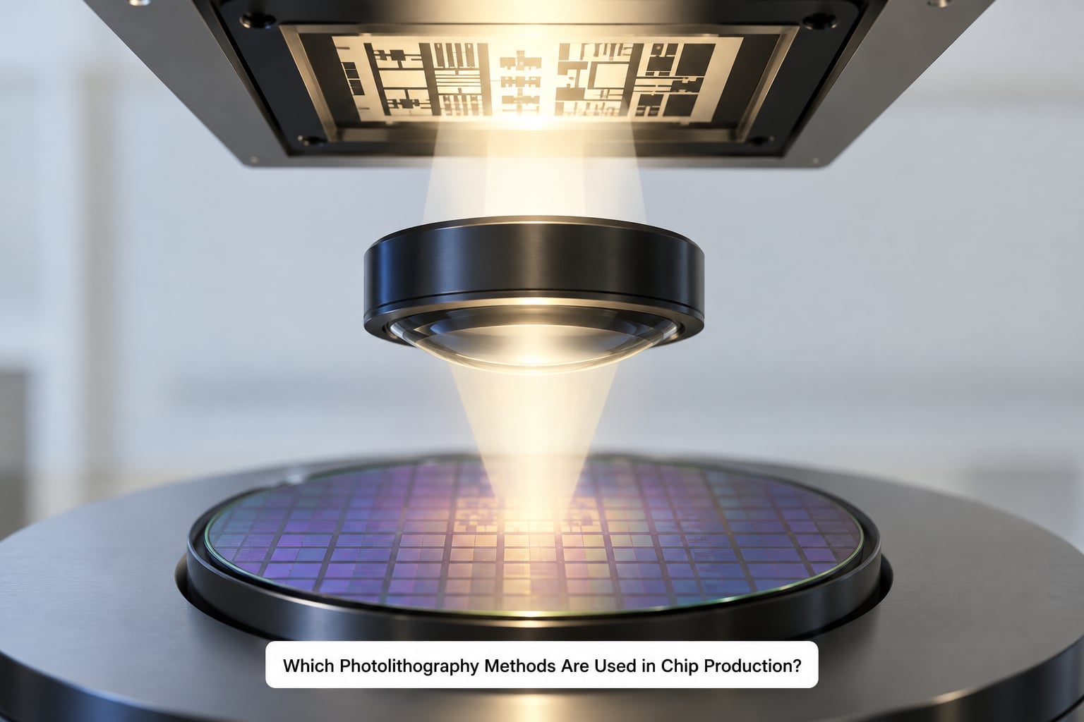
There are three classic ways to put a mask image onto a resist, and they differ in how close the mask sits to the wafer. The closer the gap, the higher the resolution and the higher the risk of a defect printing from the mask itself.
In contact printing, the mask touches the resist. The resolution is excellent, but any particle on the mask or the wafer becomes a broken line in every die, which is why contact printing essentially disappeared from mainstream production. In proximity printing, the mask hovers a few microns above the wafer, protecting the pattern at the cost of some resolution. In projection printing, a lens system projects a focused image of the mask with the mask many centimetres away, and this is how essentially all production lithography is done.
Projection tools come in two flavours. A stepper exposes one die at a time, stepping the wafer in a grid, and it dominates research and mature-node work. A scanner exposes a narrow slit and sweeps it across the whole wafer, which keeps the field of view small enough to hit very high numerical apertures, so scanners took over the leading edge.
Light source choices define the node you can reach. Mercury lamps at 365 nm and i-line at 365 nm handled older generations. KrF excimer at 248 nm, then ArF at 193 nm, pushed deep ultraviolet through successive nodes. Immersion lithography puts a droplet of water between the lens and the wafer, which raises the effective numerical aperture by increasing the refractive index of the medium and squeezes out more detail at the same wavelength. EUV at 13.5 nm is the current approach for the smallest layers.
| Light source | Wavelength | Typical minimum feature | Notes |
|---|---|---|---|
| Mercury lamp, g-line and i-line | 436 nm / 365 nm | Around 1 micron | Irradiation, thick films, older nodes |
| KrF excimer | 248 nm | Around 130 nm | DUV, retired at the leading edge |
| ArF excimer, dry | 193 nm | Around 90 nm | Still used for many interconnect layers |
| ArF immersion | 193 nm | Around 50 nm and below | Water between lens and resist raises NA |
| ArF dry multiple patterning | 193 nm | Around 15-20 nm class | Two exposures plus a cut process, expensive |
| EUV | 13.5 nm | Below 10 nm class | Reflective optics, masks also reflective |
Beyond optical lithography there are other approaches. Electron-beam lithography writes patterns with a focused electron beam and no mask at all, which is maskless and superb for prototyping, but far too slow for volume production. Nanoimprint lithography presses a moulded pattern into a resist and is used in some patterning and optics work. Multiple patterning is not a wavelength at all but a workaround: splitting one dense layer into two or three overlapping lithography passes so each can be printed with a simpler mask. It works, and it is expensive in mask count, process steps, and yield.
Mask data is prepared with computational lithography, which is software that pre-distorts the mask artwork to compensate for lens and resist effects. Optical proximity correction rounds corners that the optics would round anyway and inserts sub-resolution features so the printed shape matches the intended one. Mask error correction and source optimisation work on the same idea from the other end, shaping the illumination instead of the mask. It is not a beginner topic, but it explains why mask files look nothing like the circuit layout.
How Do Engineers Control Feature Size and Alignment?
Feature size comes down to one equation, and then to a handful of process controls around it. The Rayleigh criterion relates the smallest printable feature to three things: the wavelength of the light, the numerical aperture of the lens, and a process factor k1 that captures how well the process is tuned. Shorter wavelength, wider cone, better tuning, and the line gets smaller.
Numerical aperture is worth pausing on. It is the measure of how wide an angle the lens collects light over, written as n times the sine of the half-angle. A larger NA focuses tighter, but it also narrows the depth of focus, the range over which the image stays sharp. At a given NA, using a shorter wavelength buys you resolution without shrinking the focus window, which is why the industry chased 193 nm and then 13.5 nm.
Chromatic aberration is the reason nothing works with a simple lens. Different colours refract differently, so a naive lens blurs the image. Excimer lasers emit one narrow spectral line, which removes most of that problem, and remaining errors are handled by the projection optics and by computational correction in the mask data.
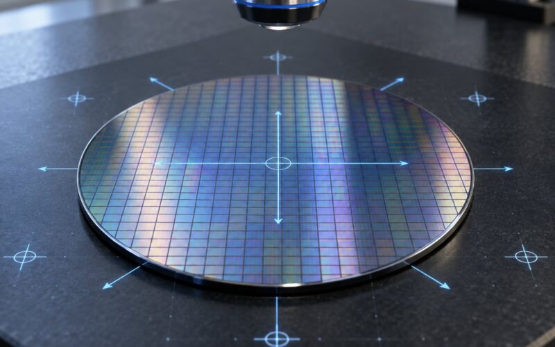
Alignment is the other half. Each layer must sit on top of the previous one, and the tolerance for that overlay error is a fraction of the smallest feature. The aligner reads cross-shaped alignment marks printed in earlier layers, compares them to a target, and adjusts the wafer stage by fractions of a micron before firing the light. Modern tools correct for wafer distortion across the full 300 mm surface, because a wafer is not perfectly flat and a rigid stage cannot compensate on its own.
Resist chemistry supplies the last part of the control. Contrast measures how sharply the resist switches from soluble to insoluble; high contrast gives a steeper profile, which transfers more cleanly into the material below. Aspect ratio matters too, because a tall narrow feature is harder to etch straight. Process engineers spend their careers inside the process window, the box inside which dose, focus, temperature, and timing can vary and the chip still works.
What Are the Most Common Photolithography Problems?
Almost every lithography failure shows up in the same handful of ways. Learning to read them is more useful than memorising recipes.
Focus error is the first suspect whenever lines look soft or widths vary across the field. If the wafer is not flat, or the stage is tilted, part of the exposure lands outside the depth of focus and the pattern blurs. Wafers get flattened with a filler layer between layers specifically to prevent this, which is why planarisation is such a big part of modern processes.
Overlay error means a pattern printed in the wrong place relative to the one below it. The cause is usually alignment marks that are dim, damaged, or already etched away, or a tool whose stage repeatability has drifted. A misaligned contact or via can short two nets together, and a chip with one shorted net is a dead chip.
Contamination on the resist does several kinds of damage at once. Particles block the light and print as pinholes or as missing resist. A single defect counts as a defect, and at 50 cycles per wafer the cumulative defect budget across a chip is what determines whether a wafer is worth processing further.
Reflections and standing waves cause patterns that look correct in shape but wrong in detail, especially on large open areas. Light reflecting off the film below the resist interferes with the incoming light, creating ripples in the dose. Resists and films are given anti-reflective coatings to suppress it, and the effect is more visible on dense line-and-space patterns than on isolated lines.
Development problems look like lifting, residue, or ragged edges. Lifting is almost always an adhesion problem, which is why the HMDS prime exists. Residue is usually a dose or time problem, where part of the resist never fully dissolved. T-shaped profiles and rounded tops point to resist chemistry or a focus issue in the exposure.
Etching problems are the most common way a good pattern turns into a bad chip. Selectivity, the ratio of etch rate in the material you want to remove versus the material you want to keep, determines whether your resist survives long enough. Anisotropy, how vertical the sidewalls are, determines whether a line stays the width you printed. Isotropic wet etch undercuts laterally, which is fine for some jobs and ruinous for others. Dry plasma etch is far more directional, which is why it replaced wet etching for most integrated circuit steps, and it is also harsher on the resist, which is why hard masks exist.
For anyone trying this outside a fab, the pattern transfer step is where home results usually fail. Hobbyists working with printed circuit boards report that dry film photoresist, the kind that behaves like a sticker, is the easiest entry point, and that a high-resolution printed or photographic mask is the standard workaround for not owning a mask aligner. Mask alignment is the part people find hardest to do by hand, and a mismatch there shows up immediately in the etch.
Frequently Asked Questions
What does photolithography do in semiconductor manufacturing?
Photolithography defines where every other process step acts on a chip. Light through a patterned mask changes a light-sensitive coating called photoresist, and the developed resist pattern tells the etch or deposition step which parts of the wafer to modify. A modern logic wafer goes through that cycle roughly 30 to 50 times, once for each layer of transistors and interconnect.
Is photolithography the same as photoprinting?
The name comes from the same root, and the physics is similar, but the precision is not comparable. Screen and inkjet printing lay down patterns tens of microns thick. Photolithography prints features measured in nanometres using light, optics, and chemistry, and the pattern it produces is usually used as an etch stencil rather than as the final image.
What is the difference between a photomask and a wafer?
A photomask, or reticle, is the stencil that shapes the light. It is a flat plate of quartz coated with a chrome pattern, and it never touches the wafer. The wafer is the silicon disc being manufactured, and it carries many identical copies of a chip. One reticle can expose hundreds of thousands of die across many wafers.
Why is a photoresist used during photolithography?
The resist is the recording medium, because the pattern has to end up somewhere solid before anything can be carved. Light alone cannot etch silicon. The resist captures the image chemically, survives the etch, and is then stripped away, which lets a fragile optical pattern do the work of a hard stencil.
What happens after a photoresist pattern is developed?
The developed resist is a stencil sitting on top of the material you want to pattern. A wet or dry plasma etch removes the exposed areas underneath and copies the pattern down into the film or the substrate. The wafer is inspected for defects, the resist is stripped with an oxygen plasma ashing step and a wet clean, and the surface is flattened before the next layer begins.
How do engineers make photolithography patterns smaller?
Three levers do most of the work. A shorter wavelength resolves smaller features, following the Rayleigh criterion. A higher numerical aperture focuses a wider cone of light onto the resist. A lower process factor k1 comes from better optics, computational mask correction, and tuned resist chemistry. Once those are exhausted, engineers use multiple patterning, splitting one layer into several simpler exposures.
Conclusion: Start With the Patterning Flow
Photolithography in one line: coat a wafer with light-sensitive resist, print a pattern through a mask, develop that pattern into a solid stencil, and etch the stencil into the material underneath, then strip the resist and repeat for the next layer. Everything else is engineering on top of that loop.
If you are learning this, work through it in that order. Understand spin coating and soft bake, then what the exposure dose and focus actually do, then development and polarity, then how etch selectivity and anisotropy determine whether your pattern survives. Learn the resolution and alignment concepts last, once the flow makes sense on its own.
Worth keeping in mind: the steps that fail most often are the boring ones, the clean, the prime, and the bake. Get those right and the interesting problems get much smaller.