Capacitors are used for decoupling because the path from a supply to a switching chip is inductive, and a fast switching edge demands current faster than that path can deliver it. A capacitor sits across the power and ground pins, holds charge locally, and supplies the gap so the rail stays inside its allowed voltage band. Without it, the same edge produces droop, ringing, radiated noise, and eventually wrong answers from the circuit.
The rest of this guide is the mechanism behind that answer, then the practical side: which capacitor types do what, how to size one instead of guessing, and where it has to sit on the board for the physics to work.
Reviewed for 2026 against current device datasheet practice. No products are recommended here, only the engineering rules that apply to any part you pick.
Table of Contents
- What Is Power Decoupling and What Does It Do?
- Why Capacitors Are Used for Decoupling in PCBs
- How a Decoupling Capacitor Responds to Switching Current
- Decoupling Capacitor Types and Their Roles
- How to Choose the Right Decoupling Capacitor
- Where to Place Decoupling Capacitors on a PCB
- Common Decoupling Mistakes and How to Avoid Them
- Frequently Asked Questions
- Where to put decoupling capacitors?
- What is bypass in electronics?
- What is capacitor coupling?
- What are the three types of capacitors?
- Why is 0.1 uF the most common decoupling value?
- Can too many decoupling capacitors cause problems?
- Conclusion: Start With the Supply-Impedance Requirement
What Is Power Decoupling and What Does It Do?
Power decoupling is the act of keeping a supply rail quiet at the pin of the chip that uses it, rather than trusting the rail to be quiet everywhere along the board. It is not about making the DC level correct. The regulator has already done that. It is about holding the voltage steady during the microseconds when the chip’s internal circuits slam current around.
A decoupling capacitor, also called a bypass capacitor, is connected between a power pin and a ground pin of the same device, normally on the same side of the board and a few millimetres away. The terms get used interchangeably in the wild, and in practice the same part ends up doing both jobs, which is why the distinction matters less than people make it out to.
Four jobs come out of that single connection:
- Local energy reservoir. The capacitor delivers the transient charge the switching edge demands, without drawing it across the power distribution network.
- Low-impedance AC path. It shunts high-frequency noise to ground so it does not travel into the chip or onto neighbouring circuits.
- Loop area reduction. The capacitor and the pin form a small current loop, which cuts radiated emissions and susceptibility.
- Threshold protection. Keeping the rail inside its ripple band keeps digital thresholds and analog references from moving.
The four are really one mechanism seen from four directions. The reservoir is what holds the voltage, the AC path is what keeps noise off the rail, and the loop area is what stops the whole thing from becoming an antenna.
Why Capacitors Are Used for Decoupling in PCBs
Here is the direct technical answer. Every conductor has inductance, and the supply route from the regulator output to a ball-grid-array power ball is not short no matter how carefully it is drawn. Voltage across an inductor is the product of its inductance and the rate of change of current through it. A modern edge changes current in well under a nanosecond, and the product of that slope with even a few nanohenries of stray inductance is tens of millivolts you did not budget for.
A capacitor answers that problem directly because its impedance falls as frequency rises, while the PDN’s inductance makes the PDN’s impedance rise. Somewhere between the two there is a crossover frequency. Below it the board and the regulator are fine. Above it, the board is an antenna-shaped inductor and the only thing that still works is a capacitor whose own inductance is smaller than the loop it is sitting in.
A larger bulk capacitor does not fix this. Add 1000 microfarads to the same rail and its self-resonant frequency barely moves, so the impedance at the switching edge stays just as high. An inductor makes it worse, since it adds more series inductance in the supply path. Only moving the storage element closer to the load, into a package, or onto the die, reduces the loop that the edge is exciting.
That is also the honest answer to the question readers ask most often on electronics forums: why does physical closeness to the IC matter? Because distance adds inductance in series with the capacitor, and series inductance moves the capacitor’s self-resonant frequency downward. Farther away means the cap stops helping exactly where you needed it.
How a Decoupling Capacitor Responds to Switching Current
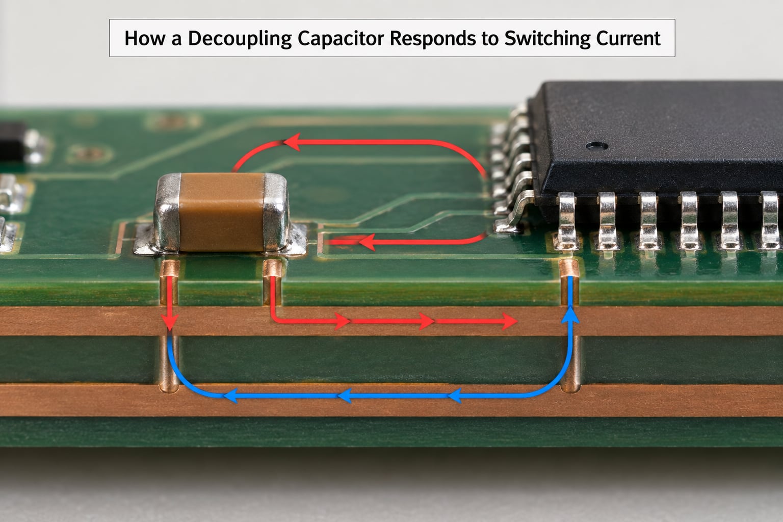
Watch what happens over a single clock edge. The internal transistors in the device go from drawing almost nothing to drawing a large current for a short window. Average current over the whole clock period looks modest, so the regulator never notices.
Charge leaves the plates of the nearby decoupling capacitor to feed that pulse. The capacitor discharges across the pin, and the supply-side voltage dips by an amount set by the loop inductance and the slope of the current. Meanwhile the capacitor’s own ESL resists the change, so the dip is not zero even with a perfectly placed part.
After the pulse ends, the recharge path matters just as much. Charge returns from the regulator and the plane through trace and via inductance, and that inductance can overshoot into ringing. A plane with a broken return path, or a cap whose ground pad relies on a thermal relief, turns that ringing into a damped oscillator that keeps ringing after the edge is over.
This is why two boards with identical schematic and BOM can behave completely differently. The difference is loop inductance, and loop inductance is a layout property, not a schematic property.
Decoupling Capacitor Types and Their Roles
Different frequency bands need different physics, so a single capacitor type never covers a rail from DC to a gigahertz. Most designs stack three tiers, and each tier exists for a specific reason.
| Type | Capacitance range | ESR and ESL | Where it earns its place |
|---|---|---|---|
| Multilayer ceramic (MLCC) | 1 nF to 100 uF | Very low ESL, low ESR, usable to hundreds of MHz | At the supply pin; the high-frequency tier |
| Aluminium electrolytic | 10 uF to thousands of uF | Moderate ESL, higher ESR | Bulk reservoir for slow load steps and inrush |
| Tantalum polymer or POSCAP | 10 uF to hundreds of uF | Lower ESR than electrolytic, moderate ESL | Bulk tier in the middle frequency range |
| Film | 1 nF to a few uF | Low ESR, low ESL, larger | Analog supplies and precision rails where ESR affects stability |
| On-die MIM or deep trench | Dense picofarad to nanofarad arrays | Lowest ESL, very small | Inside the package and on the die, for advanced nodes and chiplets |
The three capacitor types named most often are ceramic, electrolytic and film, and that taxonomy maps neatly onto the tiers: ceramic for high frequency, electrolytic for bulk, film where ESR and stability matter more than size.
How to Choose the Right Decoupling Capacitor
Start from the IC datasheet, not from a habit. Look for the recommended decoupling scheme, the maximum supply ripple the device tolerates, and the worst-case transient current the internals can generate.
Divide the allowed ripple by the transient current and you get a target impedance for the rail. That single number tells you what the power distribution network must present at every frequency the device cares about, and it is far more useful than picking a value out of a list.
Worked example: a device on a 1.0 V rail tolerating 50 mV of ripple while drawing 10 A in a transient. Target impedance is 50 mV divided by 10 A, which is 5 milliohms, and it has to hold across the whole switching spectrum. Multiply that requirement by the frequency range you must cover and you get the total capacitance you need once you account for each part’s own inductance.
Then work down the part list:
- Voltage rating. Pick at least double the rail voltage. Ceramic parts lose a large share of their rated capacitance under DC bias, and an X5R or X7R part can lose more than half its value close to its rating.
- Dielectric. X7R for general decoupling, C0G or NP0 where tolerance and temperature behaviour matter, such as reference or filtering nodes.
- Tolerance and ageing. Ceramics can start 10 to 20 percent off nominal and shift further over time, so design against the derated value.
- Package size. A physically smaller part has lower ESL and a higher self-resonant frequency, so it does the high-frequency work better.
- Quantity. Identical values in parallel reduce impedance while staying below the antiresonance problem. The goal is enough capacitance at the pin, not the largest nominal number you can fit.
Where to Place Decoupling Capacitors on a PCB
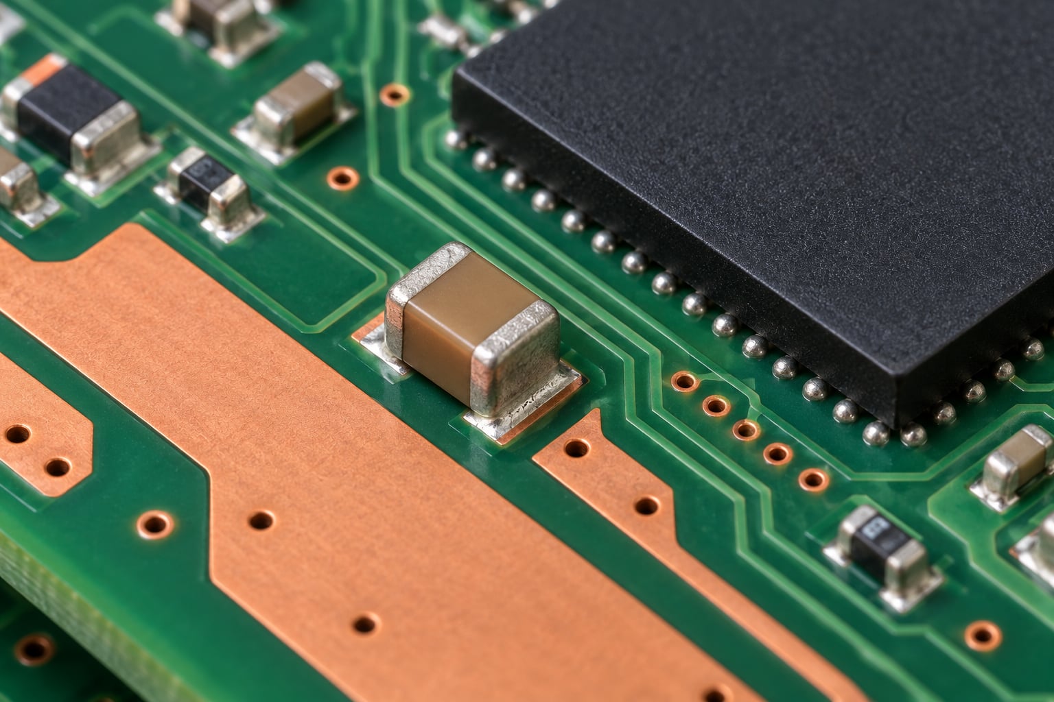
Place the capacitor as close to the power and ground pins as the package allows, on the same layer where possible, and give both pins the shortest, widest connection you can. Everything below follows from that one rule.
- Short and wide. A long thin trace behaves as an inductor. A 0201 part with a short connection usually beats an 0805 part across a long run.
- Solid ground. The ground connection needs a via right next to the capacitor ground pad. A thermal relief pattern under the pad adds inductance you did not draw.
- Pair the vias. If a via is unavoidable, use two, one for signal and one for the return, so the loop stays tight.
- Return path. The current loop must return through the plane or another conductor, not through a split in the plane.
- Split by size. Put the smallest capacitors nearest the pin and the bulk parts further away, so the bulk network does not dominate the high-frequency impedance.
- Interdigitate. Between ICs, alternate capacitor groups along the rail instead of clustering them at each end, which spreads the effective reach of the network.
- Decouple both ends. Put a capacitor at the supply source too, otherwise the loop between the source cap and the pin cap carries the transient.
Decoupling inside the package, on bumps or through silicon vias, is the same idea with less distance in it. The less inductance between the storage element and the core, the lower the impedance you can reach.
Common Decoupling Mistakes and How to Avoid Them
Stacking three values on every pin by habit. The classic set of 0.01 uF, 0.1 uF and 1 uF in parallel creates impedance peaks between the self-resonant frequencies of the values. Where two capacitors of different value sit in parallel, the small one’s capacitive reactance and the large one’s inductive reactance can cancel at some frequency, producing a peak where the network is more resistive than either part alone. Use values with a wide separation or identical values instead.
Assuming nominal capacitance is usable capacitance. This is the most common reason a decoupling capacitor appears to do nothing. An X5R part rated 10 uF can deliver a fraction of that on a 5 V rail at temperature.
Long traces and thermal relief. Both add inductance quietly. The schematic looks identical either way.
Relying on the bulk capacitor. A 470 uF electrolytic near the regulator does nothing for a 200 picosecond edge.
Relying on the ground plane alone. A plane is excellent, but a high-frequency current loop still needs a local, low-inductance return next to the pin.
Benchboarding a design that needs a PCB. Point-to-point wiring on a breadboard is mostly inductance, and a rail that works there can still droop on a board, or fail the other way around once the loop area shrinks.
Frequently Asked Questions
Where to put decoupling capacitors?
As close to the IC power and ground pins as physically possible, on the same layer where the package allows. Keep the trace short and wide, put a ground via right beside the capacitor ground pad, and avoid thermal relief patterns. Place the smallest values nearest the pin and bulk capacitance further away, so the high-frequency tier is not loaded down by the low-frequency parts.
What is bypass in electronics?
A bypass capacitor gives unwanted AC or high-frequency signals a low-impedance path to ground, while passing DC to the circuit it sits on. In practice bypass and decoupling describe the same physical part used at slightly different places: on a power rail it is decoupling, on a signal line, emitter or cathode it is bypassing. The distinction is about intent and location rather than a different component.
What is capacitor coupling?
A coupling capacitor passes an AC signal from one stage to the next while blocking the DC operating point of each stage, so the two stages can sit at different voltages. Decoupling does the opposite job: it keeps AC off a supply rail by shunting it to ground. One moves a signal along a chain, the other stops noise from getting onto a power line.
What are the three types of capacitors?
Ceramic capacitors give the highest capacitance in the smallest package with the lowest inductance, so they handle fast transients. Electrolytic capacitors offer far more capacitance for bulk storage, inrush and slow load changes. Film capacitors have low ESR, low leakage and predictable behaviour, which makes them the usual choice for precision analog supplies where stability matters more than size.
Why is 0.1 uF the most common decoupling value?
It is a compromise that happens to land in a useful band: small enough that a 0402 or 0201 package still has acceptable self-resonance, and large enough to supply a meaningful share of a switching transient. It is a starting point, not a rule. Derating under DC bias, the target impedance of your rail and the self-resonant frequency of the package all matter more than the nominal value.
Can too many decoupling capacitors cause problems?
Yes. Different values in parallel can resonate with each other and create an impedance peak between their self-resonant frequencies, where the network is less effective than either part alone. On boards with many pins, this shows up as noise concentrated at one frequency rather than broadband. Using identical values, or values with a wide separation, avoids the peak.
Conclusion: Start With the Supply-Impedance Requirement
Capacitors are used for decoupling because the path to the chip is inductive and the chip demands current faster than that path can supply it, and a capacitor is the only component whose impedance drops as frequency rises. Read the datasheet, turn the allowed ripple and the worst-case transient into a target impedance, then pick enough parts to hold that target across the band that matters.
Do the layout part with the same care as the selection. Put the smallest, lowest-inductance parts at the pin, keep the loop tight, and give the ground return a solid path. If you do those two things together, the reason for decoupling stops being a rule you were told to follow and becomes something you can see on a scope.