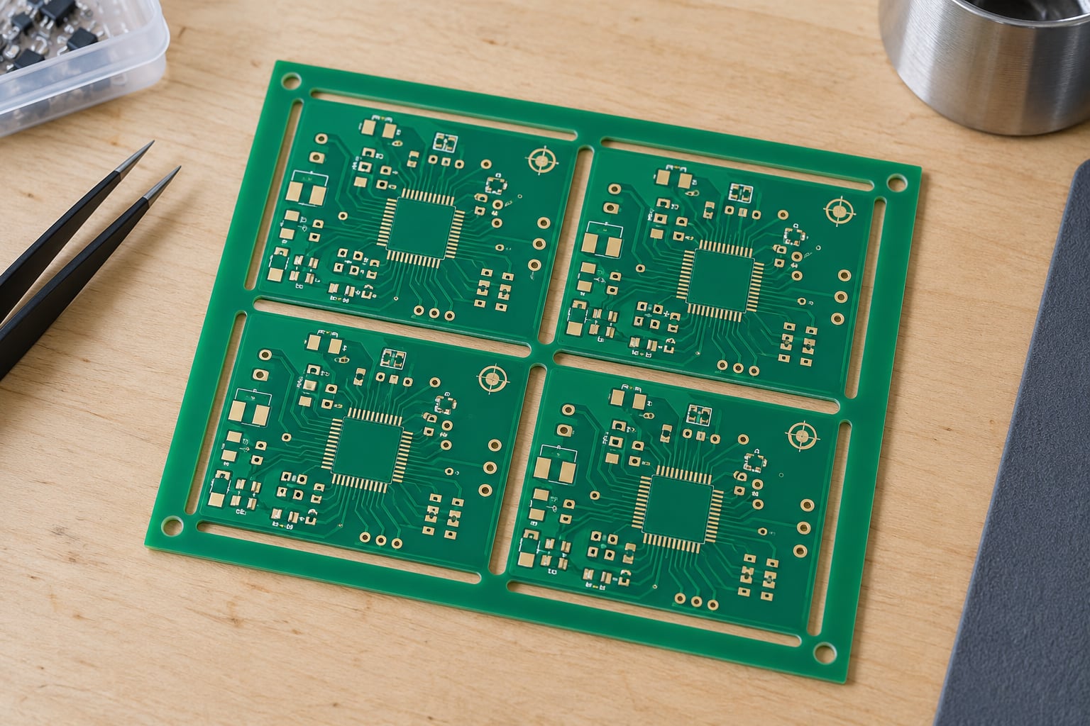
How to panelize a PCB? You copy your finished board into a step-and-repeat array on a larger carrier, connect the copies with routed tabs, V-score lines or perforated mouse bites, add rails, tooling holes and fiducials for the assembly line, then export the whole panel as new fabrication data. The order matters: get your fabricator’s panel rules before you touch the layout, not after. A whole panelization session takes an hour or two on a simple array, more once you’re checking clearances against a vendor PDF.
The payoff is real. Boards under roughly 50mm on a side are hard to place, hard to solder and easy to lose on a conveyor, so they get run as one rigid unit and separated at the end. Panelization typically cuts per-board manufacturing cost by 15-30% because material, setup and handling amortize across every copy on the panel.
Table of Contents
- What You Need Before You Panelize
- Step-by-Step: How to Panelize a PCB
- 1. Confirm the Fabrication Order Requirements
- 2. Choose a Panelization Method
- 3. Define the Panel and PCB Copies
- 4. Add Coupons, Rails, and Tool Holes
- 5. Create Fiducials and Machine Targets
- 6. How to Panelize a PCB Edge: Breakaway Paths
- 7. Run Design and Fabrication Checks
- 8. Export and Approve Fabrication Data
- Common Mistakes
- Frequently Asked Questions
- Should a PCB designer panelize the board before ordering?
- What is the most common PCB panelization method?
- How many fiducials does a PCB panel need?
- Can every PCB be safely duplicated in a fabrication panel?
- What files should I send with a panelized PCB?
- Conclusion
What You Need Before You Panelize
Panelization is a design-for-manufacture step, not a drawing trick. You need a specific set of inputs before you open your PCB editor, and most of them come from the fab rather than from you.
- Source board files — the schematic and board you have already DRC-cleaned, with all text converted to shapes and any filled zones re-poured.
- Fabrication drawings — the fab’s own outline, drill and layer notes, including which layers count as finished copper.
- Panelization guidelines — the vendor document that states panel size, permitted waste, breakaway method and any assembly constraints.
- Your PCB editor — KiCad, Altium, EasyEDA, Allegro or DipTrace. All of them can copy and paste a board into an array.
- CAM or panel preparation software — useful for adding process coupons, checking the panel against the fab’s drill file, or merging boards without a full CAD tool.
- Panel size limits — the largest panel the fabricator’s routing table, V-scoring saw or laser will accept.
- Allowable board-edge tolerances — how much material can sit between a routed edge and finished copper, which differs sharply between V-scoring and milling.
- Routing and breakout requirements — router bit diameter, the passage gap it needs between tools, and how many breakaways the fab will accept on one board.
- Assembler requirements — many SMT houses refuse V-cut panels, and they each have their own opinion on rail width, fiducial count and test-point placement.
- A named contact at the fab — the engineer who will answer a question the day before CAM upload.
Keep the fab’s PDF open in a second window while you work. Every number below is a typical industry value, and each one needs confirming against the specific shop that will cut the panel. IPC-2221 covers general design practice, but panel dimensions are always facility-specific.
Step-by-Step: How to Panelize a PCB
Eight steps, in this order. The manufacturer’s fabrication capabilities and design rules take priority over every generic panelization setting you might find in a tutorial or script.
1. Confirm the Fabrication Order Requirements
Before changing anything in your design, get the exact numbers your fab builds to. Ask for the board outline and finished dimensions, layer count, finished thickness, copper weight, surface finish, minimum line and space, drill tolerances, and the panelization method they prefer.
Also confirm permissible panel waste and any array constraints on their side. If the boards are going to be assembled, tell them that up front — several assemblers will not accept a V-cut panel at all, which pushes you toward mouse bites or routed tabs.
You are finished with this step when you can state the score depth, the tab width and the minimum copper-to-edge clearance in millimetres without guessing.
2. Choose a Panelization Method
Five methods cover almost everything, and they differ on board shape, edge finish, separation force and cost.
V-scoring cuts a V-shaped groove roughly one-third of the board thickness from each side, leaving a thin web that snaps cleanly by hand. It gives the smoothest edge and the best material yield, but it only works on straight, parallel board edges with a fairly uniform thickness — practical from about 1.0mm up. Groove angles are typically 30, 45 or 90 degrees.
Routed tabs leave small uncut bridges of laminate holding each board in place. Tabs are usually 2-5mm wide and snap off with fingers or light plier pressure, and this is the only method that handles irregular outlines, holes near edges and components that overhang the board. The tradeoff is a slightly rougher edge and more routing time, which is why a vendor quotes a different rate for tab-routed work.
Mouse bites are routed tabs drilled full of rows of small non-plated holes, typically 0.3-0.5mm diameter. The holes weaken the tab until it fractures along the perforation instead of tearing. They are cheap and fast to produce, but they stop working on thicker laminates, where the residual material will not snap cleanly, and they leave a ragged edge and visible residue.
Drill connections use a single line of holes between boards. Combination methods score some internal edges and route others, which is common when a panel mixes boards of different thickness.
Selection criteria in order: board thickness first, then whether any edge is routed or irregular, then how close components sit to the board edge, then board separation method, then whatever the fabricator’s equipment prefers.
3. Define the Panel and PCB Copies
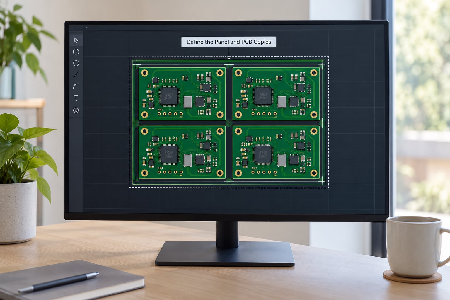
Panel dimensions, usable routing area and edge setbacks come from the fab, not from your CAD grid. Work out the usable area inside the panel edge, subtract the routing margin, then step-and-repeat the board from that boundary. Anyone learning how to panelize a PCB for the first time should confirm this arrangement with the manufacturer before drawing anything else on it.
In KiCad the practical route is File > Append Board (or Paste Board in older versions) inside an empty project. In Altium, PCB Panel Editor takes a board list and generates the array with its own source, destination, gap and rotation fields. Both let you paste the fabrication data rather than manually copying geometry by hand, which is where most array mistakes start.
Orientation matters for yield. A board rotated 90 degrees often fits more copies on the same panel, and for a non-rectangular outline the rotation can change the routing path entirely. Duplicated copies stay electrically identical unless you mirror them, and mirroring swaps the board to the bottom layer and flips the silkscreen, so only mirror when the design is genuinely two-sided and symmetric.
Panels are commonly ordered with a 100% multiplier for good boards and a lower percentage for test articles on the same sheet.
4. Add Coupons, Rails, and Tool Holes
A panel needs features your bare board never had. Process coupons sit in unused panel space and let the fab measure copper weight, etch, plating and surface finish after the build. Breakaway rails run around the array so a technician has something solid to grip, and for wave solder or conveyor work the rail width has to match the pallet or the 2-inch conveyor class the line uses.
Tooling or registration holes are non-plated through holes, typically 2.0-3.0mm diameter, that let the panel locate on the machine bed. They are not fiducials and they are not interchangeable with them. Ask the fab which of these it actually requires; some shops add their own frame and rails in CAM, and duplicated holes from both sides are a common cause of a rejected first article.
5. Create Fiducials and Machine Targets
Fiducials are copper targets that optical inspection and the placement machine use to align the panel, usually 1.0mm diameter pads with 2-3x their size in solder mask clearance. A panel normally carries asymmetric global fiducials — three marks in an L or asymmetric triangle, never identical or symmetrical — plus local fiducials on each board for fine correction.
Two rules catch people out. Repeating identical fiducials across the array confuses automated optical inspection, because the software cannot tell which is which. And placing a fiducial too close to a routed edge or a V-score line means the machine loses it as soon as the panel is broken down.
Use copper-only targets, not solder-mask-only ones, and check the drill file for any conflict with panel tooling holes. Test points and programming headers in the breakaway rails cost nothing in usable board area and can save a fixture later.
6. How to Panelize a PCB Edge: Breakaway Paths
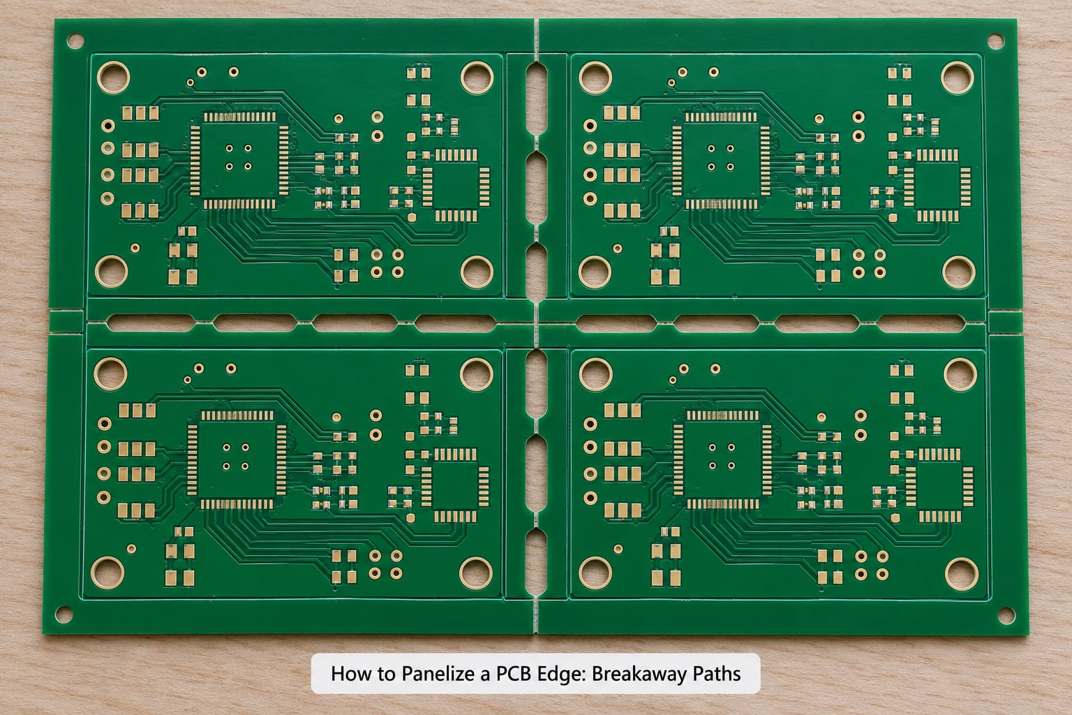
Breakaway paths are the geometry that holds the panel together, and their shape decides how the boards come apart. Routed slots separate the boards fully except at the tabs. V-score lines run straight across the board edge with no copper inside the groove. Mouse bites add drill rows inside the tab itself.
Check five things on every breakaway path. First, tool access: a router bit needs a passage gap, typically 2.0-2.54mm, and it cannot enter an edge narrower than its own diameter, which is why so many designs have to be redrawn before panelizing. Second, stress-sensitive components — anything within about 3mm of a breakaway, or any large ceramic capacitor sitting near the edge, is a crack risk. Third, exposed copper: keep finished copper back from a V-groove by about 1mm, or 20 mil, versus 5 mil when you are routing.
Fourth, board support. Every copy must be held flat by the panel during reflow, which means tabs close enough together that the board never sags on a hot conveyor. Fifth, the allowance: score and routing both remove material, so leave the kerf or scoring allowance in your spacing or the finished boards come out undersized.
Standard practice puts breakaway tabs 10-12mm from the board corner and spaces them 77mm centre-to-centre, with 100mm as a practical maximum on a long edge. Use the fabricator’s numbers when they differ.
7. Run Design and Fabrication Checks
Run your normal design rule check on the panel, not just on the single board. Then work through the panel-specific list, because most DRCs do not cover it.
- Duplicate or missing layers after the merge — a copy that brought its own solder mask or paste layer can silently override the panel’s.
- Net integrity, so renamed nets or duplicated copper pours did not merge across copies.
- Drill coordinates that still match the panel origin, and drill files exported for the panel rather than the source board.
- Board outline closure, with no stray edge lines from the original board left inside the array.
- Clearance from panel features to every routed edge and score line.
- Silkscreen clipping, since merged text and pasted labels often land outside their board.
- Component placement near breakaways, checked against your assembly house’s rules.
- Accidental connections between arrayed copies, which is the classic failure when mirroring.
The final CAM file still needs an independent review. Your CAM operator works from the exported data, not from your intention, so what they see is what you get.
8. Export and Approve Fabrication Data
Export Gerber or ODB++ from the panel, plus the drill file, and write a fabrication drawing for the panel that identifies the outline, the stackup, the finished thickness and the breakaway method. A separate panel drawing showing the array layout, board count and breakaway locations saves a phone call.
Include a layer map, the stackup information and any impedance requirements, plus a revision identifier that matches every other file in the package. Add assembly notes covering rails, fiducials, test points and the depanelization method you expect.
Before uploading, confirm the panel Gerber and drill files match the intended arrangement: open them in a viewer and count the board copies, check the first and last copy for clipped features, and verify the file revision against your drawing. Then send the whole package to your contact and wait for approval rather than placing the order the same hour.
Common Mistakes
These seven account for most panelization problems that come back from a fab.
Ignoring the fabricator’s rules. Generic tutorial defaults are not your fab’s defaults. Fix: treat the vendor panelization guideline as the specification and note every value it overrides.
Choosing a panel the equipment cannot route. A panel larger than the shop’s routing table or scoring saw is rejected outright. Fix: confirm maximum panel dimensions before you arrange anything, and check the usable area after routing margins.
Placing breakaways under components. V-score lines and tabs that run beneath a part, a connector or a crystal invite cracked terminations and lifted pads. Fix: keep parts roughly 3mm clear of any breakaway path, and move edge-mounted connectors inwards if you can.
Omitting asymmetric fiducials. Three identical global marks confuse optical alignment and cause placement drift across the panel. Fix: use an L or asymmetric triangle of global fiducials plus one local set per board, and never repeat an identical pattern.
Exporting incomplete drill data. Re-exporting drills from the source board instead of the panel gives you the right tool list against the wrong coordinates. Fix: export from the panel document and verify drill counts in a CAM viewer.
Assuming mirrored copies are identical. Mirroring flips layers, silkscreen text and any asymmetric footprint. Fix: mirror only when the design is symmetric, and check the bottom silkscreen reading correctly after the flip.
Confusing board-level and panel-level features. Fiducials and rails belong to the panel; board outlines and courtyards belong to each copy. Fix: label the two on your panel drawing so the fab does not remove features you need.
A few habits that pay off later. Run the DRC on the panel, not on the single board. Keep the source board untouched and panelize into a separate file, so you can regenerate the panel when the design changes without losing your master. Add test points in the rails while you have the space. Put a version marker on the panel outside any board, so a mixed sheet can still be identified after depanelization. And record which depanelization method the boards will be separated by: hand breaking suits V-score, a saw suits routed tabs, and a laser suits thick or multilayer work where mouse bites will not snap. 355nm UV and diode-pumped Nd:YAG are the common laser sources, and laser cutting needs an allowance for a slightly wider kerf than a router.
Frequently Asked Questions
Should a PCB designer panelize the board before ordering?
Only if the board is small or the assembler requires it. Most SMT lines, conveyors and pick-and-place machines struggle with boards under roughly 50mm on a side, so those are almost always panelized. For a larger standalone board, panelizing adds routing cost, waste and a depanelization step for no benefit. Confirm the requirement with your assembler before you commit.
What is the most common PCB panelization method?
Routed breakaway tabs are the most common, because they work on any board shape, thickness and layer count and tolerate components near the board edge. V-scoring is the most common on thin, rectangular boards where a smooth edge matters. Mouse bites sit in between as the cheapest option, but they fail on thick laminate and leave a rough edge.
How many fiducials does a PCB panel need?
A panel normally carries three asymmetric global fiducials, roughly 1.0mm copper targets with 2-3x solder mask clearance, plus one local set on each board copy for fine alignment. The global marks must not be identical or symmetric, because inspection software cannot resolve them. Confirm the count and placement with your assembler, since each line has its own expectations.
Can every PCB be safely duplicated in a fabrication panel?
No. Boards with tight or irregular edges can fail because the router bit cannot physically enter them, and boards with tall or edge-mounted components need breakaway paths moved clear of those parts. V-scoring also requires straight, parallel edges and a thickness of about 1.0mm or more. Check routability, edge clearance and thickness before you array, not after.
What files should I send with a panelized PCB?
Send panel Gerber or ODB++ data, the drill file, a fabrication drawing with the outline, stackup, finished thickness and breakaway method, and a panel drawing showing the array layout and board count. Add a layer map, impedance requirements, a revision identifier and any assembly notes covering rails, fiducials and test points. Wait for the fab’s approval before placing the order.
Conclusion
Start by getting your fabricator’s panelization guidelines and assembly requirements. Everything after that — the method, the array, the rails and fiducials, the breakaway paths, the checks and the CAM package — flows from those numbers.
Once the rules are in hand, how to panelize a PCB is a short, repeatable sequence: array the board copies, choose between routed tabs, V-score lines and mouse bites, add coupons, rails, tooling holes and asymmetric fiducials, run panel-level checks, then export and get approval. Do that once in a template and every later build becomes a number change rather than a redesign.