PCB thermal management is the practice of moving heat away from the parts on your board before it damages them. Almost every component you place converts some of its input power into heat, and if that heat has no low-resistance path out, junction temperature climbs until the part derates, drifts, or fails.
The basics are simpler than most guides make them sound. Calculate how much power each part dissipates, give that heat a copper path away from the pad, add vias when the path needs to reach another layer, and measure the result. Everything else is refinement.
Table of Contents
- What Is PCB Thermal Management and Why Does It Matter?
- Where the heat comes from
- What happens when a board gets too hot
- A comparison that makes the scale obvious
- How Do PCB Designers Spread Heat?
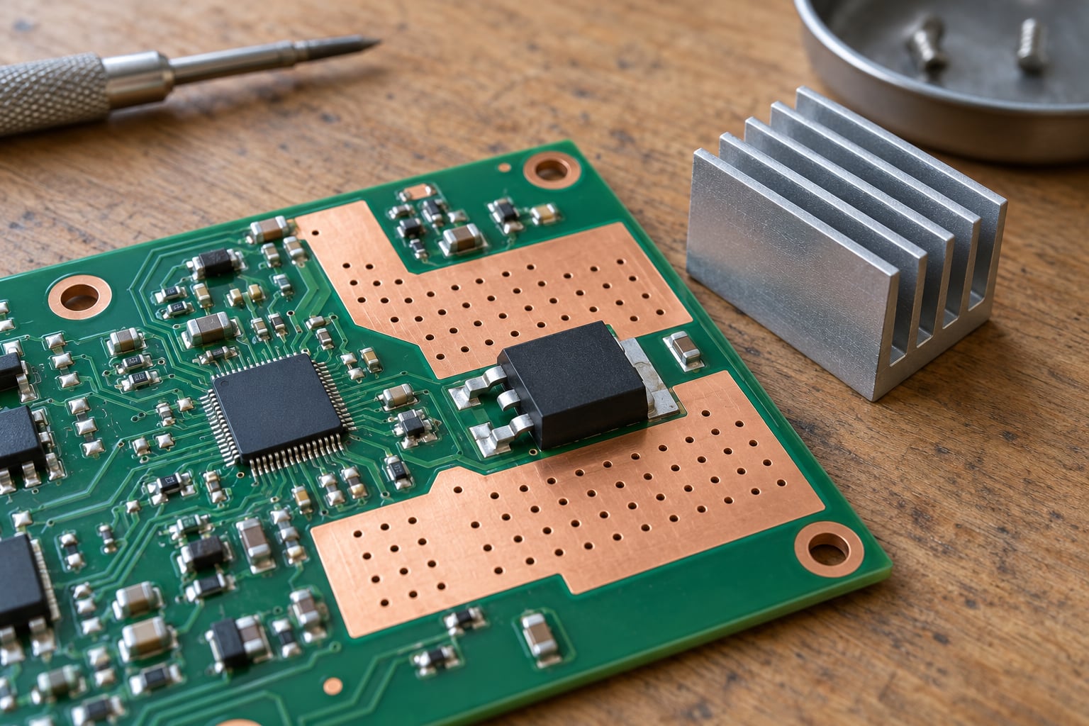
- Copper pours and planes
- Copper traces
- Thermal vias
- Thermal pads and exposed copper
- Heat sinks and thermal interface material
- Keepout and spacing
- How Do You Choose the Right Copper and Via Strategy?
- Via diameter and pitch
- Why more vias is not always better
- Solder wicking and the annular ring
- A worked example
- Which PCB Materials and Surfaces Help With Heat?
- Copper weight and layer count
- Dielectric thickness and surface finish
- How Do You Find Hotspots on a PCB?
- Pass one: calculate
- Pass two: inspect the layout
- Pass three: measure
- Component temperature limits to design against
- What Are the Most Common PCB Thermal Mistakes?
- 1. Thermal relief spokes under a thermal pad
- 2. Isolated hot components
- 3. Narrow thermal paths
- 4. Vias that do not reach useful copper
- 5. Denser vias than the pad allows
- 6. Heat sinks on an uninsulated pad
- 7. Blocked convection
- 8. Assuming copper alone can cool a high-power device
- How Can You Check a Thermal Design Before Fabrication?
- Frequently Asked Questions
- What is the formula for calculating heat dissipation?
- What are thermal vias in PCB?
- How do I calculate the thermal resistance of a heat pipe?
- How do I calculate heat dissipation of electrical equipment?
- Are copper pours always enough to cool a board?
- Should thermal vias be filled, and can they affect signal integrity?
- Conclusion: Start With the Hottest Component
What Is PCB Thermal Management and Why Does It Matter?

Heat leaves a component three ways, and all three are always happening at once. Conduction carries it into the package, the solder joint and the copper under it. Convection carries it off the board surface into the air. Radiation carries a smaller share into nearby surfaces and the enclosure.
On most boards, conduction into copper is the lever you control. That is why PCB thermal management basics start on the copper layer rather than in the case design.
Where the heat comes from
Passive parts are usually not the problem. A resistor loses a fraction of its rating, so a 0.25 W part rarely runs warm even at its full rating. Switching regulators, linear regulators, MOSFETs, power inductors, high-power LEDs and large processors are where the watts come from. Anything dissipating more than about 1 W deserves a thermal plan before layout, not after.
Producers and consumers also behave differently. A buck converter is a producer: heat flows out of the IC into the board. An output inductor or a series MOSFET in a converter is often a consumer, drawing heat in through its leads from copper that is already warm. Producers want copper under their own pad. Consumers want short, wide ties to the same warm copper, not an isolated pour of their own.
What happens when a board gets too hot
Every datasheet lists a maximum junction temperature, usually 125 °C to 150 °C. Exceed it and you get electromigration in the die and bond wires, faster aging of solder joints from thermal cycling, and shifts in parameters that can turn a working design into an unreliable one. Plastic packages soften, so a hot device also becomes a mechanical problem for whatever is clamping it.
Temperature also has a second-order effect that catches people out: performance depends on temperature. Regulators hold less accurately as they heat, sensors drift, and timing margins tighten on high-speed links. A board that meets its electrical spec at 25 °C can fail it at 70 °C.
A comparison that makes the scale obvious
A small sensor board with a low-power microcontroller and a few passives might dissipate well under a watt in total, spread over many square centimetres of copper. Temperature rise stays modest and no single part needs attention.
Now take a board with one regulator dissipating 4 W under a QFN package, or a processor with an exposed pad running at 15 W. The heat source is a few square millimetres, so the temperature at the die depends almost entirely on the thermal resistance of the path you gave it. That is a completely different design problem, and it is why the same layout habits do not work for both.
How Do PCB Designers Spread Heat?
There are seven tools most designers reach for, and each one trades something. Knowing what you give up is what separates a thermal design from a pile of copper.
Copper pours and planes
A solid copper pour next to or under a part acts as a heat spreader. It collects heat over a wide area and drops the local temperature gradient. The catch is diminishing returns: once the pour reaches roughly 25 mm on a side, the extra area stops helping much because heat has already spread as far as it can go before convection takes over.
Copper traces
A wide trace is a narrow pour. Use it to tie a producer to the nearest copper mass when a full pour will not fit. Keep it short, because every millimetre of length is added thermal resistance.
Thermal vias
A plated hole through the board carries heat from the top copper layer to an inner or bottom plane. FR-4 between layers is a poor conductor, so vias are how heat crosses a dielectric. They are the cheapest large-area heat mover available on a standard board.
Thermal pads and exposed copper
Open the solder mask under an exposed pad so the package can solder directly onto copper. That removes the thin polymer layer that would otherwise sit between die and copper, and polymer conducts heat poorly. The rule that catches beginners: do not put thermal relief spokes under a thermal pad. Spokes exist to control solder wetting on ordinary pads, and they cut the very path the pad needs.
Heat sinks and thermal interface material
A heat sink raises the surface area available to convection. The thermal interface material, or TIM, fills the microscopic air gaps between a flat package and a flat sink; air is a terrible conductor, so even a thin gap costs you degrees. Both are external to the board, which is why they come last after the internal paths are right.
Keepout and spacing
Space between hot parts lets convection do its job and stops adjacent packages from feeding each other. It costs board area, which is often the scarcest resource on a compact design.
How Do You Choose the Right Copper and Via Strategy?

The decision is simple in principle: connect the heat source to the largest amount of copper you can afford, and connect that copper through the dielectric with as many vias as the package allows. The details are where designs fail.
Via diameter and pitch
Engineers report 3×3 or 4×4 arrays of 0.3 mm vias on 1.0 mm pitch as a common starting point under a QFN pad. The pitch matters as much as the count, because it sets how much copper is left between holes to carry heat sideways. Typical fab rules run from 0.8 mm to 1.2 mm pitch with finished hole sizes around 0.2 mm to 0.5 mm; check your fabricator’s actual capability rather than assuming.
Why more vias is not always better
Below saturation, each extra via lowers the path resistance. Past saturation, the return flattens, and at very dense arrays performance can even get worse because the plating between closely spaced holes is thinner and conducts less well. That effect shows up in thermal simulation before it shows up on the bench, so model the array rather than counting holes.
Signal integrity is the other reason to stop. A solid wall of vias next to a controlled-impedance trace changes the impedance. Keep the array inside the pad footprint, or leave clearance to the trace field.
Solder wicking and the annular ring
A large unfilled hole under a pad pulls solder down through capillary action during reflow. You get a weak, dull joint on a part that expects a specific solder volume. Two fixes: keep holes at or below about 0.3 mm, or tent the holes with solder mask so solder cannot enter. Tenting costs you nothing thermally.
Also confirm the annular ring survives plating. Below the fabricator’s minimum, a plated thermal via is a reliability risk that outweighs its thermal benefit.
A worked example
Take a QFN buck regulator dissipating 3 W with an exposed pad and an RthetaJA of 28 °C/W in still air. The predicted rise is 3 W x 28 °C/W = 84 °C, so a 55 °C ambient gives a 139 °C case. That is past the limit before you even look at the die.
Connect the pad to a solid pour on the top layer, then drop a 4×4 array of 0.3 mm vias on 1.0 mm pitch into the nearest ground plane. Re-run the same estimate with the board-level resistance of the modified design, which will be materially lower than the package figure alone. If the new rise still does not fit the budget, the next moves in order are vias into a second plane, heavier copper, an exposed copper area, then a heat sink over the package with a TIM.
For a second worked example, the same 3 W part on a board with only a single 6 mm square pour and no vias will show a much larger local gradient than the array version, because heat has nowhere to travel horizontally before it hits still air. The pour size, not the part, sets the local temperature.
Which PCB Materials and Surfaces Help With Heat?
Substrate choice decides how much heat can move sideways, and copper weight decides how much can move at all. Material selection is the point where a thermal requirement starts costing real money, so it is worth being deliberate about the numbers.
| Material | Approx. thermal conductivity | Where it makes sense |
|---|---|---|
| Standard FR-4 | 0.2 to 0.3 W/m·K | Low and moderate power; vias handle the vertical transfer |
| High-Tg FR-4 | 0.3 W/m·K | Lead-free reflow and higher reliability, similar thermal behaviour |
| Aluminum core MCPCB | Roughly 150 to 200 W/m·K in the core | High-power LED, power converters, motor drivers |
| Copper core MCPCB | Far above aluminum in the core | Very high density power stages where core conductivity is the limit |
| Ceramic substrate | 20 to 200 W/m·K depending on family | Power modules, RF and high-reliability applications |
Two non-obvious points from this table. First, moving from FR-4 to a metal core is a step of several hundred in conductivity in the horizontal direction, which is why a metal-core board can handle a heat flux of around 2 W/cm2 that no via array on FR-4 would survive. That threshold is a useful trigger: when your calculated power density approaches it, stop adding vias and change material.
Second, high-Tg FR-4 is not a thermal upgrade. It improves dimensional stability and reliability at elevated reflow temperatures, and that reliability matters if the board also runs hot, but it does not move heat better than standard laminate.
Copper weight and layer count
Going from 1 oz to 2 oz copper roughly doubles the cross-sectional area available to carry heat and current in each layer, and thick copper lowers resistance in current-carrying paths as well. It raises cost on every layer and complicates fine-pitch etching, so it is usually reserved for power stages rather than applied to a whole board.
Adding layers helps only if you then connect to them. A four-layer board with no vias from the hot pad to the inner planes gives you more copper you are not using.
Dielectric thickness and surface finish
A thinner core between layers lowers thermal resistance and reduces the via length heat must travel. Surface finish matters less than people expect for a bare board, but exposed copper on the top surface adds both conduction area and a surface that can convect directly to air. Keep in mind that solder mask is a polymer with poor conductivity, so a large opening over bare copper is a real thermal improvement and not just cosmetic.
How Do You Find Hotspots on a PCB?
You find hotspots in two passes: a calculation pass before you build anything, and a measurement pass after you have hardware. Neither is optional, and the second one catches what the first one missed.
Pass one: calculate
Get per-part power dissipation from the datasheet at your actual operating point. For a linear regulator, power is the voltage dropped across it multiplied by the current through it: a 5 V to 3.3 V converter at 1 A dissipates 1.7 W regardless of the load being fed. Multiply by RthetaJA from the same datasheet to get the temperature rise above ambient, then add ambient and compare with maximum junction temperature.
Two cautions. RthetaJA is heavily board-dependent, and a datasheet figure measured on a specific test board is a weak predictor of your board. And for parts with an exposed pad, ask your distributor or the manufacturer for the EDA or RthetaJED values if you need a defensible number.
Pass two: inspect the layout
Before simulating, look at the board. Every part above roughly 1 W should have a trace or pour touching it. Every exposed pad should have a solid connection with no spokes. Every thermal via array should sit inside the pad footprint rather than beside it. This review catches most real problems faster than any tool.
Pass three: measure
An infrared camera is the fastest way to find relative hot spots across a board, but it lies about absolute values: emissivity, shiny solder and reflective surfaces all skew readings. Use it to find where heat concentrates, not to certify a number.
Thermocouples give absolute temperature when bonded reliably, at the cost of being point measurements. Attach them to the pad or exposed copper where the part datasheet defines the measurement point, and insulate so the reading reflects the part and not the room.
Then test conditions decide whether your answer means anything. Ambient temperature, airflow direction and velocity, enclosure material and orientation all change the result. A board mounted flat in a sealed metal box is a different design problem from the same board on vertical rails in a moving airflow. Power cycling matters too, because heat capacity hides steady-state problems until the board has soaked for tens of minutes.
Component temperature limits to design against
Rather than memorising numbers, use the datasheet rating for each part and derate from it. As working guides, most consumer silicon is rated to a 125 °C or 150 °C junction ceiling, most consumer ICs specify a 70 °C or 85 °C ambient operating range, electrolytic capacitors commonly quote 105 °C, and many plastic packages are limited by about 260 °C peak for reflow but far lower for continuous operation. Automotive and industrial parts carry wider ambient ranges and tighter derating curves. Design against the specific part, not the category.
What Are the Most Common PCB Thermal Mistakes?
These eight turn up again and again in design review, and each has a straightforward correction.
1. Thermal relief spokes under a thermal pad
Spokes reduce the copper-to-pad connection to thin fingers, which is the opposite of the intent. Correct it with a solid connection and vias placed so the pad cannot wick solder away from itself.
2. Isolated hot components
A part surrounded by keepout, with only its own pads to carry heat away, becomes its own hotspot. Correct it by tying the part to the nearest substantial copper mass.
3. Narrow thermal paths
A 0.25 mm trace from a 4 W device is not a thermal path. Correct it with a pour, or with wider copper and more layers tied together.
4. Vias that do not reach useful copper
An array that stops in an unused layer moves heat nowhere. Correct it by confirming where each via lands and connecting that plane to something with area.
5. Denser vias than the pad allows
Arrays crowded to the point of plating risk and signal integrity problems. Correct it by staying inside the pad footprint and honouring the fabricator’s minimum annular ring.
6. Heat sinks on an uninsulated pad
Soldering a heat sink directly to a live pad shorts it. Correct it with an electrically insulating TIM rated for the voltage, and verify its thermal rating, which is usually lower than its electrical one.
7. Blocked convection
A board in a sealed enclosure with no vents cannot shed what it absorbs. Correct it with openings, spacing, or by accepting the enclosure temperature as the design ambient.
8. Assuming copper alone can cool a high-power device
Once calculated power density approaches roughly 2 W/cm2, no FR-4 design with any via count will hold the temperature. Correct it by moving to a metal-core or ceramic substrate, or by removing heat externally with a heat sink or enclosure that doubles as one.
How Can You Check a Thermal Design Before Fabrication?
The cost of a thermal fix rises steeply once Gerbers are released, so a short review before that point pays for itself. Work through this sequence.
- List every part above about 1 W with its dissipation at worst-case operating point.
- Compute temperature rise for each, using datasheet thermal resistance, and compare against maximum junction temperature with margin.
- Trace the heat path from each hot pad in the layout file: confirm solid copper, confirm vias reach a plane with area.
- Check the calculated power density against the material you have chosen, and switch material if you are near the limit.
- Check current capacity separately from thermal capacity, since these are different limits on the same copper.
- Run your fabricator’s DFM review on the via arrays, annular rings, tenting and copper-to-edge clearances.
- Add thermal test points now, on the board, in the locations you will want to probe later.
- On the prototype, measure with a thermocouple at the worst case: highest ambient, enclosure closed, and steady state after soak.
- Record the results and the conditions next to the design files, so the next revision starts from measured data.
If step two leaves you without margin, resist the urge to add more vias. Work outward through the list instead: larger pour, second plane, thicker copper, metal core, then an external heat sink. Each step costs more than the last, so taking them in order means you stop as soon as the numbers fit.
Frequently Asked Questions
What is the formula for calculating heat dissipation?
Two formulas cover most PCB work. Power dissipation is P = V x I, so the voltage dropped across a part multiplied by the current through it gives the watts it turns into heat. Temperature rise is delta T = P x Rtheta, where Rtheta is the thermal resistance in degrees Celsius per watt from the part datasheet. Add ambient temperature to get the final junction or case temperature and compare it with the maximum rating.
What are thermal vias in PCB?
A thermal via is a plated hole placed under a component thermal pad to carry heat from the top copper layer to an inner or bottom plane. FR-4 between layers conducts heat poorly, so vias provide the vertical path that the laminate blocks. They are usually arrays of small holes, around 0.3 mm on a 1 mm pitch, tied to a solid copper connection rather than thermal relief spokes.
How do I calculate the thermal resistance of a heat pipe?
For a heat pipe or any simple conduction path, thermal resistance is the temperature difference across it divided by the heat flowing through it: Rtheta = delta T / P, in degrees Celsius per watt. For a homogeneous layer you can also use thickness divided by conductivity times area, R = t / (k x A). For a PCB design, the practical route is the component datasheet RthetaJA figure, adjusted by board construction and measured on a prototype.
How do I calculate heat dissipation of electrical equipment?
Start at the source. Multiply the voltage dropped across each part by the current through it to get watts of heat. Add up the total for the board, then decide where that heat goes: through conduction into copper and vias, through convection off surfaces and out of the enclosure, and through radiation to nearby parts. Compare the resulting temperature rise against the component limits in the worst case, not the typical one.
Are copper pours always enough to cool a board?
Only for low and moderate power. Copper pours spread heat sideways, and beyond roughly 25 mm on a side the extra area gives diminishing returns because heat has already spread as far as it can before convection takes over. Above about 2 W/cm2 of power density, a pour on FR-4 cannot hold the temperature no matter how large it gets, and you need vias, a metal-core substrate, or an external heat sink.
Should thermal vias be filled, and can they affect signal integrity?
Filing a via with conductive epoxy or copper paste lowers its thermal resistance further, typically cutting the path resistance substantially compared with an unfilled hole, at a per-hole fabrication premium. Fill type is specified under IPC-4761, so state the type you want rather than leaving it to the fabricator. Vias do affect signals when a dense array sits beside a controlled-impedance trace, because it changes the impedance, so keep the array inside the pad footprint or keep clearance.
Conclusion: Start With the Hottest Component
PCB thermal management basics reduce to two questions for each part: how much heat does it make, and where does that heat go. Answer both before you lay out the board and most thermal problems never appear.
Find the highest-power components, give each one a solid copper connection with the solder mask opened, add a via array when the heat needs to reach another layer, and keep pouring copper until your numbers fit. Check the result by measurement in a real enclosure, not on an open bench. And if the required power density is above what the laminate can carry, bring in your fabricator and a mechanical engineer early rather than at the prototype stage.