PCB trace width calculation comes down to two numbers: how much current the copper has to carry, and how many degrees hotter than ambient you are willing to let it run. The IPC-2221 empirical formula turns those two inputs into a required cross-sectional area of copper, and dividing that area by the copper thickness gives you the trace width in mils. Internal layers use a smaller constant than external ones, so the same current needs a noticeably wider trace buried inside the board.
That is the whole method, and it takes about a minute once you have the numbers. What takes longer is deciding which numbers are correct, because the temperature-rise budget is a design choice, the layer position changes the answer, and two online calculators that both claim IPC-2221 can disagree on the same inputs. The rest of this page works through the inputs, the arithmetic, and the places where the popular shortcuts go wrong.
Key takeaways
- PCB trace width calculation is two steps: compute the required copper area from current and allowable temperature rise, then divide by copper thickness times 1.378 mils per ounce.
- The layer constant is k = 0.048 on an external layer and k = 0.024 on an internal layer. Internal traces come out about 2.6 times wider for the same current and temperature rise.
- Width grows faster than current. Each decade of current needs roughly 24 times the copper area, which is why a 10 A rail is not ten times a 1 A rail.
- Voltage drop frequently overrides temperature rise on long runs. Calculate both and take the larger width.
- IPC-2221 is a DC heating model. High-speed and RF routing is governed by characteristic impedance under IPC-2141 and IPC-2223, not by current capacity.
Table of Contents
- What Does PCB Trace Width Calculation Determine?
- What Information Do You Need Before Calculating Trace Width?
- How to calculate PCB trace width for a signal net first
- How Is PCB Trace Width Calculation Explained Using IPC-2221?
- The two equations and what each variable means
- Choosing the allowable temperature rise instead of copying 10 C
- PCB Trace Width Calculation Example for a 2-A Power Trace
- How Do You Check Voltage Drop and Electrical Resistance?
- How Do PCB Layer Type and Copper Thickness Change the Answer?
- Trace width lookup table by current, copper weight and layer
- Converting mils, ounces and metric for non-US fabs
- When Must Trace Width Be Treated as a Signal or Impedance Problem?
- Which Manufacturing and Assembly Constraints Affect the Final Width?
- How Do You Choose a Conservative Final Trace Width?
- Frequently Asked Questions
- What is the formula for calculating PCB trace width?
- Which PCB trace width do I need for 20 amps with 1 oz copper?
- What is the standard trace width for PCBs?
- What is the 3W rule in PCB design?
- Why do internal layer traces need to be wider than external ones?
- When is IPC-2221 the wrong standard to use?
- Conclusion
What Does PCB Trace Width Calculation Determine?
Trace width calculation determines how much current a conductor can carry before the copper itself gets too hot, and in doing so it also fixes the voltage drop, the power burned in the trace, and whether the copper survives thermal cycling. Width is the one dimension of a trace you can change freely, so it is the main lever a designer pulls on a power net.
It decides five things at once. Current capacity is the headline number. Temperature rise follows from it, and with it the thermal margin you keep against the components and laminate nearby. Voltage drop and the power dissipated as heat in the conductor both fall as width rises. Mechanical strength and manufacturability are the quiet constraints: a trace wide enough to survive reflow, handling and assembly torque has to stay inside the fabricator’s line-width rules.
There is one more that catches people out. On a high-speed net, width sets characteristic impedance, because impedance is a function of trace width, dielectric thickness and distance to the reference plane. On that net, width is not a free variable at all – it is dictated by the stack-up.
So the answer to “what determines trace width” is not one number. It is the largest of several requirements: what the current demands thermally, what the voltage-drop budget demands electrically, what the impedance stack-up demands on signal nets, and what your fabricator can actually produce.
What Information Do You Need Before Calculating Trace Width?
Six inputs drive the IPC-2221 calculation. Gather them in this order, because each one narrows the next. Missing any of them is the most common reason a calculation comes out wrong.
| Parameter | Symbol | Typical value | How to choose it |
|---|---|---|---|
| Current | I | 1 to 30 A | Use continuous worst case, not average. Add startup, inrush and motor stall current on top. |
| Allowable temperature rise | dT | 10 to 30 degrees C | Your thermal budget above ambient. See the section on choosing it rather than copying a default. |
| Layer position | k | 0.048 external, 0.024 internal | External means copper on the board surface. Internal means sandwiched between planes with no airflow. |
| Copper thickness | t | 1 oz = 1.378 mil, 2 oz = 2.756 mil | Confirm what the fabricator actually ships, in ounces per square foot, not micrometres you assumed. |
| Trace length | L | 10 mm to 1 m | Not used by the thermal formula. Needed the moment you care about voltage drop. |
| Acceptable voltage drop | Vdrop | 1 to 5 percent of rail | Set it from what the load tolerates. For sensor and reference lines, use the absolute millivolt budget instead. |
Two more constraints belong on the same list even though they are not equation inputs: the impedance target if the net is high-speed, and the fabricator’s minimum and maximum line width. The minimum often overrides the electrical result outright on low-current nets, which is why a 6 mil signal trace stays 6 mil no matter what a calculator says.
How to calculate PCB trace width for a signal net first
For a signal net carrying under about 100 mA, skip the current calculation entirely. Set the width to your fabricator’s minimum line width, usually 3.5 to 6 mil, and spend the saved space on routing. Power nets are where the calculation earns its keep.
On a mixed-signal board I usually split the nets into two classes in the CAD tool: everything below roughly half an amp gets the minimum, and everything above gets a width computed per net. Forum threads on r/PCB and electronics.stackexchange follow the same line of thinking, with most people describing 6 to 10 mil signals and 20 to 100 mil or a copper pour for anything past about 1 A.
How Is PCB Trace Width Calculation Explained Using IPC-2221?
The formula for calculating PCB trace width is a two-step empirical method from IPC-2221. First it computes the required cross-sectional area of the conductor in square mils from the current and the allowable temperature rise, using the empirical constants k, b and c. Then it divides that area by the copper thickness in ounces times 1.378 mils per ounce to give the width. The constant k is 0.048 for an external layer and 0.024 for an internal layer, so a buried trace needs about 2.6 times the width for the same job.
Written out, the two equations are:
Area (mil²) = ( I / (k × dT^b) ) ^ (1/c)
Width (mil) = Area (mil²) / ( Thickness (oz) × 1.378 )
That is the complete method. Everything else in this guide is about choosing the inputs correctly and interpreting the result.
The two equations and what each variable means
I is current in amperes. dT is the allowable temperature rise above ambient in degrees Celsius, not an absolute temperature – a trace that may run 40 degrees hot in a 25 degree room uses dT = 15, not 40. That single mix-up is the most common error I see in submitted calculations.
k is the layer constant, 0.048 external and 0.024 internal. b is 0.44 and c is 0.725 for both. The width step needs the copper thickness expressed in ounces per square foot, where 1 oz equals 1.378 mil of foil height.
Note what is missing. There is no trace length in either equation, and no ambient temperature. The model assumes steady-state DC heating with convection to still air at roughly 25 degrees, and it says nothing about resistance, which is why the voltage-drop check is a separate step.
Choosing the allowable temperature rise instead of copying 10 C
Ten degrees is a convention, not a rule. The temperature-rise term enters the formula raised to the power 1/c, roughly 1.38, so the relationship is strongly non-linear: allowing 30 degrees instead of 20 gives a required area of about 56 percent, not 67 percent. You cannot scale a result from one temperature budget to another by eye.
Use 10 to 15 degrees for a rail feeding a heat-sensitive part, for a board in a sealed enclosure with no airflow, or for anything on a long-life reliability program where copper anneals slowly. Use 20 to 30 degrees for a board in a ventilated chassis, a net that can afford to be warm, or a space-constrained layer where a 12 mm trace will not route and 6 mm has to.
Different traces on the same board can justify different budgets. A 5 A motor rail and a 200 mA enable line do not belong in the same net class, and they should not share a temperature-rise assumption either. What you cannot do is accept a default without knowing whether the board it lands on has airflow around it.
PCB Trace Width Calculation Example for a 2-A Power Trace
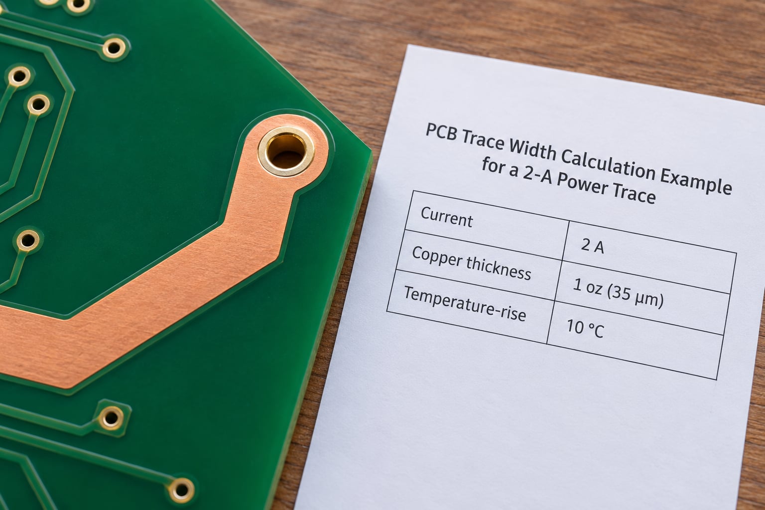
Here is the whole calculation for a common case: 2 A continuous, 1 oz copper, external layer, 20 degrees allowable rise, and we will check the voltage drop over a 100 mm run afterwards.
Step 1 – raise dT to the power b. dT = 20, b = 0.44, so 20^0.44 = 3.737.
Step 2 – multiply by k. The trace is on the outer surface, so k = 0.048. 0.048 × 3.737 = 0.1794.
Step 3 – divide current by that. 2 ÷ 0.1794 = 11.15.
Step 4 – raise to the power 1/c. 1 ÷ 0.725 = 1.379, so 11.15^1.379 = 27.8. That is the required cross-sectional area in square mils.
Step 5 – convert area to width. Copper is 1 oz, so the thickness term is 1 × 1.378 = 1.378. 27.8 ÷ 1.378 = 20.2 mil, which is 0.51 mm.
The same trace moved to an internal layer uses k = 0.024, which halves the denominator and multiplies the area by 2^1.379, or about 2.6. That gives 72.5 mil² and a width of 52.6 mil, or 1.34 mm. On 2 oz copper the width halves again, to 10.1 mil, because the area requirement does not change – only the thickness term does.
Twenty mil for a 2 A external rail matches the published IPC-2221 tables closely, which is a good sign the arithmetic is right. You will also see 30.8 mil quoted for the same 2 A if a calculator assumes a 10 degree rise. Both are correct answers to different questions, which is exactly why the temperature-rise assumption has to travel with the number.
Before drawing it, add your margin and round up to something the board can build. Rounding 20.2 mil to 25 mil costs nothing and covers etching tolerance, copper weight variation between fabricators, and a hot spot where the trace necks down to meet a pad.
How Do You Check Voltage Drop and Electrical Resistance?
IPC-2221 answers a thermal question. Once the trace is the right width thermally, you still need to know what it does to the voltage at the load, and for long runs that number is often the binding constraint.
Resistance comes from three values: the copper resistivity, the trace length and the cross-sectional area.
R = ( ρ × L / A ) × ( 1 + α × (T − 25) )
Vdrop = I × R
Ploss = I² × R
Copper resistivity at 20 degrees is 1.724 × 10^-8 ohm-metres, and the temperature coefficient is 0.00393 per degree, which is what the last bracket handles. Converted into a practical shortcut, 1 oz copper is about 0.49 milliohms per square, so a 1 inch long, 10 mil wide trace on 1 oz is roughly 49 milliohms. Resistance scales with length and inversely with width, which is the number to remember.
Back to the 2 A example on a 100 mm run. A 20.2 mil wide, 1 oz trace of that length works out to about 96 milliohms at room temperature, and a little more once the copper heats up. At 2 A that is roughly 192 millivolts dropped and 384 milliwatts dissipated in the conductor itself – a quarter of a watt baked into the board, sitting right next to your load.
This is where the two constraints collide. Doubling the width to 40 mil cuts the voltage drop in half but barely moves the thermal result, because the area equation is already satisfied. If the run is longer than about 150 mm, if the rail voltage is already low, or if the load is sensitive to a drooping supply, the electrical answer wins and you take the wider trace.
Forum users sizing battery packs and motor circuits hit this ordering constantly: the voltage-drop question arrives before the width question, and the two numbers need to sit side by side. The practical move is to check the budget first. If a 5 V rail can only lose 100 mV, the width that delivers that at 2 A over 100 mm is the width you draw, thermal results be damned.
How Do PCB Layer Type and Copper Thickness Change the Answer?
Two variables move the number more than anything else you can change in the schematic. Layer position changes the constant, and copper thickness divides the result directly.
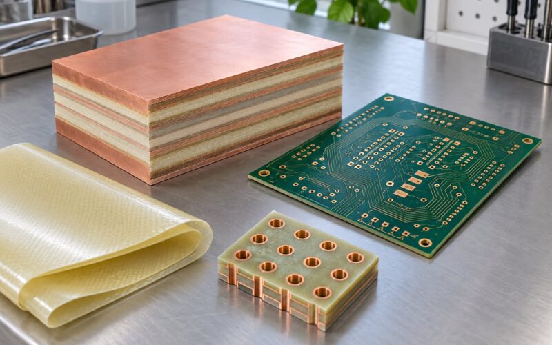
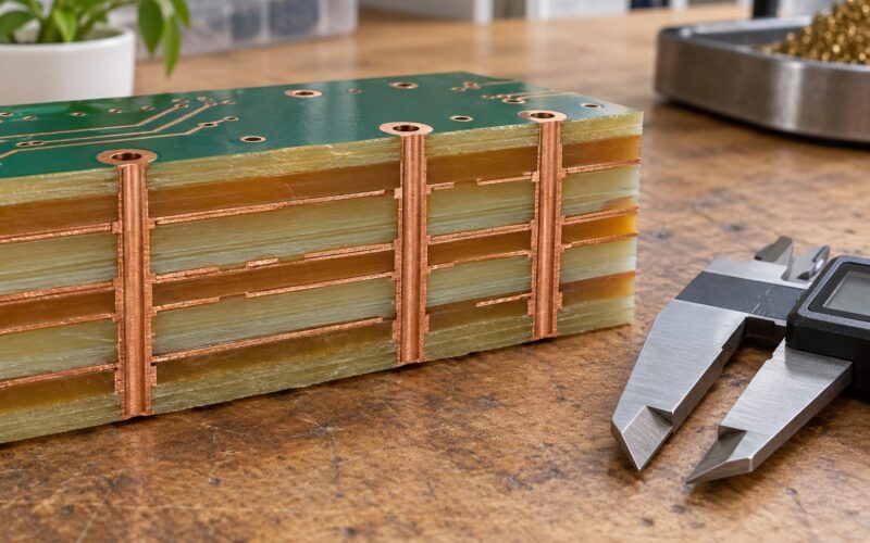
An external layer has copper on the surface, radiating to air on one side and to the laminate on the other. An internal layer is sandwiched between two planes with almost no convective path, so it sheds heat far more slowly, which is why its k value is exactly half and its required width is about 2.6 times larger. Copper thickness is a straight linear relationship: twice the foil, half the width for the same current.
Nearby copper changes things too. A wide trace running alongside a ground pour shares heat with it, so the isolated-trace result is slightly conservative. Thermal relief spokes and a fanout of thin segments are much worse than a solid run of copper, and a trace that necks down at a pad is only as good as its narrowest point.
Trace width lookup table by current, copper weight and layer
These are IPC-2221 results with the constants and equations above, rounded to one decimal place. Use them as a sanity check on your own arithmetic, not as a replacement for it.
| Current | 1 oz external, 10 C rise | 1 oz external, 20 C rise | 1 oz internal, 20 C rise | 2 oz external, 20 C rise |
|---|---|---|---|---|
| 1 A | 11.8 mil (0.30 mm) | 7.7 mil (0.20 mm) | 20.2 mil (0.51 mm) | 3.9 mil (0.10 mm) |
| 2 A | 30.8 mil (0.78 mm) | 20.2 mil (0.51 mm) | 52.6 mil (1.34 mm) | 10.1 mil (0.26 mm) |
| 3 A | 53.8 mil (1.37 mm) | 35.3 mil (0.90 mm) | 92.0 mil (2.34 mm) | 17.7 mil (0.45 mm) |
| 5 A | 109 mil (2.77 mm) | 71.4 mil (1.81 mm) | 186 mil (4.73 mm) | 35.7 mil (0.91 mm) |
| 10 A | 284 mil (7.21 mm) | 186 mil (4.72 mm) | 484 mil (12.3 mm) | 92.9 mil (2.36 mm) |
| 20 A | 736 mil (18.7 mm) | 483 mil (12.3 mm) | 1259 mil (32.0 mm) | 242 mil (6.14 mm) |
| 30 A | 1288 mil (32.7 mm) | 845 mil (21.5 mm) | 2202 mil (55.9 mm) | 423 mil (10.7 mm) |
Read the jump from 5 A to 10 A carefully: the external 1 oz trace at a 20 degree rise goes from 71.4 mil to 186 mil, not to 143 mil. That is the 1/c exponent at work, and it is why the common mental model of “double the current, double the width” fails so badly on power boards. The cells past about 10 A are also where the single-trace model stops being practical, and where a pour or a terminal block takes over.
Two cautions on the table. The model is valid up to roughly 3 oz of copper and a few tens of amps; beyond that the empirical basis thins out. And the figure that supposedly caps a PCB trace at about 30 A is a property of that model range, not a physical limit of copper – a busbar or a poured plane on 3 oz will go well past it.
Converting mils, ounces and metric for non-US fabs
Most non-US fabricators quote in millimetres and micrometres, so the conversion has to be exact. A mil is 0.001 inch, which is 25.4 micrometres or 0.0254 mm. That is a unit of length, nothing to do with solder mask or plating, despite what several calculators and blog posts claim.
| Copper weight | Mils of foil | Micrometres | Millimetres |
|---|---|---|---|
| 0.5 oz | 0.689 mil | 17.5 um | 0.0175 mm |
| 1 oz | 1.378 mil | 34.8 um | 0.0348 mm |
| 2 oz | 2.756 mil | 69.9 um | 0.0699 mm |
| 3 oz | 4.134 mil | 105 um | 0.105 mm |
Note the distinction the search results keep blurring: copper thickness is the height of the foil in ounces per square foot, trace width is the width of the conductor in mils or millimetres. They are independent inputs, and the formula uses thickness as a divisor, not as a synonym for width.
One more field reality. Cheap overseas fabricators ship 1 oz when the design assumed 2 oz, and nothing in the board says so. Ask for the copper weight in writing on the fab drawing, and record the width you calculated for the weight you actually specified.
When Must Trace Width Be Treated as a Signal or Impedance Problem?
On any net where edge rates matter, width is an impedance decision rather than a current decision. Above roughly a tenth of the critical frequency of your board, the trace behaves as a transmission line, and its characteristic impedance is set by width, dielectric thickness, distance to the reference plane and the continuity of that plane.
IPC-2221 has nothing to say about any of that. It models steady-state DC heating, so it will happily return a perfectly authoritative number for a 100 millivolt differential pair that is completely meaningless there. Copper skin effect at RF and GHz frequencies also means current does not fill the full cross-section, which is a different loss model again.
For those nets, the governing references are IPC-2141 for controlled impedance design and IPC-2223 for high-speed layout practice, together with your fabricator’s published stack-up. Where trace width and spacing are tight relative to the dielectric thickness, a 2D field solver gives a more honest answer than any closed-form approximation, and most fabricators will run one for you on request.
The practical rule: if the net carries meaningful current and needs controlled impedance, the two constraints are independent and both apply. A 50 ohm differential pair carrying 800 mA needs an impedance-controlled width from the stack-up and a thermal check on top, and the larger of the two geometric requirements wins.
Which Manufacturing and Assembly Constraints Affect the Final Width?
After the physics, the drawing rules take over, and on a dense board they frequently decide the outcome.
Minimum line width is the hard floor. Most fabricators run 3.5 to 6 mil trace and 6 to 8 mil spacing as standard capability, with 5 mil trace and 8 mil spacing common on cheaper processes. A calculated 4 mil result is not manufacturable there, and the net gets the fab minimum or a different copper weight.
Pad-to-trace transitions are the quiet failure. A 60 mil trace meeting a 40 mil pad has a 40 mil neck, and the neck carries the heat. Fillets, teardrops and short taper sections fix this. The same applies to via current sharing: two small vias side by side do not equal one large via, and a via barrel is usually the limiting element in a layer transition rather than the trace itself.
Annular ring, pad diameter and drill size are a separate calculation from trace width and get sized by different rules, even though forum users routinely ask about them together. A pad must keep its annular ring after plating and after the drill wanders, which is a mechanical requirement, not an electrical one.
Clearance between a hot trace and adjacent copper matters too. The 3W convention, where spacing between a high-voltage net and itself is three times the trace width, is an arc-flash mitigation convention for high-voltage nets, not a general clearance rule and not part of the current calculation. Solder mask adds a little thermal resistance, and a conformal coating or a thick surface finish changes the result slightly enough to matter on the hottest net.
Finally, nominal is not finished copper. A 10 mil drawn line may measure closer to 9.5 mil after etching, and outer layers lose thickness during processing while inner layers gain plating. That is exactly why the margin in the next section exists.
How Do You Choose a Conservative Final Trace Width?
The decision sequence is short, and running it in order is what separates a defensible number from a guess.
First, write down the six inputs: continuous current, ambient and maximum temperature, copper thickness, layer position, trace length, and the voltage-drop budget. Second, run the area and width equations with the layer constant for where the trace actually sits. Third, compute resistance and voltage drop over the real length, including the temperature correction.
Fourth, compare the two answers and take the larger. The thermal result and the electrical result are independent requirements, and a trace that fails either one fails. Fifth, add margin: round up to the next sensible increment and give yourself 20 to 30 percent on the thermal number for etching tolerance and copper weight variation. Sixth, check whether the net is impedance-controlled, and if it is, use the stack-up width. Seventh, send the final value to the fabricator with the copper weight and layer stated, and let their capability rules have the last word.
The mistakes that recur most often are worth listing plainly. Using average current instead of continuous worst case, and forgetting inrush. Using 40 degrees as dT when you meant a 40 degree absolute temperature. Applying an internal-layer result to an outer-layer trace, or the reverse, which silently halves or doubles your answer. Skipping the vias and thermal relief spokes in a high-current net. Sizing a two-inch run and applying the number to a twelve-inch run. And accepting a calculator result without knowing which constant it selected – the recurring complaint on r/PCB and electronics.stackexchange is two tools both claiming IPC-2221 returning different widths for identical inputs, which is almost always the layer constant or a skipped area step.
One circulating formula to distrust outright: W = k × I^0.44 / dT^0.725. It inverts the current and temperature exponents, drops the copper thickness entirely, and collapses the two-step area-then-width structure into one. If a page gives you that, the number it produces is not an IPC-2221 result no matter what the surrounding text claims.
Finally, if the calculated width will not fit, the trade-offs in order of preference are: thicker copper, a filled pour instead of a trace, a split plane with a narrower neck where the current is genuinely lower, accepting a higher temperature rise if the enclosure has airflow, and only then relocating components. On space-constrained boards the pour is the answer people actually use, and it is a good one – a poured region is simply a very wide trace with a much better thermal path.
Frequently Asked Questions
What is the formula for calculating PCB trace width?
IPC-2221 gives a two-step empirical formula. First, Area (mil²) = ( I / (k × dT^b) ) ^ (1/c), which converts current and allowable temperature rise into required copper area. Then, Width (mil) = Area (mil²) / ( Thickness (oz) × 1.378 ). The constants are k = 0.048 for an external layer and k = 0.024 for an internal layer, b = 0.44, c = 0.725. Copper thickness is entered in ounces per square foot.
Which PCB trace width do I need for 20 amps with 1 oz copper?
It depends on layer position and your temperature-rise budget, so never quote a single number. On an external layer with 1 oz copper, 20 A needs about 484 mil (12.3 mm) for a 20 degree rise, or 736 mil (18.7 mm) for a 10 degree rise. The same 20 A on an internal layer needs roughly 1259 mil (32.0 mm) at a 20 degree rise. At that level a poured copper plane is the realistic answer.
What is the standard trace width for PCBs?
Conventionally, signal traces run 6 to 10 mil, sub-amp power nets 20 to 40 mil, and 2 to 5 A nets 60 to 100 mil before you start using a lookup table. Those are starting conventions, not derived numbers. The real floor is your fabricator’s minimum line width, typically 3.5 to 6 mil trace and 6 to 8 mil spacing, which overrides the electrical calculation on low-current nets.
What is the 3W rule in PCB design?
The 3W rule is a spacing convention: where a high-voltage trace runs adjacent to itself or to a grounded conductor, keep the spacing at least three times the trace width, and add a grounded guard trace between them if you can. It is fault-current and arc-flash mitigation for high-voltage nets. It is not a general clearance rule, and it has nothing to do with calculating trace width for current carrying.
Why do internal layer traces need to be wider than external ones?
An internal layer is sandwiched between two planes, so it has almost no path to convect heat into air. The IPC-2221 constant reflects that: k is 0.048 on an external layer but 0.024 on an internal layer. Halving the constant multiplies the required area by 2^1.379, or about 2.6, so a 2 A 1 oz trace goes from 20.2 mil on the surface to 52.6 mil buried inside the stack-up.
When is IPC-2221 the wrong standard to use?
IPC-2221 is a DC heating model, so it is the wrong tool for high-speed and RF routing, where width is set by characteristic impedance against the stack-up rather than by current capacity. Use IPC-2141 for controlled impedance design and IPC-2223 for high-speed layout practice, and ask the fabricator to run a field solver where the trace width is small relative to the dielectric thickness. Copper skin effect also invalidates the model at RF frequencies.
Conclusion
Start by writing down six numbers: continuous current, allowable temperature rise, copper thickness, layer position, trace length, and the voltage-drop budget. Run the two IPC-2221 equations for the layer the trace actually occupies, check the resistance over the real length, and draw the wider of the two results plus a margin.
Then state the assumptions on the fabrication drawing, with the copper weight in ounces and the layer named, and have the fabricator confirm both against their current design rules. Every number that comes back to you later will be traceable to those six inputs.