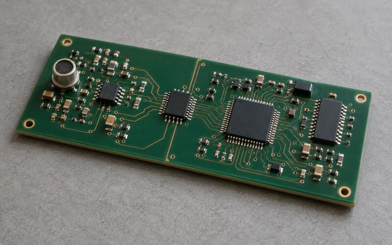
A chip datasheet is the manufacturer’s official description of an integrated circuit, and knowing how to read a chip datasheet is the difference between a circuit that works on the bench and one that ships. You don’t read it front to back. You confirm the exact part number, map the pins, check what the device can survive, check what it can actually do, then look at timing, application and package data in that order.
That order takes about 20 minutes on a microcontroller and about five on a small op-amp. What follows is the sequence I use, the tables that decide each step, and the specific numbers that quietly break designs when they’re misread.
A modern SoC datasheet can run past 400 pages. The five sections that decide whether your design works are the product brief, absolute maximum ratings, recommended operating conditions, the electrical characteristics table, and the pin description table. Everything else is detail you come back to when a specific question comes up.
Table of Contents
- What You Need
- Step-by-Step: How to Read a Chip Datasheet
- 1. How to Read a Chip Datasheet Front Page and Revision
- 2. Read the Pin Description and Pinout First
- 3. Check Absolute Maximum Ratings Carefully
- 4. Interpret Recommended Operating Conditions and Electrical Characteristics
- 5. Analyze Timing Diagrams and AC Parameters
- 6. Review Typical Application, Layout, and Package Information
- Common Mistakes
- 1. Treating typical values as guaranteed
- 2. Treating absolute maximum ratings as usable operating limits
- 3. Ignoring footnotes and test conditions
- 4. Reading a datasheet for the wrong part number or revision
- 5. Assuming the exposed pad is decorative
- 6. Trusting the current rating on page one
- 7. Copying the typical application circuit without checking your constraints
- 8. Skipping errata
- 9. Expecting bench measurements to match the datasheet exactly
- 10. Reading a datasheet for a part that is not yours
- Frequently Asked Questions
- What are the sections of a chip datasheet?
- How do I read a 400-page microcontroller datasheet?
- Should I design to the typical or maximum value?
- What is the difference between a datasheet and a reference manual?
- Is a replacement chip pin-to-pin compatible if the packages match?
- Why don’t my measurements match the datasheet values?
- Conclusion
What You Need
Before you interpret a single number, get the right documents open and know the conditions your board will actually run under. A datasheet is only meaningful against a supply voltage, a temperature range, a load and a package.
- The exact orderable part number. Not the marketing name. The full suffix matters: package type, temperature grade, pin count and sometimes a die revision.
- The datasheet at the newest revision. Check the document number and revision letter in the footer, and check the revision history table at the end for what changed.
- The document family. The datasheet covers electrical limits. Register descriptions, memory maps and peripheral behaviour live in a separate reference manual.
- The errata list. Documented silicon or documentation mistakes that the datasheet itself has not fixed.
- Hardware design guidelines or app notes for your specific use, if the vendor publishes them. These carry the layout and decoupling rules that decide EMI and thermal results.
- A land pattern library or the package drawing so you can match the footprint before you commit to the part.
- Your supply conditions. Nominal input voltage, tolerance, ripple, ambient temperature, expected load current and switching rate.
The document family trips up beginners because they assume one PDF holds everything. It usually does not.
| Document | What it answers | Where to find it |
|---|---|---|
| Datasheet | What this part can do within specified limits: features, ratings, electrical characteristics, timing, pinout, package, ordering codes | Vendor product page, distributor listings |
| Reference manual | How the part works: register map, bit fields, peripherals, memory, interrupt vectors | Vendor documentation page for the family |
| Hardware design guidelines | Layout, decoupling values, stack-up, and whether the evaluation board is the reference | Vendor application or design support site |
| Application notes | Worked circuits for one problem: a converter topology, a sensor interface, a specific bus | Vendor app note search, distributor app note hubs |
| Errata sheet | Known silicon or documentation errors and their workarounds | Vendor quality or documentation page |
| Package or footprint drawing | Land pattern, pin 1 orientation, courtyard, solder mask and paste apertures | Vendor mechanical drawings, IPC-7351 library |
If a vendor will not release the datasheet without an NDA, that is a signal, not an obstacle. It usually means the part is a custom or semi-custom ASIC, and the supplier may not support it once your order is done. Community reviewers on electronics forums treat gated documentation as a reason to look at a second source before committing.
Step-by-Step: How to Read a Chip Datasheet
1. How to Read a Chip Datasheet Front Page and Revision
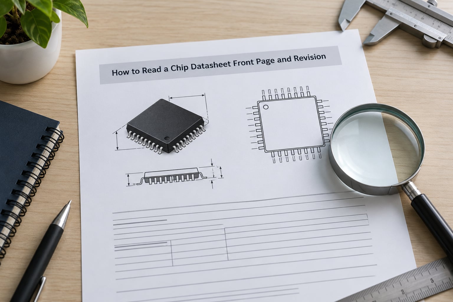
Start with the string you will actually order. A part number encodes package, temperature grade and sometimes a qualification level, and two parts differing by one suffix letter can have different pinouts or different supply limits.
Read the ordering information table at the back of the datasheet and match your suffix against it. It usually encodes package type, pin count, temperature range and shipping form. Then check the temperature grade: consumer parts commonly top out around 70 to 85 degrees C junction, industrial parts go to 105 or 125, and automotive-qualified parts carry an AEC-Q100 grade designation that has to appear in the ordering table.
Two more checks here. Lifecycle status tells you whether the part is active, not recommended for new designs (NRND) or obsolete. And the revision letter in the document footer plus the revision history table at the end tells you whether the document you’re reading has been corrected since it was first issued.
Working engineers treat the datasheet as a search engine rather than a book. Search the part number inside the PDF first, then read the table of contents to see how the vendor numbers its sections.
2. Read the Pin Description and Pinout First
The pin description table is the fastest way to find out whether the device does anything close to what you need. It tells you the pin number, the pin name, the direction, and the type for every pad on the package.
Learn the vocabulary quickly. A name with a bar over it, or any name ending in a slash or an overbar in the pin description, is active low, so it is asserted by pulling it low. Supply pins are named VDD, VCC, VIN or AVDD. Ground is VSS, GND or GNDA, and analog ground is usually a separate pin that joins single-pointed near the regulator. No-connect pins are marked NC and must be left unconnected unless the datasheet says otherwise.
| Pin name pattern | Function | What to check |
|---|---|---|
| VDD, VCC, VIN, AVDD, DVDD | Supply input | Voltage range, sequencing requirements, current per pin, decoupling value from the application section |
| VSS, GND, GNDA, DGND, AGND | Ground | Whether analog and digital ground are separate pins and how they must be joined |
| RESET, nRESET, EN, nEN | Reset or enable input | Active level, minimum assertion pulse width, required pull-up or pull-down, internal resistance |
| IN, OUT, D, Q, CLK, SCLK, SDA, SCL, TX, RX | Signal | Direction, voltage domain, whether it is multiplexed with a second function |
| NC | No connect | Leave floating unless the datasheet explicitly allows a tie |
| EP, PAD, TH, EXPOSED PAD | Exposed thermal pad | Tie to ground or supply, solder mask and paste aperture, via pattern, thermal via rules |
| TP, DNC, RESERVED | Test or reserved | No connect on a production board unless the vendor says otherwise |
Two details cause real hardware returns here. First, multiplexed pins: a single pad often does two jobs depending on a configuration register, so check the mode table before wiring. Second, the exposed pad on QFN and DFN packages. It is nearly always a ground connection and a heat path, and it needs its own solder mask opening and paste aperture in your land pattern.
When you print the pinout drawing, mark the pin 1 dot or chamfer and note whether the diagram is drawn as viewed from the top or from below. Drawings viewed from below invert left and right, which is a classic way to end up with a mirrored footprint.
3. Check Absolute Maximum Ratings Carefully
Absolute maximum ratings are stress limits. They describe the boundary beyond which the device can be damaged, and they are not operating targets. The table is short, appears early in almost every datasheet, and it is the single most misread table in the document.
The phrase “exceeding these ratings may result in permanent damage to the device” is doing heavy lifting. Exceeding an absolute maximum rating does not degrade performance or shorten life. It kills the part. Nothing in the datasheet promises survival above these values, even briefly, even at room temperature.
| Absolute Maximum Ratings | Recommended Operating Conditions | |
|---|---|---|
| What it describes | Instantaneous stress limits the device survives only without damage | Range over which the specified electrical characteristics are guaranteed |
| Typical entries | Supply voltage range, input voltage, output voltage, junction temperature, storage temperature, ESD withstand, power dissipation | Supply voltage, ambient or junction temperature, input and output levels, quiescent current limits |
| What happens outside it | Damage, or undefined behaviour the vendor will not warrant | Part may still work, but you get no guarantees on any parameter |
| Design rule | Never design here. Treat it as a fault-condition ceiling only | Design and test here, at both ends, with margin for supply tolerance and transients |
| Where you use it | Checking that your worst fault case, including a shorted output or a hot plug, stays inside a survivable bound | Every normal design decision: voltages, levels, currents, temperature |
The practical margin most designers use on supply voltage is modest for a well-regulated rail, but generous for anything that sees a hot-plug event, an inductive kick or a long cable. For a 3.3 V part with a 3.6 V absolute maximum, running a 3.6 V rail that occasionally touches 3.7 V during load transients is a design waiting to fail, and no amount of bench testing on a good power supply will reveal it.
4. Interpret Recommended Operating Conditions and Electrical Characteristics
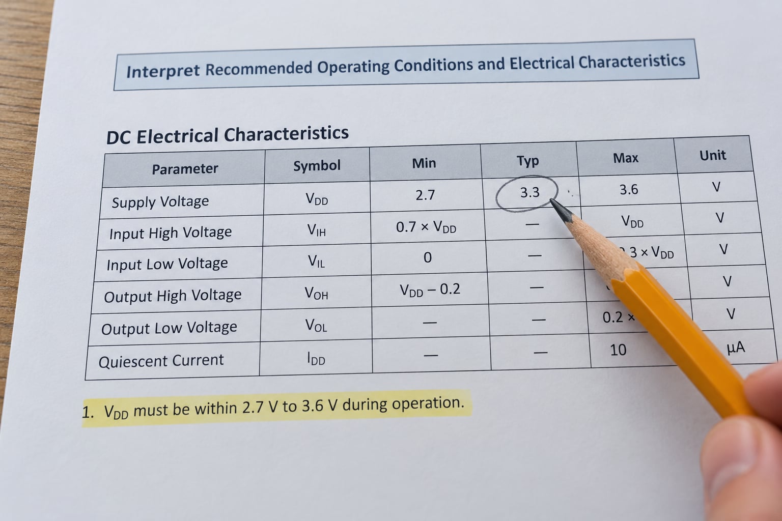
This is the table where designs are won or lost, and it uses three columns instead of one. Every row has a minimum, a typical and a maximum value, and the column headings carry footnotes that explain how each number was obtained.
| Column | What it means | What you design against |
|---|---|---|
| Minimum | Worst case the device still meets over all units, all specified conditions and the qualification sample. Usually a statistical limit, not an absolute physical bound | Yes. This is the guaranteed floor |
| Typical | The value most units produce, measured on a representative sample under one stated condition. Not a bound and not a promise | No. Use it only for estimating bias points, noise, offset and expected behaviour |
| Maximum | Worst case the device still meets under the same conditions | Yes. This is the guaranteed ceiling |
Design against minimum and maximum, and use typical only where you genuinely want the average behaviour, such as an internal reference that sets a divider ratio. Beginners routinely size a bias network or a comparator threshold from the typical column and then find the real part sitting outside their window at the temperature extremes. The classic forum complaint about typical values being off by an order of magnitude is correct: for many parameters the typical column has no guaranteed relationship to what you will receive.
Then read the test conditions, which sit in the column heading or a footnote. The same parameter often appears twice with different numbers because it was measured at a different supply voltage, temperature or load. A propagation delay measured at a 2.7 V supply into a light capacitive load is not the number you use for a 5 V rail driving a heavy load.
In the electrical characteristics table, the parameters that usually decide a design are the supply voltage range and its tolerance, input high and low threshold voltages, output high and low levels under stated load current, input leakage and output leakage, quiescent or supply current, output drive strength and the resulting logic levels, and power dissipation. For analog parts, add input offset voltage and drift, input bias current, common-mode rejection ratio, noise density, and the settling time or slew rate.
Check where those numbers are valid. Recommended operating conditions are stated over a temperature range, and many parameters are specified at 25 degrees C only. A parameter measured at 25 degrees C with a footnote saying “by design” or “parameters at 25 degrees C” is a typical-shaped number that many engineers misread as guaranteed.
One more thing worth reading on this page: the footnotes themselves. Footnotes carry the exceptions, the test method and the sampling basis, and they are where the real conditions hide.
5. Analyze Timing Diagrams and AC Parameters
Timing characteristics are where digital designs get subtle, because the datasheet usually gives a picture and the picture carries conditions that the number alone hides.
Setup time is how early a data bit must be valid before the clock edge that captures it. Hold time is how long it must stay valid after that edge. Propagation delay is how long an input change takes to appear at the output, and it comes as a minimum and a maximum, so it tells you both your shortest and longest path. Rise and fall times tell you how fast the output edge is, which sets how much crosstalk and ringing you can expect on a long trace. Maximum clock frequency tells you the fastest clock the part is guaranteed to handle.
Then check what the values assume. A memory datasheet timing table is often split by supply voltage and by I/O speed setting, with a separate column per combination. Read the driving load, the output capacitance and the supply voltage in the test conditions header. If your PCB has 20 pF of loading and the number was measured at 15 pF, you do not have a valid number.
A practical checklist for a synchronous design: confirm the clock frequency against the maximum frequency at your actual supply voltage; check setup and hold for every path into a register or FIFO; compute the longest path through sequential logic by adding propagation delay at the maximum value, not the typical one; and check the output timing for whatever the external device expects from you. For parts with an internal PLL or a prescaler, read the clock tree section rather than assuming the frequency you programmed into a divider.
If the part has an ADC, the timing section usually includes sample-and-hold time, acquisition time and conversion time, all usually specified at a particular clock divider and reference voltage. Check the ADC characteristics table separately for resolution, offset, gain error, integral and differential nonlinearity, and input impedance at the sample cap.
6. Review Typical Application, Layout, and Package Information
This is where specifications turn into a board you can build. The typical application circuit shows the vendor’s own working design: which capacitors go where, which pins get external components, and how the inputs are biased.
Pull the decoupling values from it rather than guessing. The application circuit usually shows a bulk capacitor plus one or more high-frequency capacitors directly across each supply pin, and the vendor’s recommended footprint fixes the via pattern. If the part has multiple supply domains, check for a power-up sequencing requirement; some parts need VDDIO before VDDCORE, and reversing the order can latch the device or damage internal ESD structures.
The mechanical drawings section gives the package outline, the pin pitch, the pin 1 marker, the exposed pad dimensions and the recommended land pattern. Match your PCB library footprint against that land pattern, not against a generic footprint with the same name, because pad dimensions and courtyard vary between vendors using the same package code.
Thermal data lives here too. Junction temperature, thermal resistance junction to ambient and junction to case, and power dissipation are usually listed together, and they are the numbers that connect the electrical table to your PCB. Thermal resistance assumes a specific copper area on a specific board layer count. Put a small package on a board with less copper than the datasheet assumed and the real junction temperature will be higher than your calculation, which is why designers rarely operate a regulator within 10 degrees C of its maximum junction temperature.
Which sections matter changes by device family, so search for the right ones rather than reading everything.
| Device family | Sections to read first | Parameters that decide the design |
|---|---|---|
| MCU or SoC | Product brief, pin description, recommended operating conditions, electrical characteristics, timing characteristics, memory map reference, clock tree, power sequencing | Supply voltage, I/O levels and drive strength, max clock per peripheral, ADC characteristics, quiescent current in each mode, package and pin count |
| Analog IC (amplifier, converter, reference) | Product brief, absolute maximum ratings, electrical characteristics, typical application, package | Supply range, offset and drift, bias current, noise, CMRR, bandwidth and slew rate, settling time, output drive, quiescent current, stability requirements |
| Power IC or DC-DC converter | Absolute maximum ratings, recommended operating conditions, electrical characteristics, typical application, thermal data, ordering information | Input and output voltage range, switch current limit, quiescent current, efficiency curve, switching frequency and ripple, thermal resistance, compensation guidance |
| MOSFET | Absolute maximum ratings, electrical characteristics at stated gate voltage and temperature, switching times, typical application, package | VDS, RDS(on) at the gate voltage you actually drive, VGS(th) spread, continuous drain current with derating, gate charge, SOA, body diode forward drop and reverse recovery, junction temperature |
| Diode and rectifier | Absolute maximum ratings, electrical characteristics, thermal data, package | Reverse voltage, forward voltage drop at a stated current, reverse recovery time, average rectified current and derating, junction temperature, package power dissipation |
The MOSFET row is where datasheet reading turns into real judgement. RDS(on) is specified at a gate voltage, usually 10 V, while a microcontroller port might only drive 3.3 V. Under that gate voltage the resistance can be substantially higher than the headline number, and comparing two parts quoted at different VGS tells you nothing. The same applies to the current rating, which assumes a case temperature far better than yours.
Finally, read the ordering information table again and record the orderable part numbers you will place on the bill of materials, and check for a land pattern or evaluation board reference to follow.
Common Mistakes
Most datasheet mistakes repeat across every discipline. Here they are, with the correction.
1. Treating typical values as guaranteed
Typical is the average of a sample under one stated condition. Design against minimum and maximum; use typical only for expected behaviour such as offset or noise estimates.
2. Treating absolute maximum ratings as usable operating limits
They are destruction limits. Design inside the recommended operating conditions and use the absolute maximum table only to confirm that fault conditions stay survivable.
3. Ignoring footnotes and test conditions
The footnote under a table changes the meaning of the number above it. Check the supply voltage, temperature and load each parameter was measured at before you use it.
4. Reading a datasheet for the wrong part number or revision
A suffix change can mean a different package, pin count or temperature grade. Match the full orderable part number and check the document revision history.
5. Assuming the exposed pad is decorative
On most QFN and DFN parts the exposed pad is a ground or supply connection and a heat path. Follow the land pattern for mask, paste and thermal vias.
6. Trusting the current rating on page one
Pin current limits, supply current limits and package power dissipation are different numbers, and the package limit assumes a case temperature you probably will not have. Derate against the thermal data.
7. Copying the typical application circuit without checking your constraints
The reference circuit assumes the vendor’s input range, output range and ambient temperature. If your input or your duty cycle is outside that, the compensation or the inductor or capacitor values change.
8. Skipping errata
Errata list known silicon and documentation bugs with their workarounds. A design that follows the datasheet exactly can still fail if a documented erratum applies to the revision you bought.
9. Expecting bench measurements to match the datasheet exactly
Real measurements differ because parts are derated, because PCB copper limits how much heat leaves the package, and because layout determines ringing and coupling. Treat the datasheet as the design contract and bench as reality check, not as an identity.
10. Reading a datasheet for a part that is not yours
Markings on a purchased part may be a lot code, not the part number. A datasheet for the wrong package or grade is worse than no datasheet.
The vocabulary behind these mistakes appears in a handful of qualifier words, and they are worth memorising because two of them are often swapped in the same document.
| Term | Meaning | How to treat it |
|---|---|---|
| Typical | The value most units produce under one stated test condition | Information only, never a design bound |
| Nominal | The named or target value, with no statistical meaning attached | A label, not a limit |
| Guaranteed | The value holds on every unit, over the full specified condition range, within the stated statistical basis | Design against it |
| Guaranteed by design | Not measured per unit on a production line, but the design margin and process controls make it hold | Reliable but not unit-tested; treat as guaranteed unless the vendor says otherwise |
| Warranted | The vendor commits to it, with remedies if it fails, often for a defined period | The strongest commitment a datasheet can make |
| Rated | A value the device is designed to withstand for a stated time under stated conditions | Read the duration and conditions, since “rated” hides both |
Frequently Asked Questions
What are the sections of a chip datasheet?
A chip datasheet usually runs in a near-standard order: product brief and features, pin description and configuration, absolute maximum ratings, recommended operating conditions, electrical characteristics, timing characteristics, block and application diagrams, typical application circuit, package and mechanical data, and ordering information. Large parts add memory maps, a clock tree and power-up sequencing. Reading those sections in that order gets you the design-critical facts fastest.
How do I read a 400-page microcontroller datasheet?
Page count is mostly register tables. You need about five sections: the product brief for what the part does, absolute maximum ratings, recommended operating conditions, the DC electrical characteristics table and the pin description table. Search the PDF for the parameter you need instead of reading sequentially, and pull the reference manual when you need register details. Print those five sections and annotate them by hand.
Should I design to the typical or maximum value?
Design to the guaranteed minimum and maximum, and use typical only where you want the expected value, such as estimating an offset or a noise figure. Typical describes what most units produce in a sample under one test condition, so it is not a bound. If your design only works at the typical value, it will fail on the units that sit at either limit, or outside the temperature range the test was run at.
What is the difference between a datasheet and a reference manual?
The datasheet describes what the part can do within specified limits: features, ratings, electrical and timing characteristics, pinout, package and ordering codes. The reference manual describes how it works: register maps, bit fields, peripherals, interrupt vectors and memory organisation. You need the datasheet to build the circuit and the reference manual to write the firmware or drive the peripheral correctly.
Is a replacement chip pin-to-pin compatible if the packages match?
No. Same package and same pin count is a starting point, not a guarantee. Check the pin description table name by name, the supply pin positions, the exposed pad connection, the input thresholds, the absolute maximum ratings and the timing numbers. Two parts can share a footprint and differ in pin function or voltage tolerance. Verify every pin before you approve a second source.
Why don’t my measurements match the datasheet values?
Datasheet values are guaranteed limits measured under stated test conditions, usually on a controlled bench with a specific load and temperature. Your board has different copper area, different layout-induced noise, different supply ripple and its own thermal environment, so real results differ. If the difference is small, that is normal. If a parameter is way off, check that the part is operating inside its recommended conditions and that you are not comparing against a typical column.
Conclusion
Knowing how to read a chip datasheet comes down to order and discipline. Confirm the exact orderable part number and the datasheet revision, map every pin from the pin description table, check the absolute maximum ratings so you know what would destroy the part, then design strictly inside the recommended operating conditions and the min, typ and max columns of the electrical characteristics table.
After that come timing, the typical application circuit, the land pattern and the thermal data. Start with the part number today, and the rest of the document stops being intimidating.