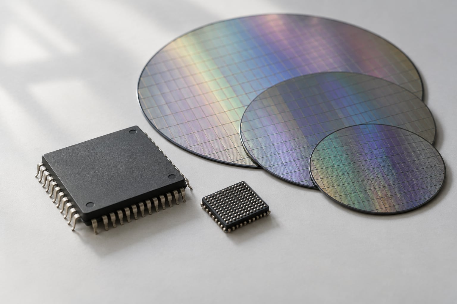
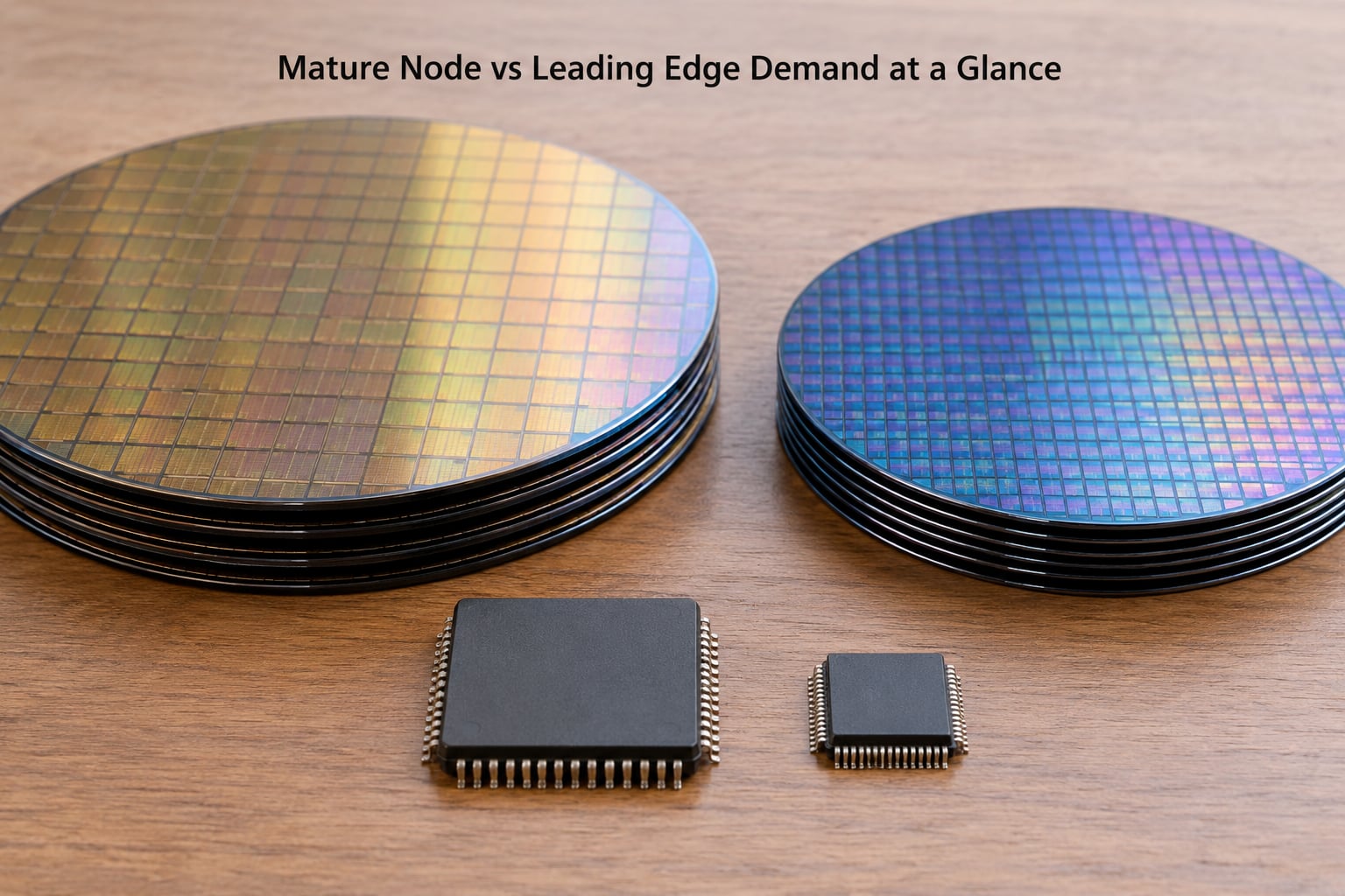
Mature node vs leading edge demand pulls in two opposite directions right now. Mature-node processes — 28nm and above — handle automotive, industrial, analog and power chips, and their capacity is tightening: SMIC reported Q3 utilization of 95.8% and Hua Hong Semiconductor reported 109.5%, while TSMC plans to retire some 8-inch lines by the end of 2027. Leading-edge processes — 3nm in volume, 2nm ramping — are effectively sold out to AI and hyperscaler customers, where the real bottleneck has moved to HBM and CoWoS packaging rather than wafers.
These are two different markets with two different clocks, and treating them as one market is the most common mistake in this discussion. A Reddit r/investing thread that ranks first for this query captures the confusion exactly: advanced nodes at TSMC are fully booked while older nodes still show slack, and nobody can say whether that pricing power holds.
The short version: mature-node demand is broad, fragmented and tied to the industrial and automotive inventory cycle. Leading-edge demand is narrow, contracted and tied to AI capital spending. Below is how each one actually works.
Table of Contents
- Mature Node vs Leading Edge Demand at a Glance
- How Do Mature Nodes and Leading Edges Differ?
- Mature Node vs Leading Edge Demand by Application
- What Drives Demand for Mature Nodes?
- What Drives Demand for Leading-Edge Nodes?
- How Capacity and Pricing Affect the Comparison
- Which Segment Is Growing Faster?
- Which Should You Choose?
- Frequently Asked Questions
- Are mature-node semiconductor demand and leading-edge demand competing with each other?
- Which applications create the most demand for mature-node wafers?
- Why is leading-edge demand so strongly influenced by AI chips?
- Does a smaller nanometer number always mean a better process?
- Should a chip designer choose a mature node for an AI product?
- Conclusion: Mature Demand Provides Scale, Leading Edge Creates Value
Mature Node vs Leading Edge Demand at a Glance
| Criterion | Mature nodes | Leading edge |
|---|---|---|
| Typical node range | 28nm, 40nm, 55nm, 65nm, 90nm, 130nm, 180nm | 7nm, 5nm, 3nm, 2nm |
| Process platforms | CMOS, BCD, eNVM, RF SOI | FinFET, then gate-all-around at 2nm |
| Primary end markets | Automotive, industrial, IoT, analog and power, consumer | AI accelerators, HPC, flagship smartphones |
| Who buys | Thousands of automotive, industrial and consumer customers | A handful of hyperscalers and accelerator vendors |
| Demand shape | Broad and fragmented, long tail of SKUs | Concentrated and largely pre-contracted |
| Design cost | Lower tapeout cost, reusable IP, stable PDKs | Very expensive mask sets, long design cycles |
| Product lifecycle | Frequently 10 years or longer | Often 2 to 4 years per generation |
| Pricing behaviour | Cyclical, sensitive to inventory corrections | Contracted, with visible pricing power |
| Binding constraint | 200mm and 300mm wafer capacity, analog and power line capacity | HBM supply and advanced packaging, not wafer starts |
| Current signal | Utilization at or above 95% at several foundries | Sold out through long-term agreements |
How Do Mature Nodes and Leading Edges Differ?
A mature node is any process that is no longer the technological frontier. In industry practice the line sits at 28nm and above, with 40nm, 55nm, 65nm, 130nm and 180nm forming the core band. Some analysts stretch the definition down to 22nm and 16nm, which matters more for sourcing decisions than for the label itself.
Leading edge means the newest node in volume production, which right now is 3nm, with 2nm ramping toward roughly 100,000 wafers per month projected by Q3 2026. These processes maximise transistor density and switching performance and pay for it with very high wafer costs and brutal design complexity.
Node names are not directly comparable across foundries. Two processes both labelled 7nm can differ meaningfully in density, power and cost, because each foundry names nodes for marketing reasons and uses its own design rules. A 28nm process at one supplier may not be interchangeable with a 28nm process at another without re-qualification.
SemiWiki forum discussion makes a related point worth remembering: TSMC’s 10nm was widely regarded as a weak node. Leading in technology and leading in volume are different things, and a process can be current without carrying much demand.
Mature Node vs Leading Edge Demand by Application
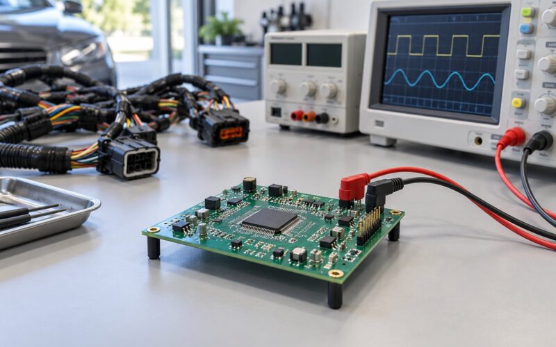
Automotive MCUs and body electronics sit almost entirely on mature nodes. ADAS and traction systems increasingly add leading-edge logic, but the dozens of small controllers around them do not need it. Power devices — power MOSFETs, rectifiers, gate drivers — run on 90nm to 180nm BCD platforms because breakdown voltage and on-resistance matter more than density.
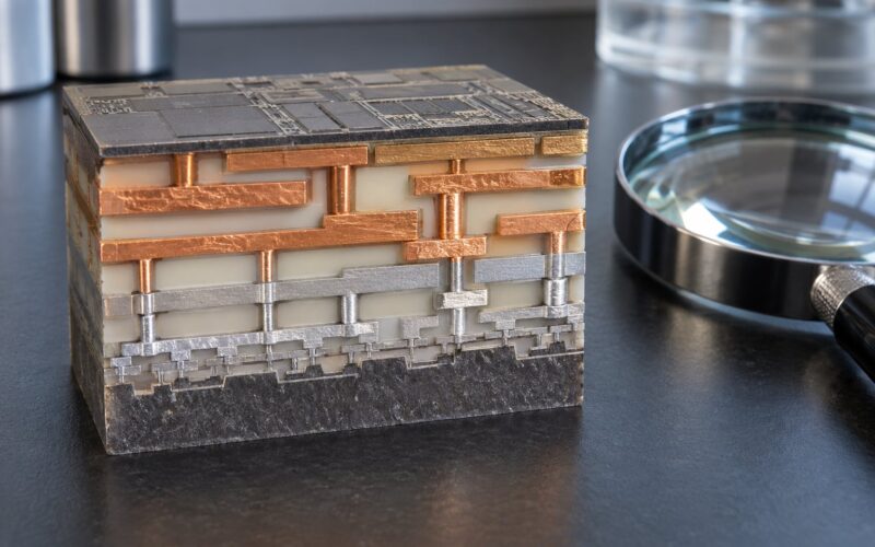
Analog and mixed-signal chips, PMICs and display drivers cluster on 55nm to 130nm. RF SOI for mobile and Wi-Fi front ends sits around 45nm to 90nm. CMOS image sensors use a mature logic node with a specialised imaging layer.
IoT components, industrial equipment controllers and consumer electronics are overwhelmingly mature-node products. Networking switches and infrastructure silicon are mixed: switching ASICs have moved to 5nm and 7nm, while the power management and connectivity companions on the same board stay at 55nm or above.
High-performance computing, flagship smartphones and AI accelerators are where leading-edge demand concentrates. So is the newest custom hyperscaler ASIC work. Everything adjacent to those parts is not.
What Drives Demand for Mature Nodes?
Long product lifecycles drive mature-node demand more than anything else. An automotive MCU approved for a platform stays in production for a decade or more, and the process it was qualified on must still exist in a decade. That single requirement anchors a large share of mature-node volume.
Low unit prices are the second driver. A power MOSFET that sells for cents cannot absorb the wafer cost of a 3nm process, so demand at the low end is structurally capped to mature platforms.
Broad SKU counts matter as much as volume. Thousands of part numbers ship in small quantities, which suits 200mm lines and specialty processes rather than cutting-edge capacity built for enormous volumes of identical products.
Automotive qualification cycles add friction that is easy to underestimate. AEC-Q100 qualification for the die plus an IATF 16949 audit of the supplier takes time, and re-sourcing a qualified part to a different node or foundry restarts much of it. That is why mature-node demand is sticky in both directions.
Industrial reliability and analog performance come next. Analog designers optimise for noise, offset and linearity over raw density, and years of characterisation on a stable PDK matter as much as any specification. Power management content keeps growing too, as every EV, industrial drive and solar inverter carries more power conversion than the one it replaced.
Current data supports the demand case. Global automotive semiconductor vendor revenue rose 6.5% year over year in 2025 to roughly 74.4 billion in sales, according to TechInsights. Lead times for analog, PMIC and power MOSFET parts have stretched to 12 to 30 weeks, which is a shortage signal rather than a soft-market one.
What Drives Demand for Leading-Edge Nodes?
AI training and inference dominate. AI accelerator revenue is growing above 55% annually and could pass 100 billion in annual sales by 2029. Each accelerator generation needs more compute per watt, more memory bandwidth and more transistors in a fixed power envelope, and only leading-edge logic delivers that.
Custom hyperscaler ASICs follow the same logic for the same reasons. In-house accelerators for inference and networking bypass the general-purpose route for cost reasons, and they still target 5nm and 3nm.
Energy efficiency is the quieter driver. Data centre power and cooling budgets are what push inference workloads onto newer processes, so performance per watt matters as much as raw throughput.
Advanced smartphones still anchor consumer-side leading-edge demand, and faster networking silicon keeps moving down. Both need the combination of density and low leakage that advanced processes provide.
Here is the twist that catches people: wafer capacity is no longer the binding constraint on AI silicon. HBM supply is projected near 488,000 die in 2026 with volumes growing about 37% year over year, and CoWoS-style advanced packaging capacity is the real gate. Multiple analysts and forum participants now argue packaging and assembly, not wafer fabs, are the true bottleneck.
Cost per transistor is also no longer falling on the classic curve. At 2nm, mask sets and yield ramps are expensive enough that the packaging and memory around the die can cost more than the die itself. That is a structural change from the last two decades.
How Capacity and Pricing Affect the Comparison
Leading-edge capacity is allocated through long-term agreements, so pricing is negotiated rather than posted. When TSMC’s advanced lines are sold out, the marginal wafer price is set by contract renewal, not by a spot market.
Mature-node capacity has tightened for structural reasons, not just demand ones. SMIC raised prices on some capacity by roughly 10% and guided full-year revenue above 9 billion in sales with gross margin of 18 to 20%. Analog Devices issued an across-the-board increase of roughly 15% effective February 1, 2026. Both actions are easier to interpret as supply discipline than as runaway demand.
TSMC’s plan to shut some 8-inch lines by the end of 2027 removes capacity from a market already running hot. That is a structural mature-node supply event, not a pricing story, and most coverage has framed it as the latter.
Regional capacity is uneven. TSMC’s 2nm ramps in Taiwan, Samsung builds in Korea, TSMC Fab 21 adds in Arizona, and SMIC plus Hua Hong add in mainland China with China-led 7nm capacity projected near 35,000 wafers per month by 2026. India’s programmes target 28nm to 65nm, with the Semicon India Programme at Rs 76,000 crore and ten India Semiconductor Mission projects across six states at Rs 1.6 lakh crore. Export controls shape which of that capacity each customer can actually buy.
For designers, the practical cost is the migration. Re-sourcing a qualified part to another foundry or node means new mask costs, new characterisation data and new customer qualification. For long-lifecycle parts, that often outweighs any per-wafer saving.
Which Segment Is Growing Faster?
Leading edge is growing faster in dollars today, and that is the honest answer. AI accelerator revenue growth above 55% annually and TSMC’s 2nm ramp to roughly 100,000 wafers per month by Q3 2026 are the visible numbers. Mature-node demand is recovering rather than booming.
But growth rate and durability are different questions. Leading-edge growth is concentrated in a handful of buyers making concentrated capex commitments, which makes it powerful and exposed at the same time. A pause in hyperscaler spending hits it immediately.
Mature-node demand is tied to the automotive and industrial inventory cycle, which turned up after a long digestion phase. Its risk is the mirror image: if EV and industrial orders disappoint, a second correction could follow. The 95.8% and 109.5% utilization figures could reflect a restocking blip as easily as a structural shift, and that is the bull-bear tension the top-ranking Reddit post raised.
Most analysts read advanced-node demand as structural and mature-node demand as cyclical-but-improving. India and China capacity additions will add mature-node supply over time, which argues for pricing pressure on commodity mature parts even as specialty capacity stays tight.
Which Should You Choose?
Choose the process your product requires, not the newest one available. The node is a consequence of the specification, and treating it as a marketing decision is how schedules get missed.
Fabless designers: start from lifetime volume, power envelope and required performance. Under roughly a few million units a year with modest compute, a mature or specialty node usually wins on total cost. Reserve leading edge for workloads where performance per watt is the product.
For anything shipping more than seven years, weight supply longevity above wafer price. Confirm the foundry commits to the node for the life of the program and that the PDK stays supported. A node that disappears mid-lifecycle is an expensive problem.
Foundries and capacity planners: note that the two demand pools are not substitutes. Adding 2nm does nothing for an automotive MCU, and retiring an 8-inch line does nothing for an AI accelerator. Plan each pool against its own end-market cycle.
EDA and IP suppliers: both segments need support, for different reasons. Leading-edge customers need advanced node sign-off flows, power and reliability analysis, and packaging co-design. Mature-node customers need longevity commitments, stable PDKs and analog and mixed-signal libraries that stay qualified for a decade.
Students and analysts: watch utilization rates, mask set announcements, packaging capacity and qualification announcements. Those four signals tell you more about node demand than any roadmap slide.
Frequently Asked Questions
Are mature-node semiconductor demand and leading-edge demand competing with each other?
No. They serve largely different customers and different cycles. Leading-edge capacity serves a small number of hyperscalers and accelerator vendors under long-term agreements, while mature-node capacity serves thousands of automotive, industrial and consumer buyers. Capacity added at one does not relieve the other, which is why both can be tight simultaneously.
Which applications create the most demand for mature-node wafers?
Automotive microcontrollers and power devices, analog and mixed-signal chips, power management ICs, display drivers, RF SOI front ends, CMOS image sensors and industrial control logic. These share long product lifecycles, low unit prices and qualification requirements that keep them on 40nm to 180nm platforms even as leading-edge processes improve.
Why is leading-edge demand so strongly influenced by AI chips?
AI training and inference demand needs maximum compute per watt, and only the newest processes deliver it inside tight data centre power budgets. AI accelerator revenue is growing above 55% annually and could exceed 100 billion in annual sales by 2029, so a single end market absorbs most advanced capacity and effectively sells it out.
Does a smaller nanometer number always mean a better process?
No. Node names are marketing labels and are not comparable across foundries. Two processes both called 7nm can differ in density, power and cost. Evaluate a process on yield, design rule maturity, available IP and total cost per good die rather than on the number attached to it.
Should a chip designer choose a mature node for an AI product?
Only for the supporting silicon. Power management, connectivity and control logic around an AI accelerator usually sit on 55nm to 130nm and can benefit from mature-node stability and cost. The accelerator itself, and any inference logic where performance per watt defines the product, belongs on a leading-edge process.
Conclusion: Mature Demand Provides Scale, Leading Edge Creates Value
Mature node vs leading edge demand is a question of two markets, not one market with two ends. Mature nodes deliver breadth: thousands of customers, decade-long lifecycles, and the analog, power and control silicon that every advanced product still depends on. Leading edge delivers value concentration: scarce capacity, contracted pricing, and the compute that AI workloads require.
Start by naming your requirements: performance, power, lifetime volume, qualification standard and supported lifecycle. The node follows from that list, and it is usually further along than instinct suggests.