Building a new semiconductor fab typically costs between 2 billion and 25 billion US dollars per facility, and leading-edge projects now run past 28 billion. Mature-node and specialty fabs land at the low end, advanced logic and DRAM fabs in the middle, and 2nm-class capacity at the top. Those are typical US planning ranges, not quotes: they shift by region, node and how much capacity you are buying.
The reason the range is so wide comes down to two variables that headline announcements rarely separate. The process node decides which generation of tools you need, and the monthly wafer capacity decides how many of them.
This guide maps nodes to capital cost, itemizes where the money actually goes, and shows how the headline number a company announces gets built up. Cost data as of October 2026.
Table of Contents
- How Much a New Chip Fab Costs to Build: Typical Ranges
- What Determines the Total Fab Cost
- What the Capital Is Actually Spent On
- How Much a New Chip Fab Costs Beyond the Building
- What Affects the Price
- How Leading-Edge Fabs Differ From Mature-Node Fabs
- What That Capital Does to the Cost of a Wafer
- Ways to Save
- Frequently Asked Questions
- How much does a small semiconductor pilot fab cost?
- Why do chip fabs cost billions when the factory building does not?
- What is the cheapest process technology for a new semiconductor fab?
- How much more does a leading-edge fab cost than a mature-node fab?
- How long does it take to build and qualify a new chip fab?
- Can a chip company reduce fab costs by buying used semiconductor equipment?
- Conclusion
How Much a New Chip Fab Costs to Build: Typical Ranges
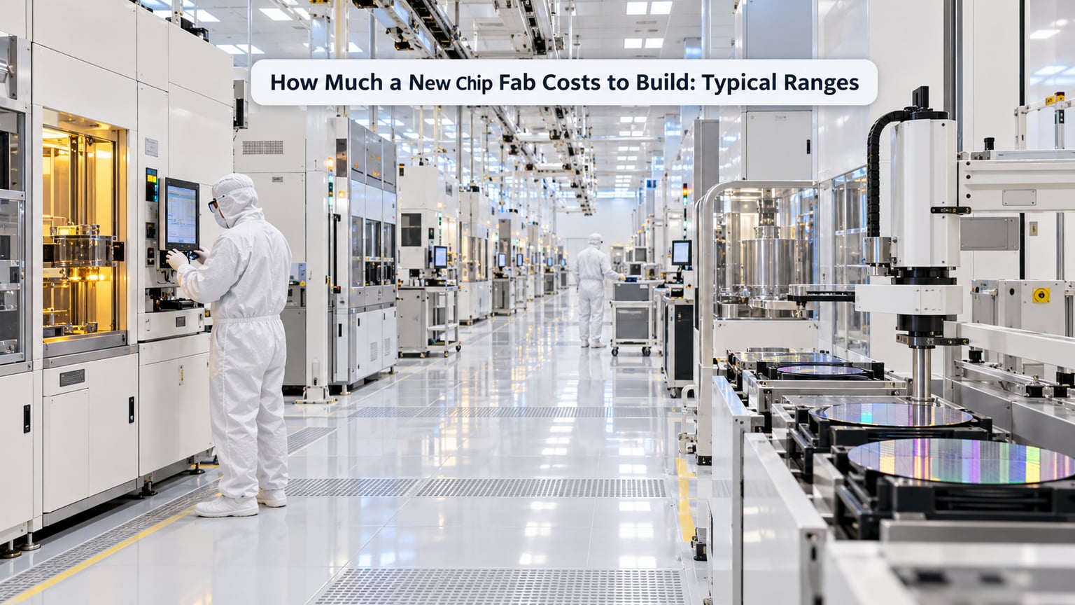
Start with the clearest anchors the industry has. JPMorgan has been widely reported as estimating that a 2nm fab running at 100,000 wafer starts per month costs upwards of 28 billion US dollars to construct, and a separate analyst estimate puts a 50,000 wafer-starts-per-month 2nm fab in the United States at roughly the same 28 billion figure over about 38 months of construction.
Those two numbers sitting at the same total for double the capacity is the single most useful thing to understand about fab economics. Capacity, not just node, sets the price tag, and it is the variable most often omitted from a cost conversation.
SEMI’s 300mm Fab Outlook, in its 3Q25 edition, put global 300mm fab equipment spending at 374 billion US dollars between 2026 and 2028. That equipment line alone dwarfs the construction budgets most people picture when they say “factory.”
Here is how the ranges break down by project type. Every figure is a planning range, and only the 2nm rows are anchored to a named published estimate.
| Project type | Typical process | Wafer capacity (WSPM) | Equipment intensity | Typical capital range (USD) |
|---|---|---|---|---|
| R&D or pilot line | Any node, DUV-based | 100 to 2,000 | Low: a small tool set, no volume redundancy | 0.1 to 1 billion |
| Mature-node MCU, analog and power | 65nm to 180nm, 200mm and 300mm | 20,000 to 50,000 | Moderate: mature DUV, long tool life | 1 to 3 billion |
| Specialty: SiC, compound semiconductor | 150mm and 200mm compound | 5,000 to 20,000 | Moderate, with heavier abatement needs | 0.5 to 1.5 billion |
| Memory, DRAM and NAND | 1b-class and finer, 300mm | 30,000 to 60,000 | High: heavy etch and deposition layering | 8 to 15 billion |
| Advanced logic, 7nm to 3nm | EUV lithography, 300mm | 40,000 to 80,000 | Very high: multiple EUV layers per device | 15 to 28 billion |
| Leading edge, 2nm and beyond | EUV with gate-all-around transistors | 50,000 to 100,000 | Highest: High-NA EUV and very tight overlay | 28 to 40 billion, with high-NA variants cited up to 100 billion |
For context on the top of that range, a widely shared industry estimate has a 1.4nm fab with High-NA EUV reaching as high as 100 billion US dollars. Treat that as a ceiling scenario rather than a typical project, but it shows where the cost curve is heading.
Real projects give those ranges something to sit against. Every number below is the announced or reported value for that specific project, and the scopes differ, so read the scope column before comparing anything.
| Project | Owner | Location | Announced value (USD) | Scope of the number |
|---|---|---|---|---|
| Arizona program, six fabs | TSMC | Phoenix, Arizona | 165 billion, 2nm production not until 2029 | Multi-fab program including supporting facilities |
| Arizona first fab | TSMC | Phoenix, Arizona | 12 billion construction; project up to 35 billion | Shell and construction versus full project scope |
| US expansion commitment | Samsung | Taylor, Texas | 73 billion committed | Multi-site US program |
| Clay campus | Micron | Clay, New York | 100 billion, the largest single US chip project | Long-term campus, including memory fabs |
| Terafab | Tesla / SpaceX / xAI | Austin, Texas | 20 to 25 billion announced March 2026; 10 GW power need | 2 million sq ft R&D phase one, 2nm ambition |
| India first fab | Tata and Powerchip | India | 910 billion rupees, about 11 billion | Single fab project cost |
The low end deserves more attention than it gets. A 200mm silicon carbide line for automotive traction inverters or a 200mm analog line for industrial power management is a few hundred million to a few billion dollars, not tens of billions. Yokogawa’s Minimal Fab concept, aimed at smaller-volume specialty production, explicitly targets cutting the investment required by a conventional fab down to a fraction of the total. A discussion in r/ECE put a single 14nm line at roughly 100 to 150 million US dollars, which is a useful order-of-magnitude anchor for anyone asking about a modest line rather than a leading-edge campus.
What Determines the Total Fab Cost
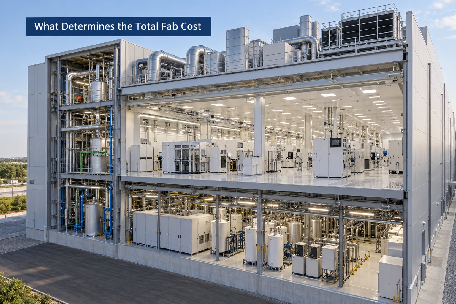
Roughly two-thirds of a fab’s capital cost is the wafer fab equipment itself: lithography, etch, deposition, chemical mechanical planarization and metrology tools bought from ASML, Applied Materials, Lam Research and TEL. The remaining third splits between the cleanroom building and its fit-out, utility and site infrastructure, and engineering, permits and startup costs.
That split surprises people who picture a fab as a large industrial shed. A fabrication plant is a chemical plant, a vibration-controlled laboratory and one of the biggest single electricity users on any industrial site, all of it sitting inside a cleanroom.
What the Capital Is Actually Spent On
Here is the breakdown, expressed as the share of total project capital that each category typically accounts for. The ranges are wide because a mature-node line and a 2nm line with the same building footprint allocate capital very differently.
| Capital category | Share of total project cost | What it covers |
|---|---|---|
| Wafer fab equipment (WFE) | 60 to 70 percent | Lithography, etch, deposition, CMP, metrology, track and probe tools |
| Cleanroom shell and build-out | 8 to 15 percent | Structure, raised floor, ISO-class envelope, air handlers, vibration isolation, tool move paths |
| Utility and site infrastructure | 5 to 12 percent | Dedicated substation, ultra-pure water, bulk gases, chemical abatement, wastewater treatment, make-up air |
| Site, land and permits | 2 to 5 percent | Land, grading, roads, environmental permitting, zoning approvals |
| Installation, qualification and engineering | 3 to 8 percent | Tool install, process transfer, mask sets, qualification wafers, engineering headcount |
| Startup and contingency | 5 to 12 percent | Initial materials, training, schedule acceleration, overrun reserve |
Two things in that table explain most of the surprises in a headline number. First, the WFE share is large enough that a tool delivery delay does not pause the project, it reorders it and adds cost. Second, site and permitting look trivial as a percentage, but on a multi-year schedule a permit that takes an extra year is the single largest schedule risk in the list.
How Much a New Chip Fab Costs Beyond the Building
This is where most confusion happens, and it comes from three different numbers being reported for the same project. Construction cost covers the shell and the cleanroom build-out. Project cost adds the tools, the utility infrastructure and startup spending. Company-reported capital expenditure is often broader still, covering several fabs, a packaging line and multi-year land purchases.
TSMC’s first Arizona fab is the clean example. Construction is reported at about 12 billion US dollars, while the broader project figure is quoted at up to 35 billion. The whole Arizona program across six fabs has been reported at 165 billion, with 2nm production not expected until 2029. None of those numbers contradict each other, because each covers a different scope. When you compare two fabs, match the scopes or the comparison is meaningless.
It helps to think about three distinct endpoints. A shell-only project gives you a grade-A cleanroom building with no process tools installed, which is roughly a fifth to a sixth of the eventual number. An equipped production fab means the building, utilities, tools and qualification are complete but nothing has been shipped. A fully operational high-volume fab adds working capital for raw materials, initial mask sets, engineering headcount and the yield ramp, and the cash position needed to absorb a poor first few quarters.
Only the third of those produces a chip anyone can buy. Marketing that difference is how a 12 billion construction figure and a 35 billion project figure end up describing the same building.
What Affects the Price
Process node and lithography generation. Each node shrink requires a new generation of tools with tighter overlay and smaller features, and the process step count rises as layers stack. Going from 7nm to 2nm roughly triples the capital per wafer relative to a mature node, and that gap widens at every node. The number that moves fastest is the exposure layer count, because every added layer means more patterning, more deposition and more metrology.
Fab size and monthly wafer capacity. This is the cost driver most often ignored. Tools, cleanroom bays and utility skids scale roughly linearly at first, so doubling wafer capacity in one building is usually cheaper than building two fabs. Some systems, though, are step-fixed: a substation, an abatement plant and a bulk gas farm are sized for the whole site, which is why the second fab on a campus usually costs less per wafer than the first.
Technology type. Logic, DRAM, NAND, analog, power, MCU and compound semiconductor fabs share a building type but almost nothing else. Memory fabs spend heavily on etch and deposition because the structures are deeply layered and vertical. Analog and power fabs tolerate older lithography but need heavier wet chemistry and chemical abatement. Compound semiconductor lines are smaller and rely more on specialist tool sets.
Tool set and cleanroom specification. ISO Class 1 lithography areas with vibration isolation and ammeter-class power quality cost more to build per square foot than a Class 7 assembly space, and a fab with multiple lithography generations needs separate bays with different environmental specs rather than one uniform cleanroom.
Location and incentives. This is the biggest reason a US or European fab costs more than a Taiwanese or Korean one. Land, power, permitting, union or trade-labor agreements, and local content rules all push cost up. The counterweight is the incentive package. For its Taylor, Texas project, Samsung’s local commitments were reported at a 30-year tax increment financing district valued at 467.8 million US dollars, 172 million from Williamson County, 314 million from the Taylor Independent School District, 27 million through the Texas Economic Development and Tourism Office and 200 million for roads. That is a serious offset, but it is a share of one fab’s cost, not a solution to it.
Power, water and infrastructure. A leading-edge fab needs dedicated high-capacity power and clean grid quality, and US industry electricity demand is projected to reach 237 TWh per year by 2030. Ultra-pure water, bulk specialty gases, chemical abatement, wastewater treatment and a dedicated substation are all capital items before a single wafer moves.
Schedule. Time costs money on a fab in a way it rarely does on other industrial projects. A CSET study of roughly 635 fabs built between 1990 and 2020 found the average US construction-to-production time was 736 days, against a global average of 682. Carrying a partially built cleanroom, a partially installed tool set and an idle team for a year is a real line item, and it is the mechanism by which US schedule becomes US cost.
| Country | Average days, construction to production (1990-2020) |
|---|---|
| Japan | 584 |
| South Korea | 620 |
| Taiwan | 654 |
| Global average | 682 |
| China | 701 |
| United States | 736 |
| United States, 2010s only | 918 |
| Southeast Asia | 781 |
Those gaps are worth reading carefully. A company can pay more to compress schedule, and on a project where the tools are depreciating the whole time, buying six months with money is often the cheaper option than carrying the cost of six months. That premium is real, it is rarely disclosed in an announced project value, and it is one of the clearest reasons a US fab can cost more than an equivalent Asian one for the same node and capacity.
Labor runs alongside the schedule. A single fab has been described as needing 3,000 to 10,000 construction workers during construction and 2,000 to 5,000 permanent staff afterward, with an employment multiplier of three to five times that in the surrounding economy. A cleanroom technician shortage, which practitioners raise repeatedly, pushes that permanent headcount cost up and the ramp slower.
Financing and vertical integration. A company that also builds its own tools, mask sets and specialty gases captures margin that a pure-play buyer pays away. The reverse also holds: a company that does not need a fab at all can contract manufacturing and avoid the entire capital question. The CHIPS and Science Act exists because that barrier is the problem: only a handful of companies can afford a leading-edge fab at all, which is why public money shows up in nearly every recent US project.
How Leading-Edge Fabs Differ From Mature-Node Fabs
The gap between a leading-edge fab and a mature-node fab is not one large number. It is a stack of compounding differences that show up in capital cost, operating cost and organizational complexity at the same time.
Process complexity. A 2nm flow runs hundreds of steps with EUV patterning, gate-all-around transistor structures, and extreme aspect-ratio etching that has no mature-node equivalent. Every extra step is a tool, a process chamber, a metrology check and a chance to lose the wafer.
Yield sensitivity. Yield is the percentage of wafers on a lot that are good enough to sell, and it is the variable that punishes a new process hardest. A mature node with mature tools and proven recipes ramps predictably. A new node at a new fab ramps slowly, which means more depreciating equipment sitting idle for longer, which pushes the cost per good wafer up during exactly the period when capital is most expensive.
Tool depreciation. Equipment is depreciated over a few years, and the tools that make leading-edge capacity are the ones losing value fastest. A fab that stops selling a node after two or three years has tools that were economically dead before they were physically old.
Construction redundancy. Utility and facility systems are designed for the process to keep running through a component failure. A mature fab can often absorb a single utility outage. A leading-edge fab carries far more redundant capacity, and redundancy is expensive in equipment, floor space and capital.
Operating capital. Running at high utilization is what turns a 28 billion dollar asset into a profitable one. Idle capacity is pure cost, and the cost of an hour of downtime in a US fab has been estimated at about 10 million US dollars, which is a useful reminder that uptime and capital cost are the same argument viewed from two directions.
The mature-node end of the market is where most of the volume is, and it is far cheaper on every axis. Mature tools are cheaper, last longer, are available refurbished, and support processes that have been running for decades. The tradeoff is growth: mature-node capacity does not get you into AI accelerators, and a company that picks the wrong node spends its capital on a market that is being commoditized from below.
What That Capital Does to the Cost of a Wafer
The bridge from a headline capex number to a per-wafer number is simple arithmetic, and it is worth doing by hand because almost nobody publishes it. Take the capital, spread it over the wafers a fab runs in its depreciation life, and you get a capital charge per wafer before materials, labor, utilities or yield losses.
| Fab scenario | Capital | Capacity (WSPM) | Depreciation life used | Capital charge per wafer (USD) |
|---|---|---|---|---|
| 2nm leading edge | 28 billion | 50,000 | 5 years | about 9,300 |
| Advanced logic, 7nm to 3nm | 20 billion | 60,000 | 5 years | about 5,600 |
| DRAM memory | 12 billion | 45,000 | 7 years | about 3,200 |
| Mature-node MCU and analog | 2 billion | 30,000 | 8 years | about 700 |
Read that as capital recovery only, not as a wafer price. Add materials, labor, power, and a yield factor, and a leading-edge wafer carries several times its capital charge, while a mature-node wafer lands closer to two or three times its own.
Two assumptions move these numbers more than anything else. The first is utilization: the table assumes the fab runs at full capacity, and a fab running at 60 percent raises the per-wafer capital charge by about two-thirds, with no change in spend. The second is depreciation life, and a company that assumes seven years on equipment that the industry retires in four is reporting a friendlier number than its replacement cycle will actually deliver. That gap is where several fab economics cases quietly break.
Ways to Save
These are the levers fab operators and economic-development teams actually pull. None of them is free, and several carry a cost later.
- Phase the capacity. Build a first module sized to real demand, then expand. This is standard industry practice and it cuts the interest and carrying cost of a half-empty building, at the price of a slightly worse per-wafer cost at full volume.
- Buy refurbished and used equipment where the process allows. The market for pre-owned etch, deposition, metrology, track and prober tools is mature, and analysts in the field put typical savings at 30 to 60 percent against new. Mature-node and specialty fabs benefit most. Leading-edge capacity is a different market, where support, upgrade paths and process requalification are harder to buy.
- Build the shell first, tool it later. Designing to a future tool footprint means the move paths, floor loading and utility capacity are right when the tools arrive. Getting it wrong means a second construction project inside a working fab.
- Adopt a proven process platform. A process that already runs in high volume at another site cuts requalification risk and shortens the yield ramp. The trade is giving up whatever differentiation the new process would have provided.
- Share facilities. Several companies run on shared utility and cleanroom infrastructure, which spreads the step-fixed costs. Coordination overhead and less flexibility come with it.
- Optimize site and incentives before groundbreaking. Power quality, water availability, permitting timeline and the incentive package can move a project by more billions over its life. This is the cheapest lever and the most frequently rushed.
- Design modular expansions in from day one. The question a site plan should answer is not what phase one costs but what phase four costs, because the utility plant you sized for phase one has to be replaced later.
- Start with a pilot line. A 100 to 2,000 WSPM line will not make money on volume, but it qualifies the process, trains the team and de-risks the production build. It also proves out the process on your own equipment, which is worth a lot before a 28 billion dollar commitment.
- Consider minimal-fab concepts for specialty work. For low-volume, high-mix specialty products, deliberately simplifying the process flow can cut capital needs by an order of magnitude relative to a conventional fab. The cap is that the process is not a leading-edge one.
Every one of these has a catch. Phasing raises unit cost. Used tools raise integration and support risk. Proven platforms cap your roadmap. The cheapest fab is the one whose shortcuts do not surface during the yield ramp, eighteen months after the ribbon cutting.
Frequently Asked Questions
How much does a small semiconductor pilot fab cost?
A pilot or Ru0026amp;D line typically runs between 100 and 2,000 wafer starts per month and costs roughly 100 million to 1 billion US dollars. A single 14nm line was put at around 100 to 150 million in a practitioner discussion, while a full 300mm line built for volume lands far higher. Pilot lines are bought for process qualification and team training, not for unit economics.
Why do chip fabs cost billions when the factory building does not?
Because the building is the cheap part. Roughly two-thirds of the capital sits in wafer fab equipment: lithography, etch, deposition, planarization and metrology. The rest goes to the cleanroom fit-out, power, water, gas and abatement infrastructure, engineering, qualification and startup. When someone asks how much a new chip fab costs to build, they are almost always asking for the whole equipped facility, not the shell.
What is the cheapest process technology for a new semiconductor fab?
The cheapest is whatever is already in volume production on 200mm at a mature node: 180nm and 130nm for analog, power and microcontrollers, or a 150mm to 200mm compound line for silicon carbide. None of these use EUV, all rely on long-lived tools with deep refurbishment markets, and the processes are already qualified. The cost is growth, not capital.
How much more does a leading-edge fab cost than a mature-node fab?
Roughly an order of magnitude. Mature-node MCU, analog and power fabs typically fall between 1 and 3 billion US dollars, while a 2nm fab is estimated at upwards of 28 billion. A 1.4nm High-NA EUV project has been cited as high as 100 billion. The gap comes from tool generations, process step count, cleanroom specification, and the redundancy needed to keep yield up.
How long does it take to build and qualify a new chip fab?
US fabs averaged 736 days from construction start to production between 1990 and 2020, against a global average of 682 days, and US projects in the 2010s averaged 918 days. A 2nm fab in the US has been estimated at about 38 months of construction alone. Qualification and the yield ramp add further time on top, and that ramp is the part that decides whether the schedule worked.
Can a chip company reduce fab costs by buying used semiconductor equipment?
Yes, most often in the 30 to 60 percent range against new for etch, deposition, metrology, track and prober tools. It works best on mature-node and specialty lines where the tool platforms are well understood and support is available. Leading-edge capacity is harder, because requalification, software support and process re-integration costs eat much of the discount, and a tool that cannot be requalified is not a cheaper tool.
Conclusion
When someone asks how much a new chip fab costs to build, the defensible answer is a range, not a number: under 2 billion US dollars for many specialty compound lines, 1 to 3 billion for a mature-node logic fab, 8 to 15 billion for memory, 15 to 28 billion for advanced logic, and 28 billion or more at 2nm, with very high-NA projects cited approaching 100 billion.
Evaluate any fab cost claim in a fixed order: process node and lithography generation first, then monthly wafer capacity, then the tool set and cleanroom specification, then location and incentives, then schedule, and finally the scope of the number being quoted. Two-thirds of the money is equipment, which is why a fab is a machinery project wearing a building’s clothes.
The last distinction to hold onto is between a shell and a fab. A cleanroom building with power and gas hookups is achievable for a fraction of the total and is genuinely useful as a real-estate or development project. What produces chips, and what any company actually means when it announces a fab, is the equipped, qualified, running facility on the other end of that number.