The US Chips Act changed fab investment by putting roughly USD 52.7 billion in direct federal funding and an estimated USD 24 billion in tax provisions behind new domestic semiconductor plants. It expanded a 25 percent investment tax credit, attached national-security conditions to every award, and moved forward projects companies had struggled to justify on near-term economics alone. Projected US fab capacity grows 203 percent from 2022 to 2032.
The interesting question is no longer whether the money exists. It is where it landed, what conditions came with it, and how much of the announced capacity will actually run. Three numbers frame most of what follows: about USD 39 billion for manufacturing incentives, about USD 11 billion for research and the National Semiconductor Technology Center, and roughly USD 24 billion in tax provisions that sit outside the appropriation entirely.
I keep coming back to a distinction that most coverage blurs. Announced investment, disbursed funding, and operational capacity are three different things, and they arrive years apart. An article that treats a groundbreaking ceremony as delivered capacity is not being sloppy on purpose; it is reporting the wrong number.
Table of Contents
- How the US Chips Act Changed Fab Investment
- What changed before the CHIPS Act
- How the US Chips Act Changed Fab Investment, Step by Step
- Which programs are funding new fabs?
- How incentives changed company decisions
- What had to change in a project’s economics under the US CHIPS Act
- What signals did manufacturers send in response?
- Where did investment shift geographically?
- How the law reshaped the kinds of fabs being built
- What guardrails came with federal support?
- What has the investment surge changed for suppliers?
- What are the economic benefits and the risks?
- Has the CHIPS Act guaranteed faster, cheaper, or more resilient chips?
- Frequently Asked Questions
- Did the CHIPS Act pay for the full cost of new semiconductor fabs?
- How are CHIPS Act grants different from investment tax credits?
- Why do announced semiconductor fab projects cost more than the federal subsidy?
- Did the CHIPS Act end semiconductor supply shortages?
- Which U.S. semiconductor companies received CHIPS Act funding?
- Can a company lose CHIPS Act funding after receiving it?
- Conclusion
How the US Chips Act Changed Fab Investment
Here is the short answer, with the numbers attached. The CHIPS and Science Act, enacted in August 2022, converted federal support into fab incentives: about USD 52.7 billion in direct funding for manufacturing, research and workforce, plus an estimated USD 24 billion in tax provisions, chiefly the 25 percent Advanced Manufacturing Investment Credit. It also wrote conditions into every award and set up a single office, the CHIPS Program Office inside the Department of Commerce, to decide who gets what.
Before the law, the United States held roughly 10 percent of global fab capacity and none of the most advanced production. Industry projections tied to the statute put US share at about 14 percent by 2032, with advanced logic capacity moving from zero to a projected 28 percent of the global base. Those are forecasts from the Semiconductor Industry Association and the Boston Consulting Group, not delivered output, and I will keep flagging which is which throughout.
One more framing point before the mechanics. The Act did not invent public support for chip manufacturing; the Defense Department, the Energy Department and state governments had been funding facilities and facilities-adjacent research for years. What the Act changed was scale, speed and conditionality. Support moved from a patchwork of programs to a single competitive process with published guardrails, and it made the subsidy large enough to matter to a capital committee.
What changed before the CHIPS Act
The market that produced the Act was not a shortage of chips in normal times. It was a decade of retreat. US fab capacity grew about 11 percent from 2012 to 2022, the weakest rate of any major chip-producing region, and leading-edge production consolidated in Taiwan, South Korea and Japan. The economics of new capacity had deteriorated just as the strategic case for rebuilding domestic capacity strengthened.
Construction costs for a leading-edge fab had climbed steeply, a first wafer takes years to come, and demand for advanced chips was visible to only a handful of buyers. COVID-19 and the resulting shortage years turned a slow drift into a political emergency, and export controls on advanced equipment added a national-security frame to what had been a commercial argument.
| Measure | Conditions before the Act | With the Act | Without the Act (projected) |
|---|---|---|---|
| US fab capacity growth, 2022-2032 | 11 percent in the prior decade | 203 percent projected | Near-flat, a continuation of the prior decade |
| US share of global fab capacity | About 10 percent | About 14 percent projected | About 10 percent or lower |
| US share of global semiconductor capex, 2024-2032 | Minimal | 28 percent, second only to Taiwan at 31 percent | 9 percent |
| Advanced logic capacity | None domestically | 28 percent of global share projected | Stays at none |
| Cost of a new leading-edge fab | Rising, demand uncertain | Partly offset by grants and a 25 percent credit | Same cost, no offset |
The counterfactual column matters more than it looks. Without the law, the industry projection is that the United States captures 9 percent of global semiconductor capital spending through 2032. With it, 28 percent. That single line is the strongest evidence that the Act moved private capital, because it measures where corporate capital expenditure goes, not where ribbon cuttings happen.
How the US Chips Act Changed Fab Investment, Step by Step
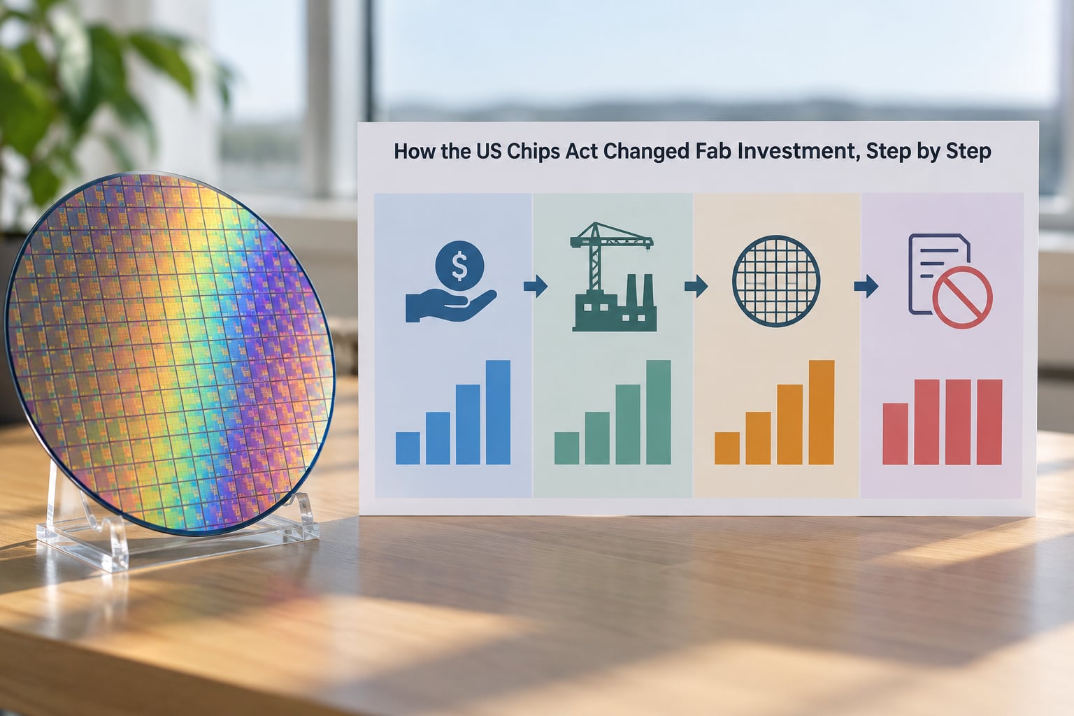
A company meets the Act in a fixed order, and the order explains most of the delays practitioners complain about. First comes a preliminary memorandum of terms with the CHIPS Program Office. Then a definitive award after a national-security review, a funding agreement, and disbursement tied to construction milestones. On top of that sits the tax credit, which is claimed later, after qualifying property is placed in service. Public research partnerships and the National Semiconductor Technology Center sit alongside rather than underneath the awards.
Appropriated grants and authorized tax spending move through different machinery, and the distinction is not academic. A grant is an appropriation: Congress budgets it, the Department of Commerce awards it, and money reaches the company in tranches as it builds. The Advanced Manufacturing Investment Credit is a reduction in what the company owes in tax, authorized separately at an estimated USD 24 billion, and it is only worth something to a company that has taxable income and qualifying property to place in service. A young or loss-making manufacturer can be awarded a grant and still wait years for the credit to matter.
Selection is competitive and scored, and the scoring is why the money concentrated. Projects that could demonstrate national-security value, a credible customer base, a real supply of skilled labor and willingness to accept guardrails scored better than speculative greenfield sites. Matching requirements add a private-capital test: the state or the company must carry part of the cost, which filters out projects that were never going to be built.
Conditions come attached from the start. A recipient accepts limits on expanding advanced capacity in foreign countries of concern, and in the last couple of years those conditions were being renegotiated in a small number of high-profile cases, which is why earlier award terms and current terms are not always identical. Applicants should read the current award document rather than a press release from 2023.
Which programs are funding new fabs?
Most readers assume the Commerce Department does all of it. It does not, and the other channels matter when you are trying to understand why a project moved. The table below covers the main funding routes a fab investment can draw on.
| Program | Typical recipient or project | Support structure | Investment decision it can change |
|---|---|---|---|
| CHIPS manufacturing incentives | Leading-edge logic, memory, analog and specialty fabs | Direct grants disbursed against construction milestones, plus loans | Whether a US site clears the capital committee at all |
| Advanced Manufacturing Investment Credit | Any qualifying manufacturer, including those without a grant | 25 percent credit against qualified property placed in service | Effective capital cost of equipment lines and expansions |
| National Semiconductor Technology Center and NIST research programs | Research consortia, shared facilities, packaging and test demonstrators | Competitive research grants, largely unspent so far | Which technical bottlenecks get shared tooling and talent |
| Defense Department and Microelectronics Commons programs | Trusted foundry and secure supply-chain capacity | Grants, facilities, and procurement commitments | Fabs with defense demand that commercial forecasts miss |
| Energy Department programs | Grid, utility, and high-load manufacturing infrastructure | Loan guarantees and infrastructure funding | Sites where power, not money, is the binding constraint |
| State and local incentives | Every major project, usually alongside the federal award | Property and sales tax abatements, land, infrastructure, workforce grants | Site selection between otherwise comparable locations |
| Green CHIPS | Communities hosting fabs | Competitive awards for childcare, utilities, housing and placemaking | Whether a community can actually support the workforce |
Two features of this landscape deserve attention. The research pot is the smallest and slowest-moving: only a small fraction of the roughly USD 11 billion National Science and Technology Initiatives fund had been allocated as of mid-2026, so in practice the Act has been a construction subsidy with a research label attached. And the state layer is where the local economics get decided, which is why two states can win the same project and still produce very different outcomes for the towns involved.
How incentives changed company decisions
What had to change in a project’s economics under the US CHIPS Act
A fab is justified on cash flows measured over two decades, while the political appetite for a subsidy is measured in months. The Act narrows that gap in three specific ways. A grant lowers the upfront capital requirement, which matters most for a first-of-a-kind US fab where a large share of the cost is site preparation, cleanroom construction and utility interconnection that no future expansion would need. The 25 percent credit lowers the effective cost of the equipment package, which is the part of a fab that scales with volume. Together they improve the utilization assumption a company is willing to underwrite, including capacity reserved for customers whose own demand is not yet locked in.
That last point is the one people miss. The binding constraint on advanced capacity has not been cost per wafer so much as the willingness to build for a customer who has not committed. A large, credible, conditional award functions as a partial substitute for a long-term supply agreement, which is why the first round of awards went overwhelmingly to companies with anchor customers already lined up.
What signals did manufacturers send in response?
There is a ladder here, and it is worth reading announcements against it. A preliminary memorandum is an intent to negotiate. A definitive award is a negotiated agreement that still has to be signed and funded. Groundbreaking means site work has started. Equipment orders and hiring show money is being committed to a specific line. A production milestone, with qualified volume wafers moving, is the first signal that a fab is real in the sense customers care about.
Each rung removes a different risk. The industry experience to date is that the rungs are widely spaced: practitioners consistently describe three to five years from site decision to a first wafer, which puts meaningful volume output for most of the current buildout around 2027 and 2028, with slippage accumulating at exactly the points most likely to be rushed, namely labor availability, utility permits and disbursement timing. Announced cost also includes far more than the federal award, since state incentives, supplier investment and site work are counted in the headline number too.
Where did investment shift geographically?
The regional pattern is easy to describe and easy to misread. Money went where power, water, land, labor and an existing supplier base could be assembled, not where incentives were largest in isolation. Texas, Arizona and New York took the largest individual projects; the Carolinas, Ohio, Indiana, Oregon, New York and New England took a long tail of fabs, packaging plants and supplier expansions.
| Region | What pulled projects there | Constraint that shapes the outcome |
|---|---|---|
| Southwest | Land at megafab scale, existing water and power investment, state incentives, proximity to West Coast customers and air cargo | Power generation and transmission, water rights, housing and childcare for a workforce arriving at once |
| Southeast | Established specialty-node and automotive clusters, port access, low-cost greenfield land, a deep tool and materials supplier base | Competing for the same toolmakers and construction crews as everyone else |
| Midwest | Low-cost power, university engineering talent, and an automotive and industrial customer base for mature and specialty nodes | Smaller sites, and less appetite for the newest process nodes |
| Pacific Northwest | Design and engineering concentration, clean hydro power, a strong advanced packaging and equipment ecosystem | Land scarcity and cost, and long permitting timelines |
| Northeast | Legacy fab sites that can be modernized cheaply, existing workforce, and immediate proximity to system designers | Brownfield constraints: older buildings, fragmented parcels, and costly brownfield remediation |
| Mid-Atlantic | Research institutions, federal facilities, and a foothold for compound semiconductor and photonics work | Land cost and a smaller supplier base than the Southeast |
The named awards behind those totals are worth having in one place, because the gap between federal support and announced project cost is the single most misread number in this topic.
| Company | Site | Direct incentives or credit announced | Announced project investment |
|---|---|---|---|
| TSMC | Arizona, including a second site | Direct incentives plus a 25 percent credit; total federal support announced at about USD 66 billion across chips and broader awards | About USD 40 billion for the second site alone |
| Micron | Idaho and New York, with a packaging facility in New Mexico | Direct incentives plus credit | Up to about USD 100 billion across the three states |
| Intel | Ohio, Arizona, Oregon, and restructuring at existing sites | Up to about USD 8.5 billion in direct funding and up to about USD 11 billion in loans | Multi-site buildout whose final scope has been revised |
| Samsung | Texas | Direct incentives plus credit | Advanced logic fab with a long production ramp |
| Texas Instruments | Texas and Lehi, Utah | Mostly tax credits rather than direct grants | Analog and embedded processing capacity for industrial and automotive customers |
| GlobalFoundries and Qualcomm | New York and other sites | About USD 4.2 billion combined in direct incentives | Mature and specialty nodes plus capacity reserved for a long-term customer agreement |
Read those two columns together and a pattern appears: the largest single checks went to memory, to leading-edge logic for AI accelerators, and to capacity secured by an anchor customer. Mature-node and specialty work, which is where most automotive and industrial shortages live, was funded more thinly, and advanced packaging arrived late enough that domestic high-bandwidth memory output was still effectively zero as of mid-2026 despite a great deal of announced capacity.
How the law reshaped the kinds of fabs being built
It is tempting to read the Act as a race to the smallest process node. It was not quite. Several distinct investment categories moved, and they respond to different buyers.
Leading-edge logic below 10 nanometers took the largest share, driven by AI accelerators and defense demand. Memory, including high-bandwidth memory and the packaging that pairs with it, took the single largest company commitment, because memory economics reward scale and location matters little once the site is chosen. Analog, power and embedded processors, the automotive and industrial workhorses, expanded mainly through tax credits rather than grants, and Texas Instruments is the clearest example of a company that expanded with credits and no grant at all.
Compound semiconductor and photonics work stayed smaller in dollar terms but grew in variety, often at research or demonstration scale rather than as high-volume fabs. Advanced packaging, once treated as the poor relation of fabrication, became its own investment category, which is the most structurally interesting change: the binding constraint on shipping AI chips is increasingly the package, not the wafer. And the National Semiconductor Technology Center is intended to fund shared research and packaging facilities rather than competing production capacity.
Taken together, the effect is broader than any single node. It is a widening of the domestic manufacturing base at every point in the stack, which is what supply-chain resilience actually requires, as opposed to a single prestigious process generation.
What guardrails came with federal support?
Federal money brings conditions, and these are the ones that affect investment decisions rather than public relations. Recipients pass a national-security review from the Department of Commerce, with additional review where an owner or partner is a foreign entity of concern. They accept limits on expanding advanced semiconductor capacity in China and other foreign countries of concern, and they face obligations around the movement of sensitive technology and personnel. There are workforce and childcare commitments, tied to the child-care construction requirement and to state and local partnerships, and there are reporting and audit obligations that continue for years after the ribbon cutting.
Awards are also conditional on milestones, and a project that misses them can face disbursement delays, renegotiated terms, or recovery of funds already paid. Clawback provisions are the reason the guardrails matter commercially: they convert a policy condition into a balance-sheet risk that a board has to price. Several recipients renegotiated their terms in the last couple of years, which is a reminder that an award announced in 2023 is a starting position rather than a fixed entitlement. Specific requirements continue to change as the rules and individual awards evolve, so anyone making a decision on the strength of an old announcement should check the current terms first.
What has the investment surge changed for suppliers?
The visible effect is on companies most readers never name. Construction contractors and engineering firms have had more semiconductor work than they can staff, and that backlog is the clearest near-term job creator in this story. Wafer fab equipment vendors and their tier-one suppliers, including the lithography, deposition and etch suppliers that dominate the tool market, are effectively sold out into the end of the decade, and orders from this buildout are a large part of why.
Materials suppliers, specialty gas and chemical companies, ultrapure water and waste treatment contractors, and electrical equipment makers are all clustering near the new sites, because a fab that cannot be supplied on a schedule is a fab that does not run at its design utilization. Advanced packaging providers, substrate makers and test houses are the newest members of this group and are among the least visible beneficiaries relative to their strategic importance. Utilities are participants too, financing generation and transmission upgrades to serve single customers with very large and very steady loads.
Two of these effects are temporary and one is durable. Construction hiring and startup staffing spike and fade; they are the first jobs and the least permanent ones. What persists is the supplier ecosystem that stays after a fab reaches steady state, and the tooling and materials relationships that make a second expansion cheaper than the first. Local labor markets feel both, and they feel them unevenly, because the same counties absorb a boom and a subsequent slowdown.
What are the economic benefits and the risks?
The case for the Act and the case against it are both made of facts, and the honest version puts them side by side.
| Objective | What has happened | What is still missing |
|---|---|---|
| Supply chain resilience | Announced leading-edge and memory capacity that did not exist in 2022, and a real US share of global capex | Volume output is mostly a 2027-2028 story, and advanced packaging and high-bandwidth memory were still not produced domestically as of mid-2026 |
| National security supply | Trusted foundry and defense-linked capacity receiving dedicated support | Concentration risk persists, and advanced nodes still depend on overseas materials and tools |
| High-paying jobs | Construction and supplier employment rising sharply in host counties | Federal funds per job run high relative to stimulus literature, and gains concentrate in construction and supplier services rather than in fab operations, which are capital-intensive with small headcount |
| Regional tax base and supplier demand | New property and payroll taxes, and long-lived demand for materials and equipment | A fab’s share of local tax revenue is smaller than its construction value suggests, and a single-plant county is exposed to one company’s roadmap |
| Technology spillovers | Research funding, packaging demonstrators and workforce programs at universities and national labs | Most of the roughly USD 11 billion research fund remained unallocated, so the spillover channel is the weakest part of the program |
The risks deserve equal space. Every subsidized fab carries a structural cost problem: industry estimates put US fab construction and operating costs roughly 30 percent above Taiwan’s, which does not vanish when a subsidy ends. Subsidy opportunity cost is real but unmeasured, and it competes with programs that might have produced more jobs per dollar. Overcapacity risk is the one that would most embarrass the program, because a fab market that loses its demand inflection in a couple of years turns a resilience investment into a stranded asset. And concentration in a handful of firms means a policy failure would be a corporate failure, which is what the guardrails were written to prevent.
Has the CHIPS Act guaranteed faster, cheaper, or more resilient chips?
No, and the gap between announcement and outcome is where most public confusion lives. A groundbreaking does not add capacity, because a fab that has not produced qualified volume wafers cannot ship a customer. A tax credit does not remove commercial risk, because it lowers cost and does not raise utilization. A fab in the United States does not guarantee cheaper chips, because the 30 percent cost premium is structural and export markets pay more for several reasons that have nothing to do with where a wafer was made. And no amount of domestic capacity solves dependencies that sit upstream, in tools, materials and packaging, or that sit in markets where the United States is a minority buyer.
What the Act can claim is a change in the direction and the durability of private investment, which the 28 percent capex share figure supports better than any ribbon-cutting photograph. If you want to track whether it is working, watch four things: whether projects reach a definitive award rather than a memorandum, whether construction starts on schedule, whether volume wafers qualify, and whether sites expand. Expansion is the strongest signal of all, because companies do not add square footage they expect to write off. A fifth indicator, harder to measure and more honest, is whether the tax credit gets claimed on schedule before its December 31, 2026 deadline for property placed in service.
One more question gets asked constantly and deserves a direct answer. The Act was not canceled. As of 2026 the awards, the guardrails and the investment credit remain in force, but the administration has pursued a revamp, including an investment accelerator framework, and the program has been reshaped in ways that changed terms for some recipients. Section 232 semiconductor tariffs and a second phase of tariff policy now sit alongside the credits, and several companies have described a freeze in decision-making while the interaction between tariffs and subsidies is clarified. The program is alive, contested and being rewritten at the same time, which is an unusual condition for industrial policy and explains both the momentum and the caution.
Frequently Asked Questions
Did the CHIPS Act pay for the full cost of new semiconductor fabs?
No. Direct incentives cover a minority share of a leading-edge fab’s project cost, and the 25 percent investment credit applies only to qualified property placed in service. Announced project totals include state and local incentives, supplier investment and the company’s own capital, which is why a project can carry a very large headline number and a much smaller federal one.
How are CHIPS Act grants different from investment tax credits?
Grants are appropriated money awarded by the CHIPS Program Office and disbursed in tranches as a company builds, subject to milestones and guardrails. The Advanced Manufacturing Investment Credit is separate authorized tax spending, claimed after qualifying equipment is placed in service, and it needs taxable income to be worth anything. A company can hold a grant and still wait years for the credit to matter.
Why do announced semiconductor fab projects cost more than the federal subsidy?
Because the headline number counts everything: the company’s own capital, state and local incentives, tax abatements, site preparation, utilities and the supplier investments that follow. A fab is a mixed project with a federal component, a state component and a private component, and only one of those three is what the Commerce Department actually awards.
Did the CHIPS Act end semiconductor supply shortages?
Not yet. Most of the current buildout will not produce meaningful volume wafers until roughly 2027-2028, and the segments that were tightest, including automotive mature nodes and high-bandwidth memory, remain substantially dependent on Asian production. Domestic capacity is growing from a low base, which is progress rather than resolution.
Which U.S. semiconductor companies received CHIPS Act funding?
The largest recipients include TSMC in Arizona, Micron in Idaho and New York, Intel across Ohio, Arizona and Oregon, Samsung in Texas, and GlobalFoundries with Qualcomm. Texas Instruments expanded largely through tax credits rather than direct grants. Awards for some recipients were renegotiated in recent years, so current terms may differ from original announcements.
Can a company lose CHIPS Act funding after receiving it?
Yes. Disbursement is tied to construction milestones, and a project that misses them can face delays, renegotiated terms or recovery of funds already paid. Recipients also carry ongoing compliance obligations around national security, expansion limits in countries of concern, and workforce and childcare commitments, and failing those can trigger the same consequences.
Conclusion
The US Chips Act changed fab investment by making domestic capacity something a board could approve on a five-year view instead of a twenty-year one, and the clearest evidence is that US share of global semiconductor capital spending is projected at 28 percent through 2032 against a 9 percent counterfactual. Everything else about the program is a work in progress, and the gap between announced dollars and qualified wafers is where the next several years of judgment will be made.
When you evaluate a specific project, check five things in order: whether it has a definitive award rather than a memorandum, whether construction has started, whether it is producing qualified volume output, whether it is expanding, and whether it still works commercially at a 30 percent cost premium. A company that clears all five has made an investment that will still be there in 2032. A company that stops at the first has announced a building.