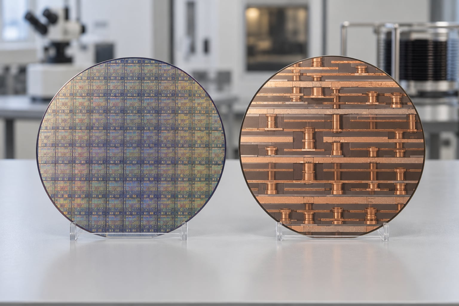
In semiconductor manufacturing, back end of line vs front end of line describes the two halves of wafer fabrication. Front end of line (FEOL) builds the transistors and other active devices in the silicon. Back end of line (BEOL) builds the metal interconnect layers that wire those transistors into a circuit that actually does something.
Once BEOL finishes, the wafer still has to be probed, diced, packaged and tested, and that last phase is a different thing entirely — usually called back-end manufacturing. Keep that distinction in mind, because mixing up BEOL wafer processing with back-end assembly and test is the single most common terminology mistake on this topic.
Table of Contents
- back end of line vs front end of line at a Glance
- What Is Front End of Line Semiconductor Manufacturing?
- What Is Back End of Line Semiconductor Manufacturing?
- How the Two Semiconductor Process Stages Differ
- Purpose and what each phase builds
- Process environment and thermal budget
- Equipment and materials
- Failure modes and yield
- A worked example
- Which Stage Comes First in Chip Production?
- Which Stage Matters More for Chip Design?
- Split manufacturing and IP trust
- Which Stage Is More Expensive or Time-Consuming?
- Frequently Asked Questions
- Is back end of line the same as semiconductor packaging?
- What is the main difference between FEOL and BEOL?
- Does the front end of line create the transistors?
- What happens during the back end of line?
- Can designers influence FEOL and BEOL decisions?
- Are FEOL and BEOL part of wafer fabrication?
- Which stage usually has more process steps?
back end of line vs front end of line at a Glance
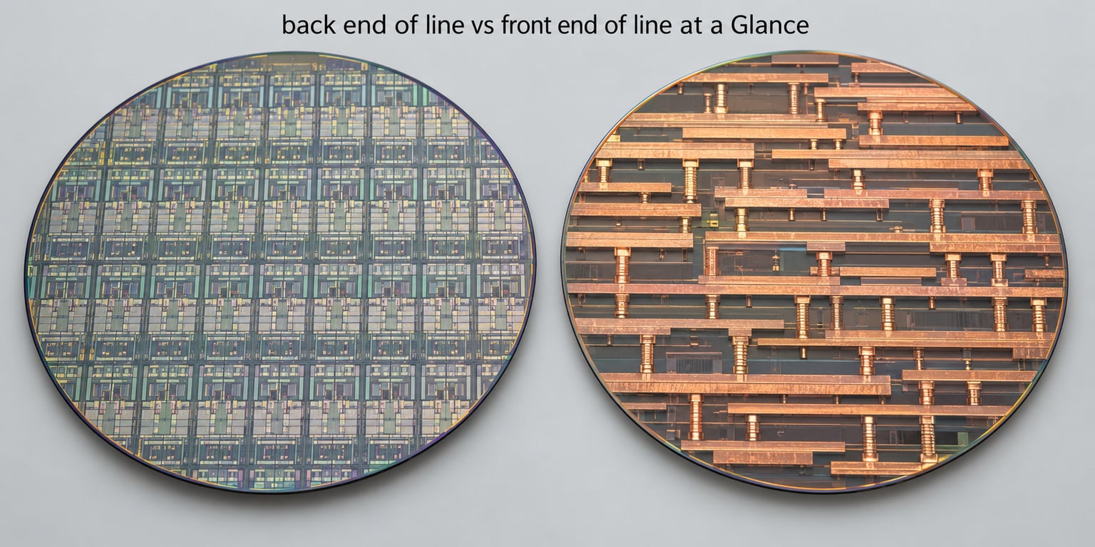
| Criterion | Front end of line (FEOL) | Back end of line (BEOL) |
|---|---|---|
| Purpose | Create the active device: transistor, isolation, gate stack | Connect the devices with metal wires and insulators |
| Output structure | Gate, source, drain and surrounding isolation in silicon | Multi-level metal stack plus passivation |
| Position in the flow | After wafer preparation, before MEOL | After MEOL, before wafer test and packaging |
| Key process steps | Oxidation, deposition, lithography, etch, ion implantation, anneal, CMP | Dielectric deposition, dual damascene etch, barrier and seed, copper plating, CMP, passivation |
| Dominant equipment | Lithography scanners, ion implanters, RIE etch, furnace and RTA, CVD/PVD/epitaxy | PVD/CVD/ALD, electroplating tools, CMP, wet cleans, overlay and film metrology |
| Dominant materials | Silicon dioxide, high-k dielectric, metal gate metals, photoresist, implant dopants | Low-k dielectric, copper, tantalum nitride barrier, seed metals |
| Typical defect classes | Particles, pattern defects, implant damage, oxide voids, shorted gates | CMP dishing and erosion, via opens, barrier breach, TDDB in low-k |
| Yield sensitivity | A killer defect anywhere in a die area usually kills the whole die | An open or short in one layer can kill a die, but redundancy and design rules absorb more |
| Node-scaling pressure | Lithography resolution, overlay, thermal budget, gate leakage | Line and via resistance, RC delay, metal pitch, EM reliability |
| Capex profile | Highest single-tool capital cost, concentrated in scanners | More tools overall, cheaper per tool, heavy on chamber count |
Public breakdowns of a modern logic process commonly divide the flow into roughly 35 sub-stations: around 11 in FEOL, 6 in MEOL, 9 in BEOL and 9 in assembly, test and packaging. Those counts vary by node and by company, but the shape is consistent — FEOL is fewer stations and far more expensive ones, BEOL is many repetitive stations at lower cost each.
What Is Front End of Line Semiconductor Manufacturing?
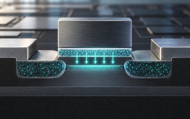
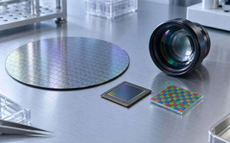
FEOL starts once the wafer is polished, cleaned and ready, and it ends when a working transistor with a gate, a source and a drain exists on every die. Everything before that point — wafer preparation from CZ-grown boule, slicing, lapping, polishing — is upstream of FEOL proper.
The sub-steps repeat many times, in a pattern that looks like this:
- Well and isolation formation. P-well, N-well and shallow trench isolation are etched into the silicon, with a thin liner and fill oxide to electrically separate neighbouring devices.
- Gate stack deposition. On older nodes a silicon dioxide gate oxide; on anything from 28nm down, a high-k dielectric plus a metal gate, because a thicker oxide with the same capacitance would leak too much.
- Gate patterning. Lithography transfers the gate shape from a reticle onto photoresist, and the resist pattern is transferred by anisotropic etch.
- Doping. Source and drain regions get boron, phosphorus or arsenic by ion implantation, with doses spanning roughly 1e13 to 1e16 ions per square centimetre depending on depth and concentration.
- Rapid thermal anneal. A spike anneal around 900-1100 degrees Celsius at roughly 100-200 degrees per second activates the dopants and repairs implant damage without melting the source and drain junctions.
- Silicide formation. A nickel or cobalt silicide is grown on the source, drain and gate to cut contact resistance.
- CMP. Chemical mechanical polishing flattens the surface to sub-nanometre flatness so the next lithography step has something level to print onto.
The output of FEOL is a wafer covered in isolated transistors with terminals waiting to be connected. Nothing on it computes anything yet.
What Is Back End of Line Semiconductor Manufacturing?
BEOL takes those terminals and builds the interconnect stack, usually ten or more metal layers on advanced logic, with copper in the lower and mid layers and thicker metals toward the top.
A modern interconnect build is one cycle repeated per layer:
- Dielectric deposition. An interlayer dielectric — a low-k material since the 90nm era — is laid over the previous metal and planarised.
- Contact and via etch. Vias down to the device terminals, then dual damascene patterning that cuts both the trench for a wire and the via for it in one lithography and etch sequence.
- Barrier and seed. A thin tantalum nitride or titanium nitride barrier is deposited, then a copper seed layer, to stop copper diffusing into the dielectric.
- Copper electroplating. The trenches and vias are filled from the seed by plating, which is far faster than sputtering at these depths.
- Polish. CMP removes the overburden copper and flattens the wafer again. Dishing and erosion are judged here.
- Repeat. Then passivation: a dielectric plus hard mask that seals the stack and protects it from moisture and handling damage.
Between FEOL and BEOL sits MEOL, the middle of line, which handles contacts and local interconnect — the M0 layer that reaches from the source and drain up to the first metal. It exists as a separate label because it carries its own thermal budget problems and its own contact resistance optimisation. There is no standard boundary: some companies book contacts as FEOL, some as MEOL, some as the first BEOL step.
How the Two Semiconductor Process Stages Differ
Purpose and what each phase builds
FEOL answers “what does this device do”. BEOL answers “how do the devices talk to each other”. A FinFET or gate-all-around nanosheet is entirely a FEOL object; the copper stack that carries its current is entirely a BEOL object.
Process environment and thermal budget
FEOL is a print-and-implant flow, dominated by lithography, ion implantation and high-temperature anneals, where each step has to fit inside a limited thermal budget so earlier junctions do not diffuse. BEOL is a deposit-and-fill flow at far lower temperatures, since copper metallisation and low-k dielectrics cannot tolerate the furnace temperatures FEOL uses.
Equipment and materials
Equipment vendors organise their application roadmaps around exactly this split — one etch supplier, for instance, publishes separate systems for FEOL, MOL and BEOL etch and surface prep. FEOL owns the lithography scanners, the implanters, the rapid thermal processors and the epitaxy tools. BEOL owns the deposition and plating tools, the CMP platforms, the wet cleans and the film and overlay metrology. The capital concentrates in FEOL; the tool count concentrates in BEOL.
Failure modes and yield
FEOL defects are mostly patterning and material defects: a stray particle bridging two features, an implant lobe outside the designed junction, a broken gate, an oxide void. Most are killer defects and there is no design workaround. BEOL defects are mostly fill and reliability defects: dishing and erosion from CMP, an unopened via, a barrier that breached, dielectric breakdown over time in a low-k material. When a fabless team sees a parametric yield problem at speed, the interconnect is usually the first place to look.
A worked example
Take one inverter gate. FEOL creates its FinFET, sets its threshold voltage through the work-function metals and dopes its source and drain. MEOL lands the contacts and the local interconnect. BEOL routes the gate input, the two data inputs and the output through copper, adds power rails thick enough to carry the current, and seals everything under passivation. Only then does wafer probe touch the die and confirm the inverter switches at the speed the design expects.
Which Stage Comes First in Chip Production?
FEOL always comes first, then MEOL, then BEOL. The full flow looks like this:
- Wafer preparation. CZ silicon sliced, lapped, polished, cleaned and inspected.
- FEOL. Active device formation: wells, isolation, gate stack, doping, anneal, silicide.
- MEOL. Contacts and local interconnect, the bridge from device terminal to first metal.
- BEOL. The metal interconnect stack, plus passivation.
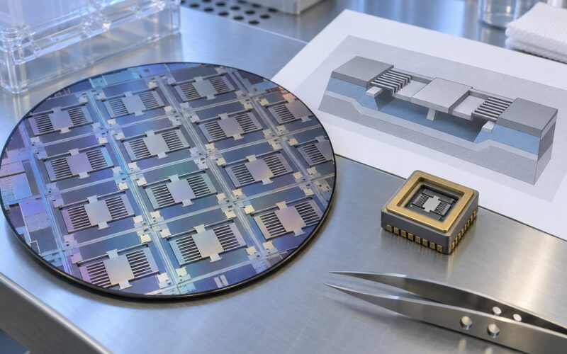
- Wafer test and packaging. Wafer probe, dicing, assembly at an OSAT, final test, and increasingly advanced packaging such as chiplets, 2.5D interposers and stacked HBM.
A full advanced logic chip runs 1,000-plus process steps and takes two to three months of fab cycle time end to end. Engineers who replicate a fab tend to describe it simply: FEOL is pretty much the same line everywhere, and BEOL is nearly the same line except where TSVs or other advanced structures appear.
Which Stage Matters More for Chip Design?
Both matter, and a fabless designer is exposed to both even though they own neither. FEOL decisions set transistor density, drive current, leakage and the device rules the PDK will let you draw against — you cannot route a wire narrower than the minimum metal pitch the process supports, and that pitch is a BEOL property. BEOL decisions then determine interconnect resistance, parasitic capacitance, signal integrity across a die, electromigration reliability and how much current your power grid can actually deliver.
BEOL is also where design effort is going now. At 3nm and 2nm, patterning is no longer the only wall — line resistance and RC delay in the upper metal layers are, which is why the industry moved toward ruthlessly thick top-level metals, backside power delivery and wider routing channels.
Split manufacturing and IP trust
One more design-side angle gets little airtime. In split manufacturing, FEOL is built at an untrusted foundry and BEOL at a trusted fab, so the probe houses that measure circuitry never see the sensitive transistor layer. It is a security strategy, not a cost one, and it is the clearest argument for treating FEOL and BEOL as genuinely separate stages rather than one long process.
Which Stage Is More Expensive or Time-Consuming?
There is no universal answer, and anyone who gives you a clean percentage for a specific node is guessing. What is true is where the drivers sit.
Cost: FEOL carries the highest single-tool capital in the fab. An EUV scanner is one of the most expensive pieces of equipment in any industry, and FEOL is where most of them sit. BEOL uses cheaper tools in much larger numbers, plus a great deal of consumables — copper plating chemistry, slurry, polishing pads, gases, wet clean chemicals. On memory and on older logic nodes, where there are many metal layers, BEOL consumables and chamber time can rival FEOL tool depreciation.
Cycle time: BEOL usually owns it. Each layer is a deposition, a lithography, an etch, a plating and a polish, repeated ten-plus times, and the steps must be serialised layer over layer. Advanced nodes use ruthlessly thick and tall metal stacks to cut resistance, and thick copper takes time to plate and time to planarise. FEOL, by contrast, is more parallel across the wafer and less additive in step count.
What actually decides it in a given fab: layer count, metal geometry, process node, tool set, and yield. Change any one of those and the split moves.
Frequently Asked Questions
Is back end of line the same as semiconductor packaging?
No. Back end of line (BEOL) is still wafer-level processing: it builds the metal interconnect layers on the wafer and ends with passivation. Packaging is the separate phase after wafer probe and dicing, where a die is mounted on a substrate, wire bonded or flip-chip attached, and tested, usually at an OSAT. The confusion comes from back-end manufacturing being a supply-chain term covering assembly, test and packaging while BEOL is a process term.
What is the main difference between FEOL and BEOL?
FEOL forms the active devices in the silicon, so it owns the transistor: the gate stack, source, drain and isolation. BEOL owns the wiring: contacts, local interconnect, the multi-level metal stack and passivation. In short, FEOL builds what each device does and BEOL connects those devices into a circuit. Everything a design team can do about speed, density and power comes out of one or the other.
Does the front end of line create the transistors?
Yes. That is exactly what FEOL is for. It starts from a bare wafer and, through oxidation, deposition, lithography, etching, ion implantation, rapid thermal anneal and CMP, leaves a wafer covered in working transistors with gate, source and drain terminals. The FinFET or gate-all-around structure itself is a FEOL object. What FEOL does not do is connect those transistors to each other, which is the job of MEOL and BEOL.
What happens during the back end of line?
BEOL deposits an interlayer dielectric, patterns contacts, vias and dual damascene trenches, lays down a barrier and copper seed, plates copper to fill them, and polishes the surface flat with CMP. That cycle repeats once per metal layer, often ten or more times on advanced logic, and finishes with a passivation layer over the whole stack. The result is a planarised wafer where every device is wired, powered and sealed.
Can designers influence FEOL and BEOL decisions?
Only within limits set by the process. A design team does not choose the gate stack or the metal stack, but it does choose device types, wire widths, routing channels, power grid topology and which metal layers carry which signals, all of which are judged against the foundry’s design rules and its characterisation data. PDKs, standard cells and memory compilers are how that influence is delivered. Outside those rules, you pick a process node, not a process.
Are FEOL and BEOL part of wafer fabrication?
Yes, both are stages inside wafer fabrication, the phase that turns a bare silicon wafer into a wafer full of completed dies. Wafer fabrication normally runs wafer preparation, FEOL, MEOL, BEOL, then wafer probe. Assembly and test come after, once the wafer has been diced. Public process breakdowns often count roughly 11 FEOL, 6 MEOL and 9 BEOL sub-stations, though the exact split differs by node and by company.
Which stage usually has more process steps?
BEOL usually has more, because the interconnect cycle repeats per layer. A single layer takes deposition, lithography, etch, barrier and seed, plating and polish, and advanced logic builds ten or more metal layers on top of each other. FEOL has fewer sub-stations but a much higher cost per step, since it owns the lithography scanners, implanters and thermal processing equipment. Fewer steps in FEOL, more steps in BEOL, higher cost per step in FEOL.
Back end of line vs front end of line comes down to one sentence: FEOL builds the transistors, BEOL wires them up, and packaging is a separate story that happens after both. If you are mapping a process, start by asking which phase a defect was born in. If you are handing a design to a foundry, read the design rules twice, because the front end sets what your circuit can be and the back end sets how fast and how reliably it runs. And when someone in a supply-chain meeting says back end, ask which back end they mean before you answer.