A copper interconnect is the on-chip wiring that carries signals and power between transistors, and an aluminum interconnect does the same job using a different metal. In the copper interconnect vs aluminum in chips question, copper wins on the layers that matter most: it carries about 40 percent less resistance, holds up far better under current stress, and let chipmakers raise clock speeds past the point where the wiring itself had become the bottleneck. Aluminum keeps a few jobs, mainly bond pads and the very first local metal layers, because those are cheap to make and easy to etch.
The catch is that copper is genuinely harder to build. It will not take a plasma etch, so the whole back end of the process had to be reinvented around a fill-and-planarize method called dual damascene. That rewrite, plus the barrier metal copper requires on every side, eats into copper’s raw advantage. If you only remember one thing, remember this: copper is the right default for advanced logic, and aluminum is the right answer for a short list of specific layers.
Table of Contents
- Copper Interconnect vs Aluminum in Chips at a Glance
- Electrical Resistance and Signal Speed
- How much does copper vs aluminum interconnect actually save?
- Why Aluminum Was Traditionally Used
- Why Copper Became the Performance Choice
- Electromigration and Reliability
- Manufacturing and Process Complexity
- Scaling, Geometry, and Design Rules
- Cost, Yield, and Practical Tradeoffs
- Which Should You Choose?
- Frequently Asked Questions
- Is copper always better than aluminum for chip interconnects?
- Why is aluminum still used in some semiconductor chips?
- Does copper interconnect increase capacitance in chips?
- Which interconnect material is better for advanced logic chips?
- Why does copper require a barrier and liner layer?
- Does copper interconnect always cost more to manufacture?
- Conclusion: Start With the Interconnect Requirement
Copper Interconnect vs Aluminum in Chips at a Glance
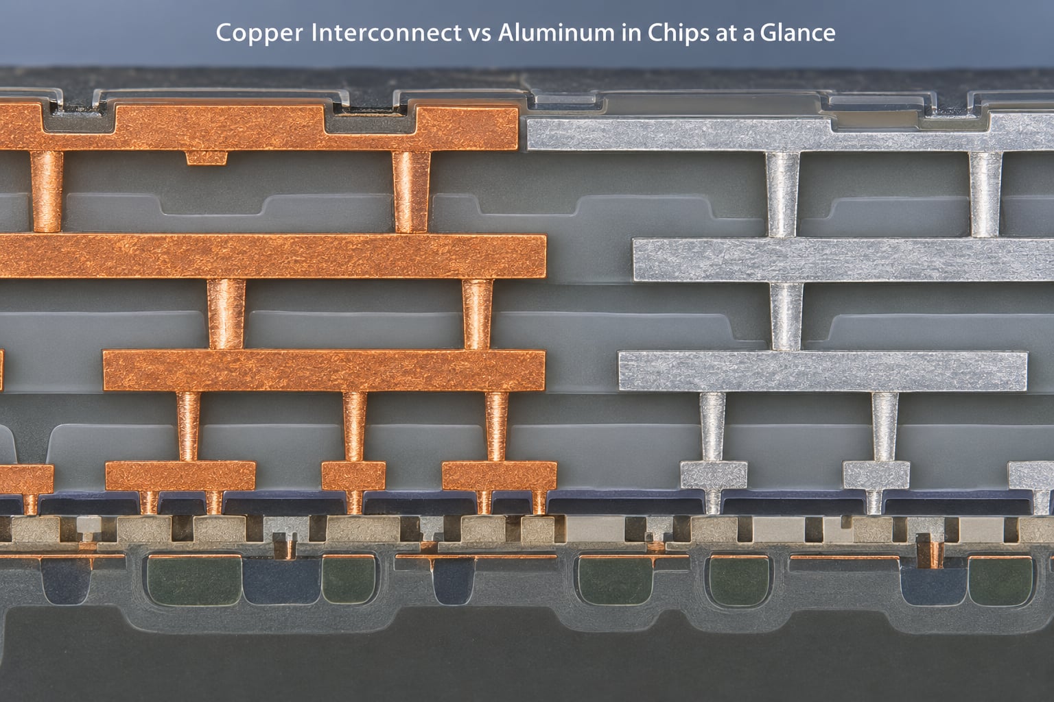
The short version of copper interconnect vs aluminum in chips is that copper buys speed and reliability and charges for it in process complexity. Here is the property-by-property comparison, with numbers at room temperature for bulk material where applicable.
| Property | Copper interconnect | Aluminum interconnect |
|---|---|---|
| Bulk resistivity | 1.68 micro-ohm cm | 2.65 micro-ohm cm (alloyed lines typically higher) |
| Line resistance at a fixed width | About 60 to 65 percent of an aluminum line of the same size | Baseline |
| RC delay in a given wire | Lower line R at the same capacitance, so lower delay | Higher line R, so higher delay |
| Patterning method | Additive fill: trench and via etch, liner, seed, electroplate, CMP | Subtractive: deposit a blanket film, etch it back to a line |
| Barrier and liner metal | Required, typically tantalum or tantalum nitride on trench and via walls | Not required for the conductor; a TiN or Ti/TiN layer is used for adhesion and contact |
| Electromigration margin | High, activation energy roughly 0.8 to 0.9 eV | Lower, roughly 0.5 to 0.6 eV, which is why silicon and copper are added to the alloy |
| Diffusion risk in silicon | Real; copper is a deep-level acceptor in silicon and needs the barrier | Low, aluminum does not create the same trap behavior in bulk |
| Etch and fill difficulty | No practical volatile etch by-products, so no plasma etch. Needs electroplating and CMP | Well understood plasma etch in fluorine and chlorine chemistries |
| Contamination exposure | Tool and chamber parts must be managed to avoid copper cross-contamination | Long-established handling, shared with CMOS tool sets |
| Where it is used now | Global signal and power wiring from 0.18 micrometer logic onward | Bond pads, the first local metal layers, thick power metal, some liner and seed roles |
One row deserves a caveat. Those resistivity figures are bulk metal numbers. A real damascene copper line is wrapped in a barrier and inset into a low-k dielectric, so the conducting cross-section is smaller than the drawn line width, and the measured line resistance lands somewhere around 60 to 70 percent of the aluminum line it replaced rather than the 63 percent bulk numbers suggest.
Electrical Resistance and Signal Speed
Copper has lower resistivity than aluminum, and that single fact is what drove the entire transition. Bulk copper measures 1.68 micro-ohm cm against roughly 2.65 micro-ohm cm for aluminum at room temperature. Wire resistance scales directly with resistivity, so a copper line of identical length and cross-section carries current with about 37 percent less resistance.
How much does copper vs aluminum interconnect actually save?
Two different numbers are worth keeping straight. The first is the material gain: about 37 percent lower resistivity for the same cross-section. The second is the gain in a real chip, which is smaller. Because copper needs a liner and a low-k dielectric around it, engineers can either widen the line or narrow the pitch. In practice the transition let teams narrow wires at the same current, which is what bought density.
Speed comes from RC delay. A signal on a wire is slowed by the resistance of the metal in series with the capacitance of the wire to its neighbors and to the substrate. Copper cuts the R term, and a copper wire with the same capacitance therefore settles faster. Across a whole die, interconnect delay stopped being a rounding error and became the dominant term, which is why the change happened at all.
Power follows directly. Dynamic power scales with capacitance times voltage squared, and static power in a given net scales with resistance times current squared. Lower resistance at the same capacitance means a design can hit a timing target at a lower supply voltage, and lower supply voltage is one of the cleanest ways to cut switching energy. Intel’s shift below 1.8 V around the same era was not a coincidence.
Current density is the other half. A copper line tolerates a higher current per unit cross-section before electromigration becomes a threat, so a designer can either carry more current through the same wire or shrink the wire. Shrinking is the direction the industry moved.
There is a persistent public belief that copper makes a chip run hotter, largely because copper is a superb heat conductor. It conducts heat about 1.7 times better than aluminum, and a good heat conductor in the metal stack is helpful rather than harmful. The real thermal story in a modern chip is that more of the metal is uncooled dielectric, and heat leaves through the back side of the die. Wiring material is not the dominant term in junction temperature.
Why Aluminum Was Traditionally Used
Aluminum was used on chips for decades because it was the only metal that fit the way fabs worked. It is deposited as a blanket film by physical vapor deposition, it lands straight on silicon dioxide with strong adhesion, and it etches cleanly in a plasma reactor using standard fluorine and chlorine chemistries.
That subtractive flow is simple and repeatable. Deposit everywhere, coat with photoresist, pattern the resist, etch the exposed metal everywhere else, strip the resist, done. Lines come out exactly where the resist said they would. The process was so well understood that aluminum stayed the default well past the point where its electrical limits were obvious.
Aluminum also carried a little silicon to prevent aluminum spikes from puncturing thin gate oxides during the patterning step, and later a small amount of copper to blunt the grain boundaries that drive electromigration. So the alloy was a slow accumulation of reliability patches on a material chosen first for ease, not for conductivity.
It was also simply available and understood at scale, with equipment, recipes, and trained process engineers already installed in every fab. Switching a mature production line to a new metal and a new patterning philosophy was not a small decision.
Why Copper Became the Performance Choice
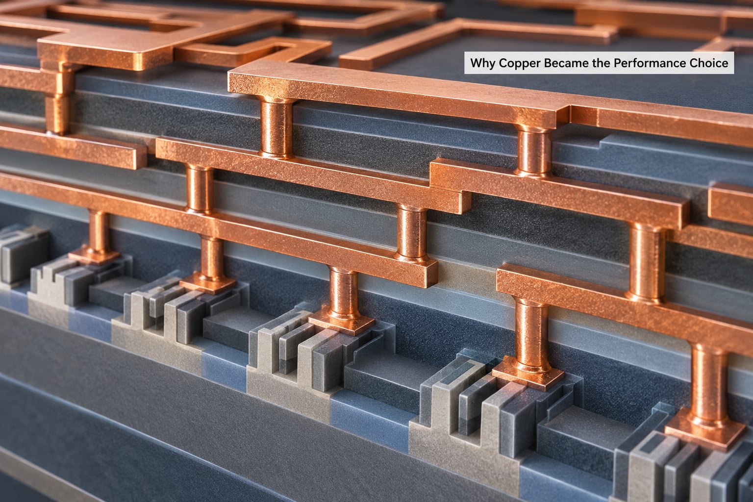
Copper won because interconnect resistance, not transistor switching speed, became the wall that stopped clock frequency from scaling. By the time processors were pushing toward 3 GHz, the delay in the wires between gates was longer than the delay inside the transistors. No amount of transistor improvement could compensate for slow wiring.
IBM and Motorola demonstrated working copper interconnects in 1997 at the 0.18 micrometer node, and the industry moved over the following several nodes. The recipe for the win was short and worth stating plainly. Copper wires have lower resistance for the same current, so dynamic power drops and delay falls. Higher current tolerance means a given line is far from its electromigration limit, which improves reliability. Lower resistance at the same capacitance lets the design run at a lower supply voltage, which cuts switching energy. And the same current fits in a narrower wire, which frees routing resources and lets a die hold more logic in the same area.
The transition was a process-control fight rather than a materials problem, and the engineers who shipped it said so repeatedly. Almost every early copper program stumbled on electroplating chemistry or on planarization consistency long before it stumbled on anything electrical. That is still the right summary of the tradeoff: aluminum is easier to manufacture, copper is better electrically, and the whole game is staying the process under tight control.
Electromigration and Reliability
Electromigration is the slow movement of metal atoms along a conductor driven by the flow of electrons. Atoms pile up at the end of a line and create voids that eventually sever it. This is the dominant wear-out mechanism in on-chip wiring, and it is why the reliability answer in copper interconnect vs aluminum in chips is not a footnote.
Aluminum electromigration is well characterized, and its activation energy sits around 0.5 to 0.6 eV. That is why early aluminum lines failed, and why the industry added small amounts of copper and silicon to the aluminum to break up grain boundaries and lengthen line life. The fix worked, but it patched an older material rather than solving the physics.
Copper is roughly half again to twice as fast in the Black’s equation sense, with an activation energy around 0.8 to 0.9 eV. Higher activation energy means far more thermal energy is needed to move an atom, so copper lines at the same current density last dramatically longer. This is the single most underrated advantage of the switch: reliability margin, not raw speed.
Copper introduced a different failure mode, though. Copper diffuses readily into silicon, and copper atoms in the silicon lattice act as deep-level acceptors. That traps charge carriers, which degrades the junction and can wreck leakage in a transistor. The barrier metal between the trench and the silicon is what stops this, and it is not optional.
Stress migration and corrosion follow the same logic. Aluminum is protected from the ambient by the interlayer dielectric around it, and aluminum itself is stable in that buried, oxidized environment. Copper does not oxidize reliably in the same way, so the seal and the barrier quality matter more. And when copper and aluminum meet in a moist environment, the pair forms a galvanic cell that corrodes the aluminum. Keep that in mind for the next section, where the two metals meet deliberately at the die and package boundary.
Manufacturing and Process Complexity
This is where the copper interconnect vs aluminum in chips comparison gets real, because the two processes look nothing alike. Aluminum is subtracted. Copper is built up.
- Aluminum flow, subtractive. Deposit a blanket aluminum film by PVD across the whole wafer. Spin a dielectric on top. Pattern the resist. Plasma-etch the exposed aluminum down to silicon dioxide. Strip the resist and fill the spaces with dielectric. Result: a line of metal sitting on a flat floor.
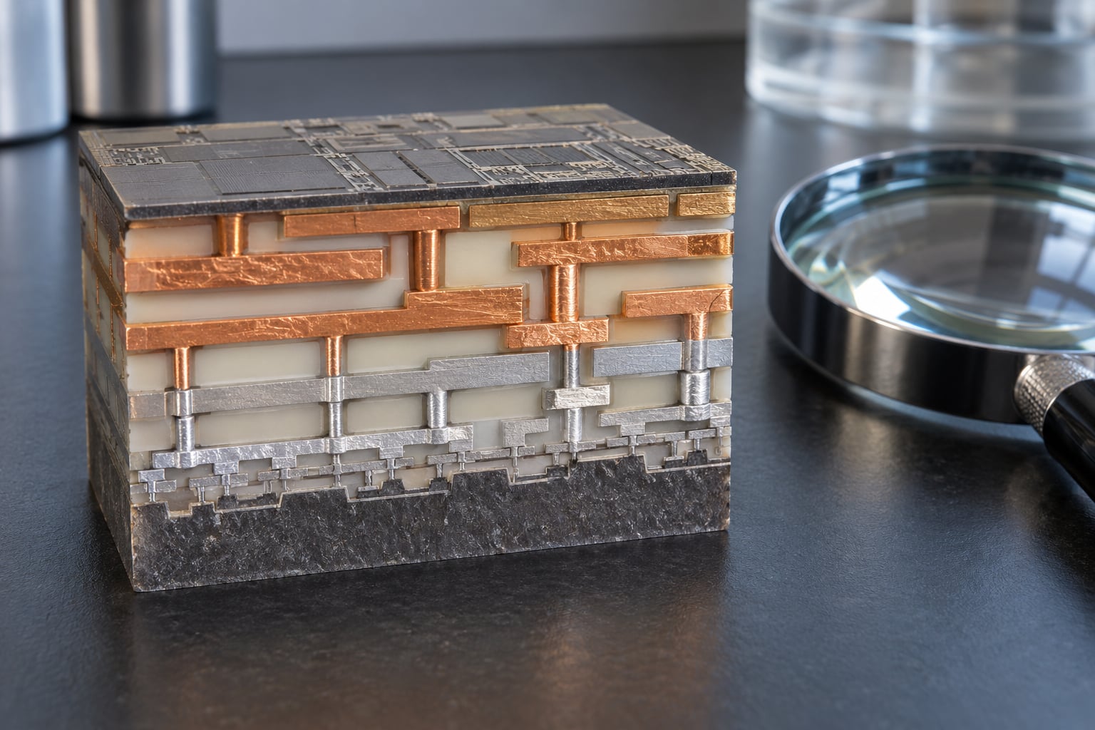
- Copper flow, additive. Pattern the low-k dielectric first, cutting trenches for wires and holes for vias. Deposit a dielectric liner, then a thin copper seed layer by PVD. Electroplate copper, which grows preferentially from the bottom up and fills the trench without leaving a seam. Polish everything flat with chemical-mechanical planarization, then repeat for the next layer with a dual-damascene sequence that does vias and wires together.
Dual damascene is simply the practice of forming the via and the wire in one combined sequence, so the via is embedded in the wire rather than made separately. It reduces the number of processing steps, which matters a lot when you are doing it a dozen times across a die.
The plating chemistry is one of the genuinely hard problems. Copper fills a narrow, high-aspect-ratio trench by superconformal deposition, meaning the growth front accelerates from the bottom and the sidewalls are suppressed. That requires a bath with an accelerator, a suppressor such as a polymer, and a leveller working at once, and the bath has to be controlled across every feature on a 300 mm wafer.
Then there is planarization. Electroplating leaves copper standing above the surrounding dielectric, and the next layer cannot be printed onto an uneven surface. CMP grinds the wafer flat while holding the copper lines in place, and copper CMP is a slow, expensive step that has to be repeated for every metal layer. Aluminum never needed anything like it.
Finally, copper does not stay in its lane. A stray copper atom on a tool part or a chamber wall can contaminate unrelated process steps, so fabs running copper maintain dedicated handling and cleaning practices. That overhead is invisible on a diagram and very real on a cost sheet.
Scaling, Geometry, and Design Rules
Design rules are the spacing and width limits a process can hold reliably, and they are where the geometry story shows up. As layers stack, a wire is a resistor sitting in a field, and its dimensions set both the delay and the crosstalk it picks up from its neighbours.
The first consequence of copper is that line resistance becomes the harder problem. Copper helps because the metal is better, but the barrier and liner occupy part of the drawn cross-section, so a designer cannot treat a copper line’s width as pure copper. In narrow lines, surface and grain-boundary scattering also push effective resistivity above the bulk figure, and the effective electrical mass problem gets worse as everything shrinks. Many teams now route the finest signals on lower-resistance local metals and use copper for the wide, long global wires where the total resistance actually matters.
The second consequence is fill. Copper plating fills a trench bottom-up, which suits tall narrow features, but the process still has an aspect-ratio limit, and a trench that will not fill properly creates a defect. Dielectric between lines has to be thin enough to keep coupling down and low-k enough to help, and the thinner the dielectric gets, the more mechanical damage it takes during CMP.
The third consequence is the via stack. A via in copper is a copper-filled hole through several layers, each one a chance for a defect, and the barrier, seed, and adhesion promoter all have to survive it. Contemporary nodes have also reduced the thickness of the low-k dielectrics, and integration of that change with copper fill has been a persistent engineering problem.
For design purposes, the pattern that emerges is consistent across markets. Advanced logic and high-performance processors put copper on the global signal and power layers. DRAM and NAND use copper for word lines and the upper metal stack, because current density and resistance both matter. Analog, RF, and mixed-signal designs use copper where resistance is critical and often keep aluminum on power and pad structures for process reasons.
Cost, Yield, and Practical Tradeoffs
Judging these metals by the price of the metal is the wrong test, because the wire is a small part of what it costs to build a layer. The real cost is the process around it. Aluminum needs a deposition tool, a coater and developer, and an etcher. Copper needs all of that plus a liner and seed tool, a plating bath, and a CMP tool for every layer, and it carries contamination control that aluminum never required.
Yield is the more interesting variable. A defect in a wide aluminum line is easy to screen out with a repairable memory cell. A plating void or a CMP scratch in a copper line is a killer defect that costs a whole die, and a defect rate that is small in each step compounds over a dozen layers. That is where the remembered industry stories come from: the early copper programs were hard, and the fabs that mastered electroplating chemistry and CMP consistency were the ones that shipped it at volume.
There is a quieter cost that never shows up in a process flow. Copper pulls the need for sputter tooling, seed deposition, and polishing into a back end that used to be simpler, and it makes any future switch to a different metal that much harder to imagine.
So the honest answer to the cost question is that copper is more expensive per layer and cheaper per unit of performance. For a 0.18 micrometer part where the interconnect is the bottleneck, that trade is obvious. For a mature analog part on a stable node where the wires were never the limiting factor, the extra tooling has to earn its keep somehow.
Which Should You Choose?
Choose copper for most advanced logic, most high-performance processors, memory word lines, and any design where interconnect delay sets the clock rate. Choose aluminum when process maturity, cost, or a specific layer function dominates. And expect mature nodes to use both.
The cases where aluminum still wins are specific. Bond pads remain aluminum because the wire bonder needs a soft, low-resistance surface that a gold probe will not scratch, and because the pad sits at the die edge where current density is low. The first local interconnect layers in many processes remain aluminum or an aluminum alloy, because those are narrow, short, and cheap to form. Thick power metal at the top of the stack is often aluminum for its mechanical and current-carrying reasons. And the seed and adhesion layers throughout the flow are often aluminum-family films, so the “copper process” still contains aluminum.
Then there is the movement past copper. At the smallest nodes, the local interconnect switched toward cobalt in some designs, because its shorter mean free path at very narrow widths resists the line resistance that fine copper cannot. Ruthenium has been studied as a liner and seed replacement, and tungsten remains a standard contact and local metal. The direction of travel is not a better copper, but a set of specialised metals chosen for specific layers.
Frequently Asked Questions
Is copper always better than aluminum for chip interconnects?
No. Copper is better on resistance, current capacity, and electromigration margin, which makes it the default from the 0.18 micrometer node onward for global signal and power wiring. Aluminum is still the better choice for bond pads, some local interconnect layers, and thick power metal, because those layers are cheap to make, easy to etch, and not the limiting factor. Mature nodes often use both metals in the same die.
Why is aluminum still used in some semiconductor chips?
Three reasons. Aluminum is deposited by sputtering and etched by well understood plasma chemistry, so it fits mature process flows and existing equipment. Bond pads need a soft surface that a probe will not scratch, which is exactly what aluminum provides. And several local and power layers were never limited by resistance, so the extra cost of a copper flow buys them nothing.
Does copper interconnect increase capacitance in chips?
Copper itself does not. It is a conductor and its dielectric constant is not the issue. The capacitance in a copper wire comes from the low-k dielectric placed around it and from the wire’s width and length. Switching from aluminum to copper mainly lowers the resistance term of the RC delay, and the capacitance term is handled by low-k materials and thinner dielectrics chosen separately.
Which interconnect material is better for advanced logic chips?
Copper, without much argument. Below 0.18 micrometers the wiring itself limits clock frequency, and copper’s lower resistance is what let processors push past that limit. Modern logic nodes use copper on global signal layers and copper or a low-resistance local metal on the finest layers, while aluminum survives on pads and selected power layers. The direction at the smallest nodes is toward metals such as cobalt for local interconnect.
Why does copper require a barrier and liner layer?
Copper diffuses readily into silicon, and copper atoms in the lattice act as deep-level acceptors that trap carriers and degrade transistor junctions. A thin refractory liner such as tantalum or tantalum nitride is deposited on the trench and via walls to block that diffusion. The liner also provides adhesion, because copper does not bond well to low-k dielectrics, and it carries current during electroplating in place of a thicker seed.
Does copper interconnect always cost more to manufacture?
Per process layer, yes. Copper adds liner and seed deposition, an electroplating tool, chemical-mechanical planarization at every layer, and contamination control that aluminum does not need. Per unit of performance, the picture is different. When wire resistance is the bottleneck on a given chip, copper lets the design hit its target at a lower supply voltage and a smaller die area, and that usually pays for the extra process cost.
Conclusion: Start With the Interconnect Requirement
Start by identifying what actually constrains the part. Is it clock rate, battery life, current per wire, die area, or cost? If interconnect resistance is the constraint, which it is for any high-performance logic design below 0.18 micrometers, copper is the answer, and the extra process steps are the price of the performance. That decision was made by IBM and Motorola in 1997 and refined by every foundry since.
Then check whether the constraint is really the metal. Bond pads, some local layers, and thick power metal are jobs aluminum still does better, and a mature analog or mixed-signal part on a stable node can be right to stay with it. If the part is at the smallest nodes, look past the two-metal framing entirely, because cobalt, ruthenium, and tungsten have taken over specific layers where copper’s own weaknesses show.
Either way, pick the interconnect material from the chip’s node, current, speed, and reliability requirements rather than from the metal’s bulk property sheet. The bulk numbers tell you which direction the trade goes, but the process, the geometry, and the layer’s actual job decide it.