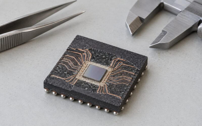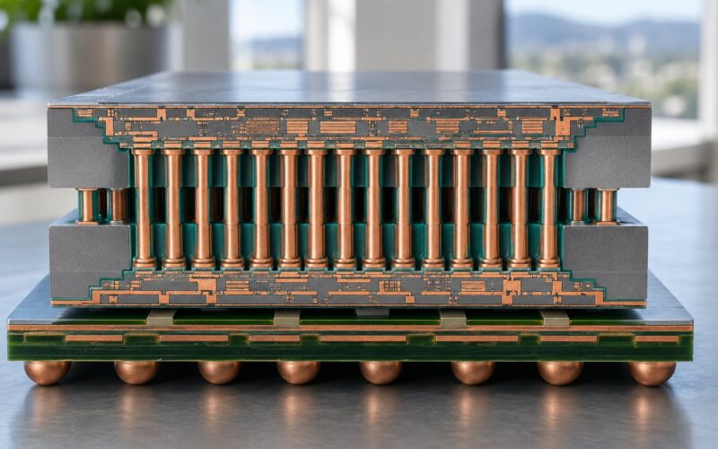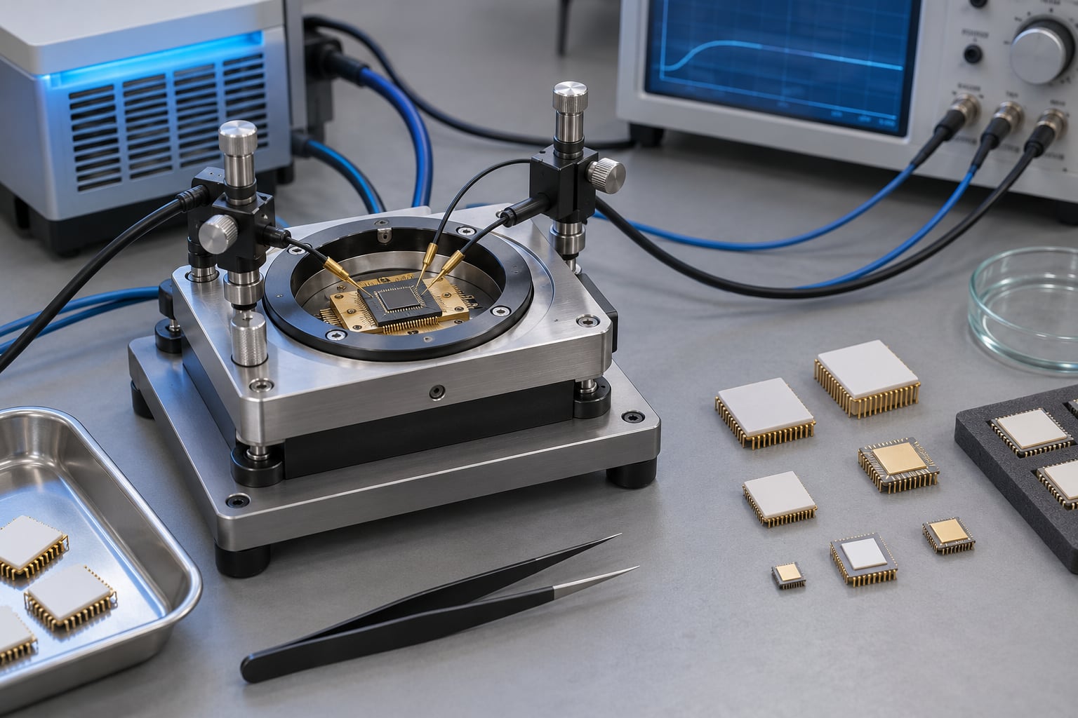
Reliability testing for semiconductors is the practice of putting a chip under controlled stress — high temperature, humidity, voltage, current, or temperature swings — until the failure mechanisms that would otherwise take a decade to appear in the field show up in a few hundred hours. Engineers measure what broke, why it broke, and how fast, then use physics models to translate chamber hours into years of expected product life.
It is not the same as testing whether the part works. A part can pass every electrical test at room temperature, ship at high yield, and still die in a car at 105 degrees. This guide covers what the stress tests are, what they look for, and how a test plan gets built.
Table of Contents
- What Is Reliability Testing for Semiconductors?
- Why Semiconductor Reliability Matters
- How Semiconductor Reliability Testing Works
- Reliability testing for semiconductors explained
- What Are the Main Semiconductor Failure Mechanisms?
- What Reliability Tests Are Used for Semiconductor Devices?
- How Do Burn-In and Accelerated Life Tests Differ?
- Which Reliability Metrics and Standards Matter?
- How Do You Choose the Right Reliability Test Plan?
- How Are Reliability Test Results Analyzed?
- What Are the Most Common Reliability Testing Mistakes?
- Frequently Asked Questions
- What is the difference between semiconductor reliability testing and burn-in?
- How long does semiconductor reliability testing usually take?
- How does accelerated life testing predict real-world semiconductor life?
- Does every semiconductor device need burn-in testing?
- What do JEDEC, AEC-Q100, and IEC reliability standards cover?
- Conclusion
What Is Reliability Testing for Semiconductors?
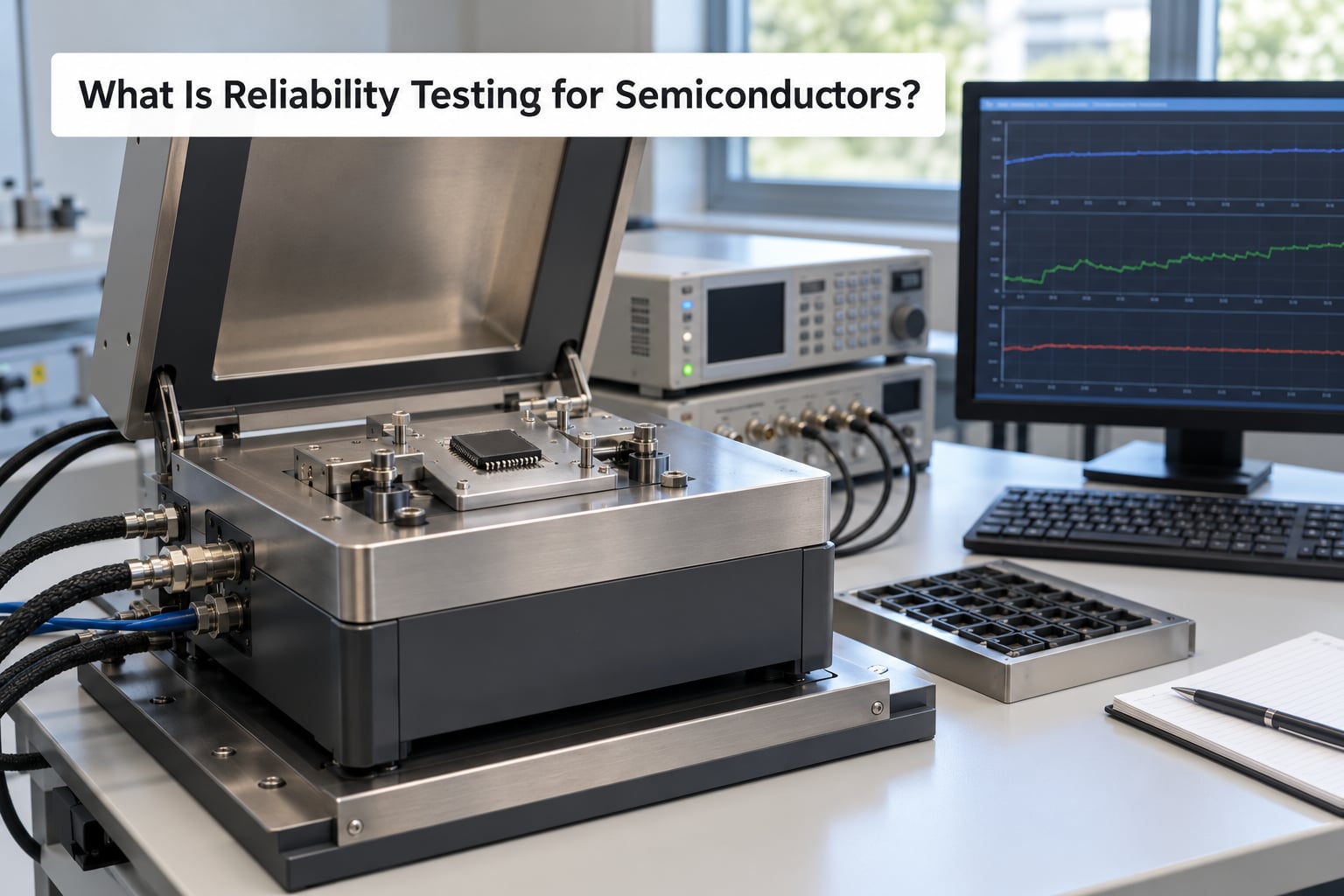
Reliability testing for semiconductors means deliberately stressing a device beyond its normal operating envelope to expose wear-out and latent defects, then measuring the results against a defined failure criterion. Reliability is a time-dependent property, so the test has to run long enough, at a high enough stress, to accelerate a mechanism that would otherwise take years to develop.
That separates it from three neighbouring activities. Functional testing asks whether the circuit does what it claims at nominal conditions, in seconds. Performance characterization maps speed, current draw, and timing across voltage and temperature corners to build datasheet numbers. Manufacturing screen (parametric test, burn-in) runs on every part leaving the line to catch obvious rejects. Reliability testing is slower, uses a small number of samples, and answers a statistical question: what is the failure rate over the product’s intended life?
Why Semiconductor Reliability Matters
A chip that fails in a phone is an annoyance. A chip that fails in an airbag controller, a pacemaker, or a traction inverter is a different category of problem, and the cost profile changes with it.
In automotive, medical, aerospace, and industrial equipment, a field failure means teardown, root cause, a corrective action report, and often a recall campaign. Warranty cost is only the visible part; the engineering time, the line stoppage, and the reputation hit add up quickly. Consumer electronics tolerate a low single-digit annual return rate because the product is cheap to replace. Data center silicon tolerates very little, because a failing accelerator can take an entire rack offline.
There is also the reputational math. Buyers in regulated markets ask for qualification data, and a supplier with weak field data loses design sockets that take years to win back. Reliability testing is cheaper than any of it.
How Semiconductor Reliability Testing Works
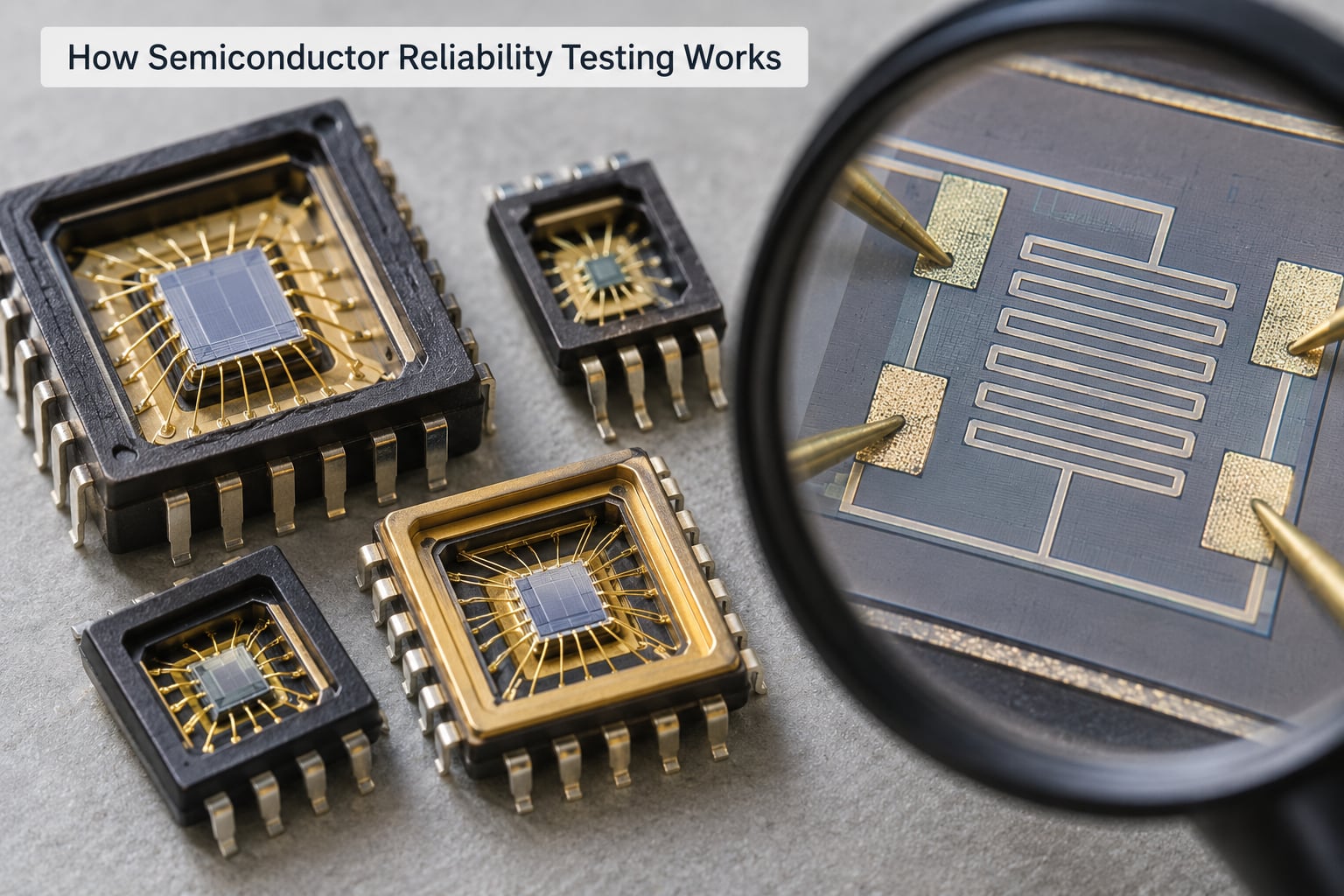
The workflow is consistent enough to describe as seven steps. You define the mission profile, select stresses, set failure criteria, pull representative samples, run the stress, analyse what failed, and compare the result to the required life.
- Define the mission profile. Junction temperature range, voltage, duty cycle, humidity, number of power cycles per day, and the required field lifetime — 10 years for automotive, three for a consumer peripheral.
- Select the stresses. Pick the accelerants (temperature, humidity, voltage, current density, thermal cycling) that map to the mechanisms the design is exposed to.
- Set failure criteria. Functional failure, drift past a parameter limit, increased leakage, or a rise in contact resistance. Write it down before the run starts.
- Choose samples. Parts from multiple lots and, where relevant, multiple assembly sites, so the result is not a single-lot artefact.
- Run the stress. Hold conditions and interrupt the test at intervals for intermediate measurements.
- Analyse. Fit the failure-time distribution, apply the acceleration model, and compute the acceleration factor.
- Decide. Extrapolate to field conditions and compare against the target, with a confidence interval and a safety margin.
Reliability testing for semiconductors explained
In plain terms, a stress test does something ordinary electrical tests cannot: it gives a defect time and energy to grow. A weak bond, a contaminated die surface, or a thin gate oxide is fine on the test bench and marginal in service. Raise the temperature and the voltage, and the defect rate moves from one per million per year to one per hundred per hour, which makes it measurable in a lab.
That is the whole trick. The test is not trying to break the part in a random way; it is trying to reproduce, in compressed time, the exact mechanism the part will meet in its application. Stress that triggers a different failure mode than the field one produces a confident number for the wrong problem.
What Are the Main Semiconductor Failure Mechanisms?
Every stress test maps to a mechanism, and the mechanism decides which test you run. The intrinsic ones live in the transistor and interconnect; the rest live in the package or come from the environment.
- Electromigration — high current density at elevated temperature moves metal atoms along the current path, thinning a line until it opens. Accelerant: current and heat.
- Stress migration — mechanical stress in a line at high temperature drives atoms with no current involved. Common in wide, cold lines.
- Hot carrier injection — energetic carriers cross the gate oxide and trap in it, shifting threshold voltage and reducing drive current. Worst in short-channel devices at high supply voltage.
- Bias temperature instability — the applied field alone splits bonds in the gate oxide, and the trapped charge degrades the device. Hits both polarities in a symmetric way.
- Time-dependent dielectric breakdown — a pinhole path grows through the thin gate dielectric until the device shorts. The dominant limit for advanced nodes.
- Moisture ingress and corrosion — water and ionic contamination reach conductors under bias, producing conductive dendrites or galvanic corrosion.
- Delamination — the mould compound or underfill separates from the die or die attach, opening a path for moisture and lifting thermal conduction.
- Bond and solder fatigue — repeated thermal expansion mismatch between die and substrate works the wire bonds or solder joints until they crack.
- Package cracks and seal failure — moisture gets in through a delamination path or a bad hermetic seal, and the internal atmosphere changes.
- Electrostatic discharge and electrical overstress — a transient event exceeds the device’s absolute maximum ratings and destroys the junction or gate structure outright.
- Latch-up — parasitic bipolar structures in bulk silicon conduct a large current triggered by a transient, holding on until the supply is interrupted.
What Reliability Tests Are Used for Semiconductor Devices?
This is the table most engineers print out. Each row is a stress, the standard that defines it, the accelerant, and the conditions a typical JEDEC qualification uses.
| Test | JEDEC reference | Accelerant | Typical conditions | Targets |
|---|---|---|---|---|
| HTOL — high temperature operating life | JESD22-A108 | Temperature, bias | 125 C, 1000 hours, at or above rated voltage | Electromigration, TDDB, BTI, HCI |
| HTRB — high temperature reverse bias | JESD22-A108 / A102 | Temperature, reverse bias | 85 to 150 C, 1000 hours | Surface leakage, junction integrity, oxide defects |
| Temperature cycling | JESD22-A104 | Thermal cycling | -40 C to +125 C, 500 to 1000 cycles | Die attach, solder joint and bond fatigue |
| Thermal shock | JESD22-A106 | Rapid temperature transfer | 10 s transfer, two chambers | Package cracking, delamination |
| THB / 85-85 | JESD22-A101 | Humidity, temperature, bias | 85 C / 85% RH, 1000 hours | Corrosion, moisture ingress |
| HAST / BHAST | JESD22-A110 | Humidity, temperature, bias | 110 to 130 C, 85% RH, 96 to 264 hours | Moisture-related corrosion in package and board |
| uHAST / autoclave | JESD22-A101 | Humidity, temperature, unbias | 121 C, 100% RH, 96 to 500 hours | Hermetic seal integrity, delamination |
| HTSL / high temperature storage | JESD22-A108 (bake) | Temperature | 150 C, 1000 hours, unbias | Die attach cure, passivation, wire bond |
| ESD — HBM and CDM | JESD22-A114 / A115 | Electrical overstress | ±2 kV HBM, ±500 V CDM typical | Gate oxide and junction ESD damage |
| Latch-up | JESD22-A105 | Current injection | ±100 mA on pins, 125 C | Parasitic thyristor paths |
| Burn-in / ELFR | JESD22-A108, JEP47 | Temperature, bias | Typically 24 to 168 hours near rated temperature | Infant mortality, weak die attach and bonds |
Power devices get their own set. A MOSFET or IGBT is qualified on high temperature reverse bias, avalanche ruggedness under repeated inductive load dumps, and short-circuit withstand time — the last being a matter of microseconds, so it is characterised rather than endurance-tested. Wide bandgap parts in silicon carbide and gallium nitride are tested harder still, because higher switching energy and junction temperatures punish weaker interfaces.
How Do Burn-In and Accelerated Life Tests Differ?
Burn-in screens out early failures; accelerated life testing characterises wear-out. They differ in purpose, duration, sample selection, and how results are used.
Burn-in runs near the rated operating temperature for tens to a few hundred hours on production parts, or a short high-temperature version on a sample. Its job is the left side of the bathtub curve — the infant mortality population caused by contamination, weak die attach, and defective bonds. Parts that survive burn-in are assumed to be past the steep drop.
Accelerated life testing runs to zero or few failures at conditions far above field use, over hundreds of thousands of device hours, to characterise the right side — the wear-out mechanisms. Results are fed into an acceleration model and extrapolated, not counted as a pass rate.
The mistake teams make is treating them as interchangeable. A part that passes 48 hours of burn-in has not demonstrated 15 years of electromigration margin, and a 1000-hour HTOL run on three lots is not a way to reject units individually.
Which Reliability Metrics and Standards Matter?
The core metrics are failure rate (or hazard rate), mean time to failure, acceleration factor, and confidence level — with FIT as the industry unit of measure.
One FIT is one failure per billion device hours. A 10 FIT part is expected to produce roughly one failure per 100 million hours of operation, which for a single device is a small annual probability but adds up across a large fleet. Field programs usually quote defect levels in DPPM (defective parts per million) as well, since that is what a customer sees on an incoming quality report.
The bathtub curve remains the useful mental model: a high early failure rate, a long low plateau where nothing much happens, then a rising wear-out rate. Sample size selection is driven by the plateau, because that is the region where a zero-failure run has to demonstrate something. With zero failures in n devices, the one-sided lower bound on reliability at time t at confidence c is R = 1 – c^(1/n), which is why 77 units with no failures supports roughly 95% confidence that reliability exceeds about 96% over the test interval — and why 231 units supports 99%.
Acceleration factors come from models, and the choice matters:
| Model | Primary application | Stress variable |
|---|---|---|
| Arrhenius | Temperature-driven degradation: TDDB, electromigration, corrosion | Absolute temperature, activation energy |
| Eyring | Arrhenius plus a second variable, typically humidity | Temperature and relative humidity |
| Black’s equation | Electromigration in aluminium lines | Current density, temperature |
| Coffin-Manson | Thermo-mechanical fatigue from temperature cycling | Temperature excursion rate and range |
| Inverse power law (E-model) | Time-dependent dielectric breakdown | Electric field |
Standards organise the whole thing. JEDEC writes JESD22 method documents (A108 for temperature life, A104 for temperature cycling, A110 for HAST, A101 for humidity) and JESD47 for the flow of a product qualification. AEC-Q100 sits on top for automotive parts and adds severity grades, specific sample counts, and requalification triggers. MIL-STD-883 governs defence and space, and IEC 60068, 60749, and 61709 cover the generic and industrial space, including the IEC 62380 reliability data handbook format for FIT reporting. None of them is universal — the customer contract and the end market decide which applies, and parts frequently need two or three at once.
How Do You Choose the Right Reliability Test Plan?
A test plan starts from the application, not from a standard’s default menu. Work through these inputs in order.
- Application risk and required lifetime. Automotive and medical parts target 15 years or 10,000 hours of operation; a consumer part may be three.
- Operating temperature range. The gap between worst-case ambient and junction temperature sets the temperature accelerant.
- Voltage and current density. A high-performance processor at its maximum supply voltage is far more exposed to TDDB and HCI than a low-voltage sensor.
- Humidity and environment. Sealed versus open package, conformal coating, and whether the board assembly is included change the humidity test choice completely.
- Package and materials. Organic substrates, mould compounds, underfill, and the number of thermal cycles in service decide whether cycling or moisture testing matters more.
- Prior failure history. A field return for delamination earns a bigger test sample, not a new test.
- Certification requirements. AEC-Q100 or a defence programme sets the mandatory matrix and sample counts on top of your own.
- Sample budget and calendar. Realistic programmes run 77 to 231 devices per condition, with 1000-hour HTOL and 96 to 264-hour HAST, so a full qualification lands somewhere between six and twelve months when tests run in parallel.
How Are Reliability Test Results Analyzed?
Analysis is where a test turns into an engineering decision, and the order of steps matters. First confirm the acceleration did not change the physics: failures caused by a different mechanism at the stress condition than the one seen in the field invalidate the extrapolation. That check is the single most valuable thing a reliability engineer does.
Then look at the distribution, not just the count. A Weibull plot of failure times separates early-life failures from a wear-out population, and a straight line on that plot tells you the shape parameter and the characteristic life. If the data show a cluster of early failures mixed into a wear-out run, the average is meaningless and the two populations have to be analysed separately.
After that, apply the model, compute the acceleration factor, and report the result with a confidence interval. Zero-failure runs need a one-sided lower bound, not a claim of “zero risk”. Finally, compare failure codes across conditions: the same failure mode under temperature, voltage, and humidity stress is strong evidence of a real mechanism, while a scattering of unrelated codes is a sign of test-induced damage or an unsuitable stress.
What Are the Most Common Reliability Testing Mistakes?
Most qualification programs that go wrong share a small number of causes.
- Unrealistic stress conditions. Pushing past the point where the dominant mechanism changes produces a result that describes a device nobody will build.
- Too few samples. 30 units with zero failures says almost nothing; the sample size is what buys confidence.
- Testing only ideal parts. Building samples from the best wafer and best assembly lot hides the tail that actually shows up in volume.
- Using the wrong acceleration model. Arrhenius is not a universal constant. A wrong activation energy can move a lifetime estimate by an order of magnitude.
- Overlooking package interactions. Testing a die-level part and assuming the packaged part is equivalent misses mould compound stress and moisture path changes.
- Ignoring lot variation. Three units from one lot is one data point, not a population. Document lot-to-lot spread explicitly.
- Treating a completed test as proof of lifetime. A pass is evidence within a confidence interval at a stated model. It is not a guarantee.
- Over-burning parts. Excessive burn-in stress can itself damage the product, and a rejected unit that would have shipped fine is a self-inflicted yield loss.
Frequently Asked Questions
What is the difference between semiconductor reliability testing and burn-in?
Reliability testing answers a statistical question about lifetime: it stresses samples hard for hundreds or thousands of hours, then extrapolates the result to years of field use. Burn-in screens individual production parts at a milder stress to remove infant mortality, the early failure population. In short, qualification tells you how long the design lasts; burn-in tells you which units are sound enough to ship.
How long does semiconductor reliability testing usually take?
A single test is rarely longer than a few weeks. A 1000-hour HTOL run takes about six weeks on a real chamber, HAST typically runs 96 to 264 hours, and temperature cycling of 1000 cycles takes one to two months. A full qualification matrix on near-production silicon usually takes six to twelve months, because many of these tests run in parallel rather than one after another.
How does accelerated life testing predict real-world semiconductor life?
You run the stress well above field conditions, measure how many failures occur in that time, and divide by an acceleration factor calculated from a physics model such as Arrhenius, Black’s equation, or Coffin-Manson. That factor converts chamber hours into equivalent field hours. The prediction is only credible when the stressed failures show the same physical mechanism as the field failures you expect to see.
Does every semiconductor device need burn-in testing?
No. Burn-in pays for itself mainly where early-life failure rates are high and the cost of a field failure is high: high-voltage analog parts, power devices, large dies with long leads, and automotive or medical grade products. Low-power digital parts, memory, and well-controlled mature processes usually show a much smaller infant mortality population, so sampling screens or wafer-level reliability monitors cover the risk instead.
What do JEDEC, AEC-Q100, and IEC reliability standards cover?
JEDEC sets the method documents and the qualification flow: JESD22 covers individual test methods such as temperature cycling and HAST, while JESD47 defines how a product qualification is assembled and what it must include. AEC-Q100 applies that JEDEC base to automotive parts, adding severity grades, mandatory sample counts, and requalification triggers. IEC standards, including IEC 60068, 60749, and 62380, cover generic and industrial environments plus reliability data reporting.
Conclusion
Reliability testing for semiconductors works best when you start with two things before you pick a single chamber: write down the environment your part will actually see, and define what counts as a failure. Everything after that — which stresses, which standards, how many samples, which acceleration model — follows from those two statements.
Choose tests that reproduce the relevant failure mechanism without inventing a failure mode the product will never experience, and treat every extrapolated lifetime as a number with a confidence interval attached. That is the difference between reliability data a customer can act on and a qualification folder nobody trusts.