How multilayer PCBs are built comes down to one idea: each copper layer is patterned on its own core, inspected, then everything is pressed into a single board and tied together with plated vias. A multilayer PCB is a printed circuit board made from three or more copper layers separated by insulating dielectric and permanently bonded together under heat and pressure. A fabricator typically runs 13 stages between the design data and the tested board.
Table of Contents
- How Multilayer PCBs Are Built: From Design to Final Test
- Step, equipment, and the defect that step usually causes
- How a four-layer board is actually built
- What Is a Multilayer PCB?
- How Many Copper and Insulating Layers Are Used?
- Why more layers is not always better
- Where multilayer boards end up
- What Design Data Does the PCB Manufacturer Need?</
- How copper weight changes what a design can do
- Which base material the stack should use
- How Is the Copper Pattern Transferred Onto Each Layer?
- How Are the Layers Aligned and Bonded Together?
- How Are Vias and Other Holes Formed?
- Which via type to use
- How Is Copper Added Inside the Holes?
- How Are Outer Layers Patterned After Plating?
- What Finishes and Surface Treatments Are Applied?
- How the panel is cut into boards
- How Is a Completed Multilayer PCB Inspected and Tested?
- Frequently Asked Questions
- Are multilayer PCBs stronger than double-sided PCBs?
- What is the minimum number of layers for a multilayer PCB?
- How are the layers inside a PCB connected?
- What is the difference between a four-layer PCB and a four-layer build-up PCB?
- How thick can a multilayer PCB be?
How Multilayer PCBs Are Built: From Design to Final Test
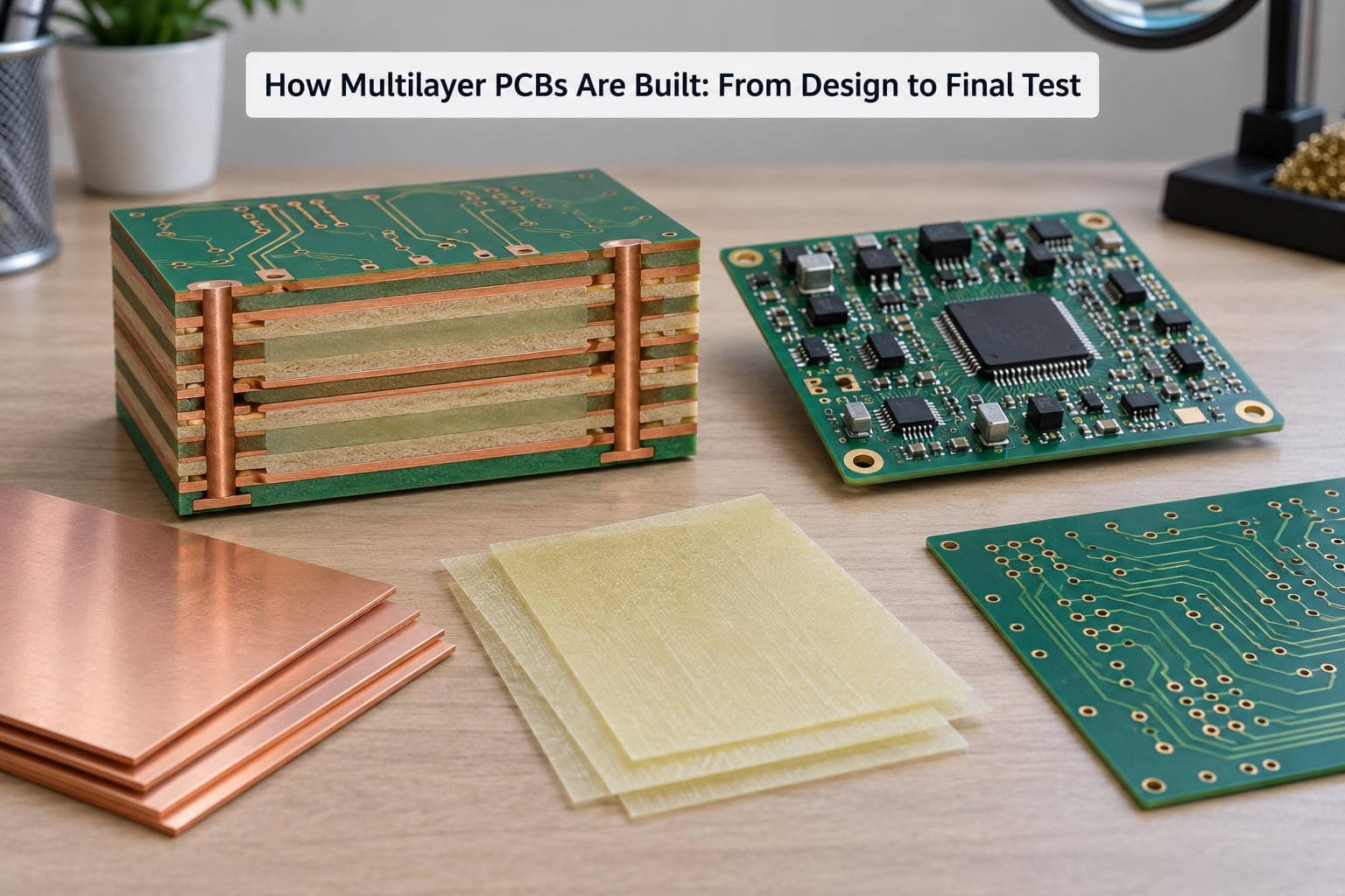
Two things make a multilayer board different from a double-sided one. The inner layers carry signal, ground, or power artwork and are sealed inside the stack, so the factory has to drill and plate through the finished thickness to reach them.
The ordered flow below is how multilayer PCBs are built in a conventional fab. The exact sequence shifts with layer count, material choice, blind or buried via requirements, surface finish, and whether the build is a standard rigid stack or an HDI build-up.
- Data review and stackup confirmation. The manufacturer checks Gerber or ODB++ data, drill files, fab notes, impedance targets, and the layer stack before anything touches copper.
- Material preparation and preconditioning. Copper-clad cores and prepreg are cut to panel size, cleaned, and typically held in a controlled environment for 24 to 48 hours so moisture content is even.
- Inner layer imaging. Each inner core gets a cleaned surface, a laminated photoresist film, exposure through artwork, and development so only the intended traces stay protected.
- Inner layer etching. Unprotected copper is stripped chemically, leaving the signal, ground, and power artwork behind on the core.
- Inner layer inspection. Automatic optical inspection and, where required, electrical probing confirm the artwork matches the source data and that the layer is free of opens and shorts.
- Surface preparation for bonding. Inner cores are treated with an oxide or coupling treatment so the prepreg resin bonds to the copper surface rather than to a contaminated one.
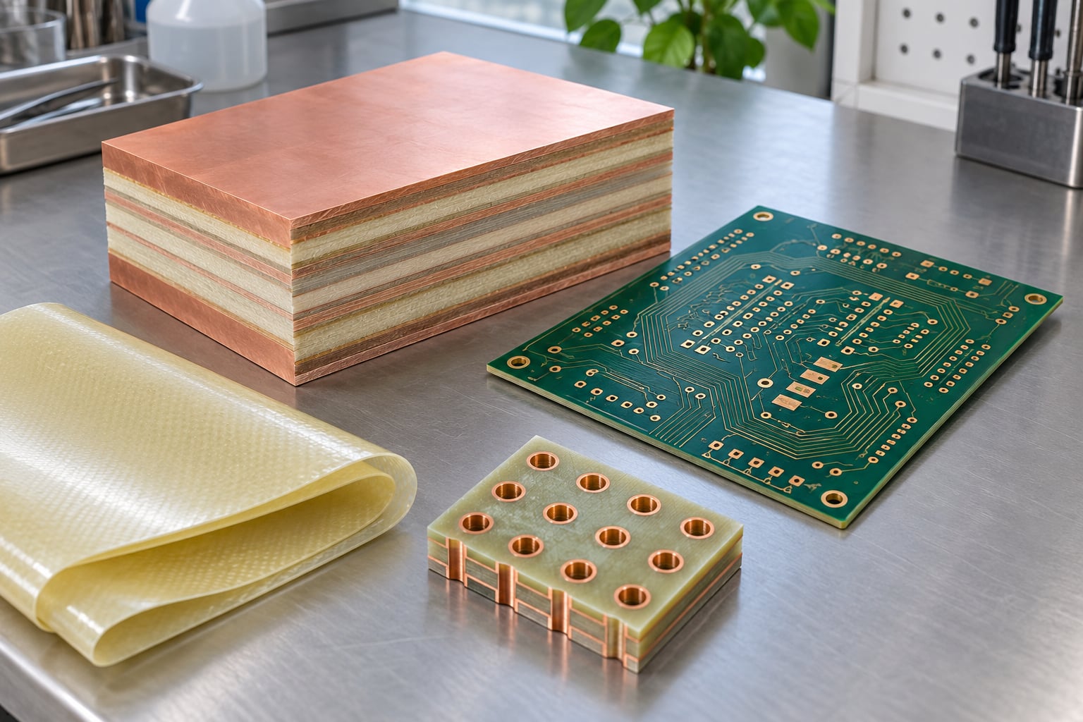
- Stacking and lamination. Prepreg, core, and copper foil are aligned to the stackup and pressed through a controlled heat, pressure, and time cycle that consolidates the panel into one solid board.
- Drilling. Mechanical drills make through-holes and larger blind or buried holes; a CO2 or UV laser makes microvias and small blind vias in a build-up process.
- Desmear, activation, and seeding. Hole walls are cleaned of resin and drilled debris, micro-etched to fresh copper, and coated with a thin electroless copper layer.
- Electroplating. The seeded panel is plated in a copper sulfate bath so the hole barrels, pads, and surface traces build to the target copper weight.
- Outer layer patterning. The plated surface is imaged with dry film or direct imaging, developed, and etched to leave the finished outer copper artwork.
- Solder mask, legend, and surface finish. Liquid solder mask is screened, cured, and developed; legend is printed; the exposed copper receives HASL, ENIG, immersion silver, tin, OSP, or hard gold.
- Profiling, inspection, and electrical test. The panel is routed, V-cut, or punched into boards, then dimensionally checked, AOI inspected, X-ray inspected, and electrically tested against the netlist.
Step, equipment, and the defect that step usually causes
Most quality escapes on a multilayer board come from a handful of steps. This table pairs each stage with the equipment and chemistry involved and the failure a fabricator actually looks for afterwards.
| Stage | What happens | Equipment or chemistry | Defect seen here |
|---|---|---|---|
| Preconditioning | Moisture in cores and prepreg is equalised over 24 to 48 hours | Controlled-environment holding cabinet | Blistering and delamination at the press if skipped |
| Inner imaging | Resist is applied, exposed, and developed to define the artwork | Dry film laminator, laser direct imaging, developing tank | Registration error, resist residue, incomplete exposure |
| Inner etching | Exposed copper is stripped, leaving the retained artwork | Ferric chloride or cupric chloride etchant | Etch loss on fine traces, copper nicks, bridging |
| Inner inspection | Artwork is compared to the source data and probed | AOI, optional electrical test | Missing trace, shorts, damaged pad caught before lamination |
| Lamination | Stack is pressed so prepreg resin flows and cures | Multi-day press cycle, heat and pressure, vacuum lamination for void control | Delamination, resin flow shifting dielectric thickness, warpage |
| Drilling | Through-holes and via holes are formed through the full thickness | NC drill, CO2 or UV laser drill | Breakout, barrel-to-barrel misalignment, bit wear, heat damage to resin |
| Desmear and seed | Hole walls are cleaned and coated with a thin copper layer | Permanganate or plasma desmear, micro-etch, electroless copper | Resin-filled hole, starved seed layer, poor adhesion |
| Plating | Copper builds to target weight on barrels and surface | Acid or alkaline copper bath, pulse plating for high aspect ratios | Void in a barrel, under-plated hole, copper nodules |
| Outer imaging and etch | Plated surface is imaged and selectively stripped to artwork | Dry film or liquid resist, LDI, etchant | Over-etch, shorts between adjacent outer traces |
| Mask and legend | Solder mask and reference designators are printed and cured | Screen print or LPI, UV or thermal cure | Mask contamination of pads, misaligned legend, poor adhesion |
| Surface finish | Exposed copper is coated for solderability and wear resistance | HASL, ENIG, immersion silver, tin, OSP | Thin or contaminated finish, black pad on immersion gold |
| Profiling and test | Panel becomes individual boards and is verified | V-score, router, flying probe, fixture test, X-ray, microsection | Opens, shorts, annular ring below spec, out-of-tolerance impedance |
How a four-layer board is actually built
A four-layer board is the most common multilayer build, and its flow is the shortest path to understanding the rest. Two inner cores are cut, cleaned, imaged, etched, and inspected separately. Each is then treated for bonding, and the stack is assembled as outer copper foil, prepreg, inner core 1, core material, inner core 2, prepreg, outer copper foil.
That stack goes through one press cycle. It is drilled through for plated through-holes and surface pads, prepared, seeded, and copper plated, which is the first point where all four layers become electrically common. The outer layer is imaged and etched, then mask, legend, and finish follow, and the panel is profiled and tested.
Compare that with a two-layer board. A double-sided board skips every inner imaging, etching, inspection, and bonding stage: copper is applied to both sides of one core, drilled through, plated once, then the outside is etched. Fewer steps, one press cycle or none, and no interlayer alignment to hold. That gap is exactly why two-layer is the right answer for a low-density design and the wrong one the moment return paths and crosstalk start to matter.
What Is a Multilayer PCB?
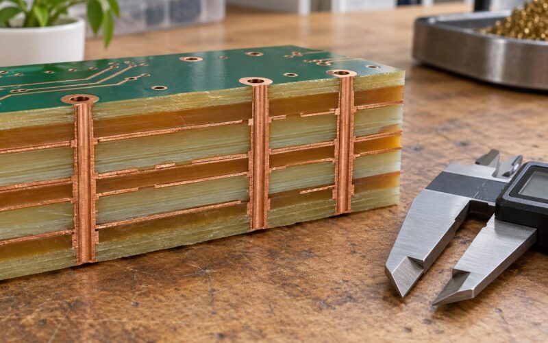
A multilayer PCB is any board where two or more copper layers are tied together through an insulating core. The conductive layers are separated by prepreg or a core sheet, and vertical vias carry signals, power, and ground between them. In everyday fab usage the term means three or more copper layers.
The reason engineers reach past two layers is space and signal behaviour. A four-layer board puts a solid ground plane directly under a signal layer, so the return current has a continuous path and radiated noise drops sharply. It also cuts the board area needed for a given net count roughly in half.
| Board type | Copper layers | Typical connection | Common use | Main limitation |
|---|---|---|---|---|
| Single layer | 1 | Surface pads and edge fingers | Simple appliances, LED boards | Very limited routing area, no solid return plane |
| Double sided | 2 | Plated through-holes only | Hobby projects, power supplies, sensor boards | Signal layers face each other, crosstalk grows as density rises |
| Multilayer | 3 or more | PTH, blind, buried, and microvias | Telecom, automotive, medical, servers, laptops | Higher process cost and longer lead time, tighter tolerance on registration |
Via types decide what a stack can physically do. A plated through-hole spans the whole board. A blind via stops at an internal layer and a buried via stops between two internal layers, so the outer layers never show the connection. A microvia is a small laser-drilled via used in build-up constructions to escape a fine-pitch BGA, often stacked two deep.
How Many Copper and Insulating Layers Are Used?
Layer count means the number of copper layers, not the number of physical sheets in the stack. A six-layer board has six copper layers and roughly eleven alternating dielectric and copper sheets once foil and prepreg are counted. Finished thickness is a separate number again, often 0.8 mm to 1.6 mm for consumer hardware.
| Construction | Likely applications | Construction challenges | Design considerations |
|---|---|---|---|
| 4 layers | Consumer electronics, power supplies, motor drives | Symmetry is easy to hold; press cycle is forgiving | Signal, ground, power, signal keeps return paths short |
| 6 layers | Industrial controls, automotive ECUs, network gear | Two more imaging and etch cycles to keep in register | Add inner signal layers between planes where routing needs them |
| 8 layers | Telecom boards, AI accelerator cards, backplanes | Thicker panel, more press time, tighter drill registration | Often the sweet spot where 10 or 12 layers would cost more than they add |
| 10 to 12 layers | Servers, storage controllers, test equipment | Z-axis expansion and resin flow get harder to control as thickness grows | Preconditioning and symmetric copper become mandatory |
| 20 layers and above | Aerospace flight control, high-speed switching, large backplanes | Warpage, CTE mismatch, and cost per good panel | Consider glass-reinforced cores, heavier copper, and stepped microvias |
One terminology trap catches people out. A four-layer build-up board and a four-layer conventional board are not the same thing. A conventional four-layer board has two outer copper layers and two inner layers reached by through-holes, while a four-layer build-up has microvias on each side of a two-layer core, giving four effective routing layers with a much lower via resistance.
Odd layer counts do exist, but they leave copper unbalanced on one side of the neutral axis, so the board curves as it heats through the press cycle and reflow. Fabricators handle them, usually with added copper balancing, but buyers pay for the extra material.
Why more layers is not always better
Adding layers solves a real problem only when routing density, return path control, or current handling genuinely needs it. Beyond that point every extra layer adds two imaging and etch cycles, two more AOI passes, more press time, more material, and another opportunity for a defect, all while yield per panel falls. A design that fits cleanly in eight layers will usually ship sooner and cost less than the same design stretched across twelve.
Two other levers often beat adding layers. Reducing the board area shrinks every dimension of the problem. And fixing the stackup so each signal layer sits directly against a plane solves most of the return path complaints that make people reach for more copper layers in the first place.
Where multilayer boards end up
The construction choices above follow the end product. Smartphones and laptops use high-density build-up stacks because the board area is the binding constraint. Automotive ADAS and EV control units add temperature cycling and reliability margin. Aerospace and flight control hardware prioritises material and reliability over cost. Telecom and 5G base station boards lean on low-loss laminates and controlled impedance. AI server boards and backplanes push layer count and copper weight for power delivery. Medical imaging equipment demands traceability and stable finishes, and industrial control boards usually stay at four to six layers for long service life.
What Design Data Does the PCB Manufacturer Need?</
The build starts with released manufacturing data, not a CAD file. The fab needs Gerber or ODB++ artwork for every layer, an Excellon drill file with tool sizes and plating flags, a netlist or IPC-356 connection list for electrical test, and a fabrication drawing that spells out everything the artwork cannot carry.
That fabrication note typically specifies the stackup with layer order and dielectric thicknesses, base material such as FR-4 or a high-frequency laminate, copper weight per layer, controlled impedance values and tolerances, surface finish, solder mask and legend colour, minimum line and space rules, panelization, and the test method required.
Drill and copper data have to agree exactly. If a plated hole has no matching antipad on an inner layer, the barrel shorts to the plane. If a via lands on a trace it was never meant to touch, the etch leaves a copper bridge. Ambiguous notes cost more than they seem, because a clarification loop often means a rescheduled production slot and a new material lot.
Two habits make reviews go faster. State impedance as a target with a tolerance and name the reference geometry, and mark which holes are non-plated, which are tooling holes, and which are blind or buried with their layer span. Those three details remove most of the back-and-forth a fabricator would otherwise ask about.
How copper weight changes what a design can do
Copper weight is specified in ounces per square foot of copper, and it sets both how much current a trace carries and how fine a line the etch can hold. Thinner copper means tighter spacing rules, because the etch undercuts and the process window for reliable lines narrows.
| Copper weight | Thickness | Typical minimum line and space | Where it fits |
|---|---|---|---|
| 0.5 oz | about 0.7 mil, roughly 18 micrometers | 4 to 5 mil line and space | Dense routing, fine-pitch escape, small high-density boards |
| 1 oz | about 1.4 mil, roughly 35 micrometers | 6 to 7 mil line and space | The default for most signal layers in consumer and industrial boards |
| 2 oz | about 2.8 mil, roughly 70 micrometers | 8 to 10 mil line and space | Power planes, motor drives, higher current paths |
| 3 oz and above | about 4.2 mil and up | 12 mil line and space and wider | Power conversion, audio output stages, backplane power buses |
Heavier copper on the outer layers is not free. It adds etch time, it makes the surface harder to etch evenly, and it can push a surface finish choice toward ENIG because hot air solder levelling on thick copper is more prone to unevenness.
Which base material the stack should use
FR-4 is the default because it is inexpensive, dimensionally stable, and available in a wide range of dielectric thicknesses. Its dielectric constant sits near 4.3 and its dissipation factor around 0.02, which is fine for digital logic but marginal for microwave and high-speed RF work.
High-frequency laminates such as the Rogers family trade cost and machinability for a dielectric constant closer to 3.0 and a much lower dissipation factor, which keeps loss low on long RF traces. Megtron-class materials sit in between and are common in telecom boards. Polyimide laminates handle higher temperatures and repeated thermal cycling, which is why they show up in aerospace and military hardware.
Metal-core boards put an aluminium or copper heat spreader in the middle instead of a glass laminate. They move heat away from hot components very effectively, but the metal is electrically conductive and uninsulated, so it needs its own clearance rules and it complicates drilling and plating. A hybrid stack, with FR-4 on the outside and a low-loss core in the middle, is often the more practical answer for a mixed signal and power design.
How Is the Copper Pattern Transferred Onto Each Layer?
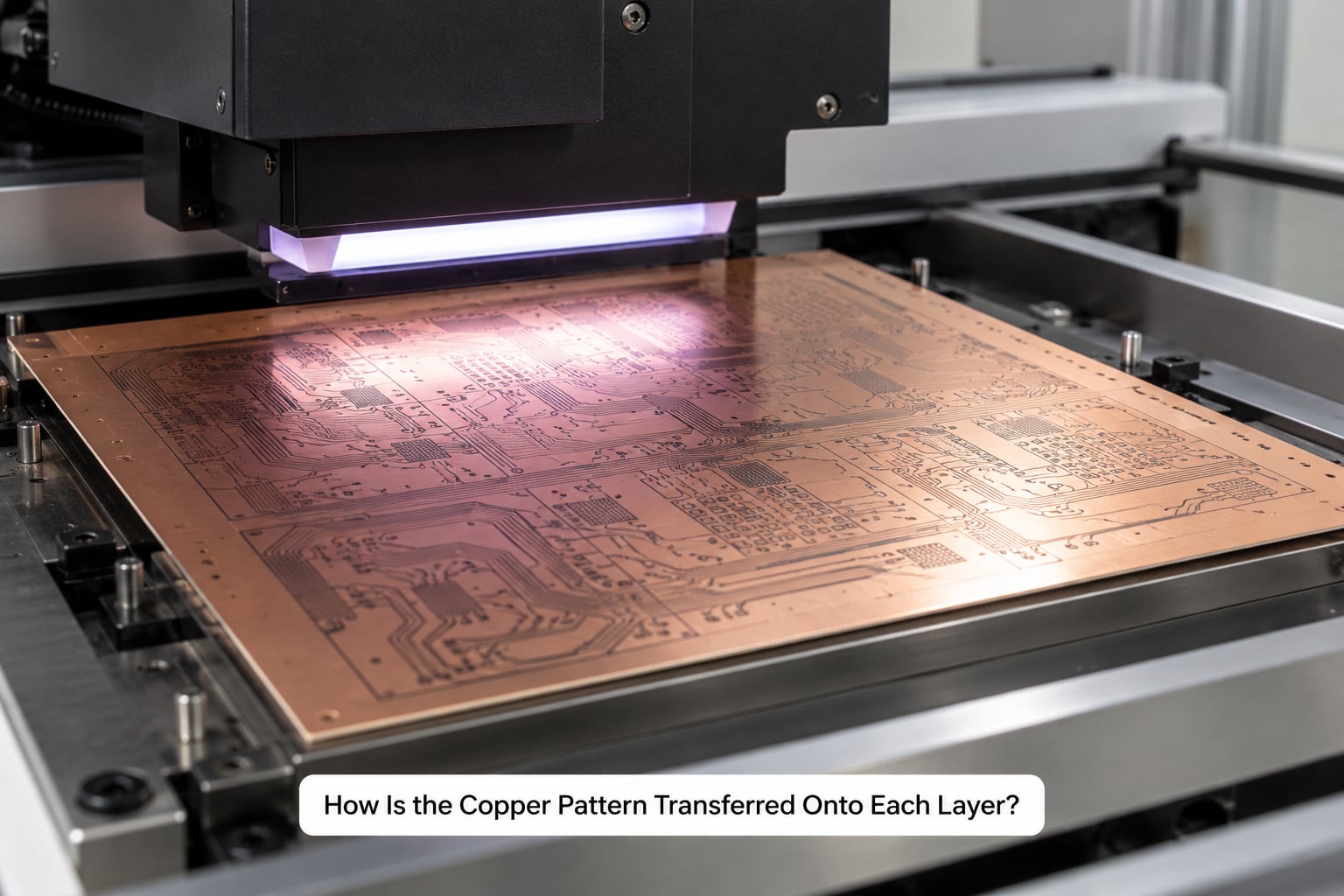
The pattern transfer is subtractive in most multilayer fabs: the whole copper surface starts as a sheet, a photosensitive resist is applied, artwork is exposed, and unexposed resist protects the copper you want while everything else is etched away. Liquid photoresist is common for outer layers because it conforms better, while dry film is preferred on inner cores because it gives predictable, even thickness.
On an inner layer the cycle runs: aqueous or mechanical cleaning, surface micro-etching and conditioning, dry film lamination, exposure by direct imaging or contact mask, alkaline or solvent development, cupric or ferric etching, resist stripping, then AOI. The pattern is checked before the core ever goes near a press.
Outer layer imaging is the same idea with a different tool. Because the finished surface already carries plated barrels and a textured or untexted surface, it is cleaned, conditioned, and either dry filmed or directly imaged by laser, then developed and selectively etched.
| Method | How it works | Where it fits | Trade-off |
|---|---|---|---|
| Subtractive, contact mask | Artwork is exposed through a glass or film mask onto dry film | Legacy inner layer work, very high volume simple layers | Mask changes cost, resolution limited by the mask |
| Subtractive, laser direct imaging | Film is exposed directly from Gerber data by laser | Most modern inner and outer layers | Needs fine line capability, well understood process |
| Semi-additive | Thick resist is plated up, then resist stripped to leave the features | Fine-pitch and higher copper weight features | More chemistry, harder to control for very wide features |
| Additive and build-up | Copper is deposited only where the resist defines, with dielectric laser-drilled between builds | HDI, 1+N+1 and 2+N+2 constructions, fine-pitch BGA escape | Multiple lamination cycles, higher cost per panel |
How Are the Layers Aligned and Bonded Together?
Alignment is the step that decides whether a stack survives. The factory loads cores, prepreg cut slightly oversized, and copper foil into a fixture that locates each sheet with tooling pins and a fixed reference origin, so layer to layer offset is held to a few tens of microns rather than millimetres.
The press then does the actual bonding. Prepreg is resin-impregnated fiberglass that is not fully cured; under heat it softens, flows into the surface of the core and copper, wets out the copper texture, and then cross-links as the cycle completes. Typical press profiles run from about 150 to 200 degrees Celsius with a controlled ramp on the order of 2 to 5 degrees Celsius per minute, pressure near 2 to 3 MPa, and a hold long enough to reach full gelation.
The ramp rate matters more than most buyers expect. Push the temperature too fast and the resin cannot keep up with the expanding glass, so the panel bows. Hold too long and the resin over-flows, which thins the dielectric and shifts impedance. A press cycle is also where the board picks up most of its thickness tolerance, often within plus or minus 8 to 10 percent of target before final routing.
| Operation | What changes | What stays fixed |
|---|---|---|
| Press cycle | Separate cores, prepreg, and foil become one solid panel; resin flows and cures | Copper artwork stays etched and isolated; nothing is electrically connected yet |
| Drilling | Holes pass through the full finished thickness | Copper layers and their artwork |
| Plating | Barrel copper grows inside the holes and on the outer surface | Inner layer artwork, which is protected by resist and tenting |
| Outer layer etch | Excess surface copper is stripped away | Inner layer artwork and the plated barrels |
Copper stays electrically isolated through lamination. Nothing connects the layers until the drilling and plating stages, which is why a delamination or a resin-filled hole shows up later rather than at the press.
How Are Vias and Other Holes Formed?
Through-holes and most blind or buried holes are drilled with tungsten carbide or diamond-coated bits on a numerically controlled drill. A laser, usually CO2 for the dielectric and UV for fine copper features, handles microvias and the smallest blind holes where a mechanical bit would either wander or break.
Four dimensions govern whether a hole is manufacturable: finished diameter, drill size, plating thickness, and aspect ratio. Aspect ratio is hole depth divided by hole diameter. A 0.2 mm hole through a 1.6 mm board is a ratio of 8 to 1, which is routine; a 0.1 mm hole through the same board is 16 to 1 and needs tighter process control, because plating solution has to reach the bottom of the barrel and fresh copper must exchange with depleted solution.
Plated holes are cut 1.4 to 2.0 mils undersize depending on the design’s copper weight, then plated to full size. That compensation is why a finished 12 mil pad with a 7 mil drilled hole is normal, and why the drill chart and copper data must be released together. The annular ring, the copper remaining between the barrel and the pad edge, is the tolerance everyone measures first, because it is what carries mechanical stress and current.
Backdrilling is a secondary operation that reams away the copper stub left on the back of a blind via or on a through-hole. It matters for high-speed links where a stub resonates, and it adds a full tool set and a second pass through the panel. Non-plated holes are drilled larger and left uncoated, usually for mounting or alignment, and they must be called out separately in the drill file.
Sequential lamination fills the space between plain multilayer and true HDI. L1 and L2 plus a core is drilled, plated, and pattern plated, then a dielectric is added by laser, then the next level is built and the cycle repeats. It is the standard route for fine-pitch escape on a modern BGA where through-hole microvia pitch would not fit.
Which via type to use
| Via type | Where it starts and stops | How it is made | Trade-off |
|---|---|---|---|
| Plated through-hole | Outer layer to outer layer | Mechanical drill, then plate the full barrel | Simple and cheap, but it consumes routing area on every layer it passes |
| Blind via | Outer layer to an internal layer | Mechanical or laser drill to a set depth, then plate | Saves inner routing area, adds a depth target the drill must hit |
| Buried via | Internal layer to internal layer | Drilled and plated inside a sequential lamination cycle | Invisible from outside, requires at least one extra lamination cycle |
| Microvia | One build-up level to the next | Excimer or CO2 laser on a dielectric film | Very fine pitch, low resistance, high cost per board |
| Stacked microvia | Two or more levels of microvia in line | Repeated laser dielectric and plating cycles | Reaches deep inside fine-pitch BGA, adds layers and cost for every extra build |
Two via-related decisions come up on almost every design review. First, keep a mechanical drill bit in a small enough diameter to hold its position on a thick panel, which is why microvias need a laser. Second, decide early whether a high-speed design can live with a via stub. Backdrilling removes the stub, but it leaves a non-plated hole, so the design has to be checked for that.
How Is Copper Added Inside the Holes?
Plating cannot start on resin, so the hole wall has to be prepared. Desmear removes the resin and glass debris left by drilling, usually with a permanganate or plasma process. Chemical activation or micro-etching strips a thin layer of copper to expose fresh metal, and an oxidation step prevents it from re-tarnishing.
Then electroless deposition lays a thin, uniform copper film over the entire hole wall and surface without any electrical connection. That seed layer is what makes the barrel conductive enough for the electrolytic step that follows.
Electroplating in a copper sulfate bath builds the barrel and the surface traces up to the target copper weight, typically 1 oz or 2 oz. Horizontal and vertical panel plating are both common, and pulse plating is used on high-aspect-ratio work because reversing the current sweeps out bubbles and loose copper from the narrow barrel.
How Are Outer Layers Patterned After Plating?
After plating, the surface is a uniform copper sheet with barrels standing proud of it. Patterning turns that sheet into artwork. The surface is cleaned and conditioned, dry film is laminated or the panel is coated with liquid photoresist, the artwork is exposed, the resist is developed, and the exposed copper is selectively etched away.
The sequence is deliberate. Until through-hole plating is complete there is no reliable connection between layers, so the pattern cannot be finished earlier. The inner artwork is protected throughout by plating resist and, where tenting is specified, by the dry film that stayed on the surface during plating.
Copper balancing comes after the etch, where the outer layers do not carry the same weight and the board would sit unevenly in an assembly. Plating thieving and copper balancing add a light, patterned layer of copper or film so the finished stack is symmetric, which controls warpage through reflow. The finished artwork is then compared to the source data by AOI and, on high-reliability work, by netlist comparison after plating.
What Finishes and Surface Treatments Are Applied?
Exposed copper oxidises and does not solder well, so a finished board needs a protective and solderable surface. The choice trades solderability, flatness, wear resistance, cost, and shelf life against each other, and it should follow the assembly process, storage conditions, and the finish the component library was qualified against.
| Finish | How it is applied | Solderability | Flatness | Typical fit |
|---|---|---|---|---|
| HASL, leaded | Dip in molten solder alloy | Excellent, keeps parts wettable through storage | Uneven; adds up to a few mils | Through-hole assembly, cost-sensitive work |
| HASL, lead-free | Dip in lead-free alloy | Good, but oxidises faster in storage | Uneven, similar to leaded | RoHS-compliant through-hole work |
| ENIG | Electroless nickel then immersion gold | Very good and highly stable | Very flat | Fine pitch, wire bonding, RF and medical |
| ENEPIG | ENIG with a thin palladium layer under the gold | Very good, resists black immersion gold | Very flat | High-reliability and fine-pitch applications |
| Immersion silver | Chemical displacement of tin | Good | Flat | Lead-free assemblies needing flatness |
| Immersion tin | Chemical displacement of silver | Good, but whisker-prone in some conditions | Fairly flat | RoHS work with cost limits |
| OSP | Organic surface protectant on bare copper | Good but not for high-temperature exposure | Flat | Cost-driven, lead-free, limited rework |
| Hard gold | Gold over a nickel strike, electrodeposited | Wear resistant rather than optimised for soldering | Flat on a controlled thickness | Edge connectors and contact pads |
Finishes are applied after solder mask has been cured and developed, with openings left where pads must remain bare. Ordering matters: the mask goes on before the finish, so the chemistry only touches exposed copper.
Mask and legend are part of the same finishing sequence. Solder mask is a screen-printed or liquid-sprayed epoxy that is exposed through artwork, developed to open the pads, and cured by UV or thermal means. Legend and silkscreen ink is printed on top and cured the same way, and the two colours must be checked for pad clearance because a legend square sitting on a pad is an assembly defect, not a cosmetic one.
How the panel is cut into boards
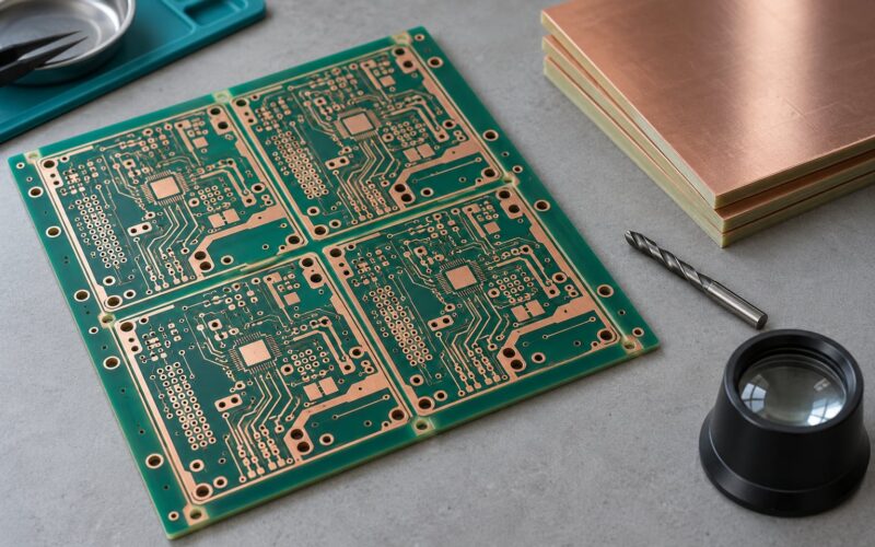
Depanelization is the last mechanical step. V-cut scoring runs a diamond wheel along a straight line close to the edge and then flexes the panel, which is fast and cheap but leaves a chamfered, slightly stressed edge and only works on straight boundaries. Routing mills a continuous path with a small end mill for any outline, including curves, at the cost of a wider, less precise edge. Laser cutting is used for very small or very dense panels, and punch-and-punch tooling is still the fastest option when the design uses a simple rectangular outline and a high volume.
Whatever the method, a routed edge exposes the glass and resin fibre ends. That is normal, but it is where moisture enters, so boards meant for damp environments get a coating or a sealed option.
How Is a Completed Multilayer PCB Inspected and Tested?
Final inspection catches what earlier steps could not, because only the finished board shows the whole stack interacting. Dimensional measurement checks thickness, hole sizes, and annular rings against the drawing. AOI compares copper, mask, and legend artwork to the source data, and X-ray inspection looks at internal structures, via barrels, and tented holes that optical inspection cannot see.
Electrical testing is the last gate. A flying probe makes contact with test points and pads to find opens, shorts, and wrong resistance on a bare board. A fixture test uses a purpose-built jig for high volume production, since a bed of nails is faster once a design is in steady production. A netlist comparison test checks the full connection list, and in-circuit test happens after assembly, not on the bare board.
Reliability work goes further. Microsection analysis cuts a hole in half under a microscope to measure the barrel, resin fill, and copper distribution. Boundary scan and burn-in suit complex digital designs, and accelerated tests such as thermal cycling or high temperature and high humidity exposure reveal conductive anodic filament, a failure mode where copper ions migrate under moisture and bias and grow a conductive bridge between conductors.
| Defect | Typical root cause | How it is found |
|---|---|---|
| Open circuit | Etch loss on a fine trace, via misregistration, plating void in a barrel | Flying probe, netlist test, X-ray of the via |
| Short circuit | Residue between traces, plating bridge, inner antipad missing | AOI, netlist test, cross-section |
| Insufficient copper | Under-plated barrel, etched-away pad, thin final copper weight | Microsection, X-ray density check |
| Resin-filled hole | Desmear incomplete after a high aspect ratio laser or mechanical hole | Electrical test, cross-section |
| Delamination | Contaminated surface, insufficient resin flow, moisture in the stack | Microsection, cross-section, thermal stress test |
| Misregistration | Stack alignment drift, panel movement, foil placement error | Inner layer AOI, microsection |
| Warpage | Unbalanced copper or dielectric, uneven drilling, uncontrolled reflow profile | Out-of-plane measurement on a tester |
| Impedance out of tolerance | Dielectric thickness drift from resin flow, or a different laminate lot | TDR impedance measurement, cross-section |
If you want to confirm a board you have received, the practical sequence is: read the fabrication drawing and the layer count from your data, count the visible mask and legend layers, run an X-ray to count buried copper features, and cut a corner on a sacrificial sample for a cross-section. Only the cross-section gives you real dielectric thickness, real copper weight, and a true read on annular ring. Hobbyists on machining forums point out the same thing from the other direction: the real limit on home-built multilayers is registration across repeated inner cycles, not the ability to etch a thicker board.
Frequently Asked Questions
Are multilayer PCBs stronger than double-sided PCBs?
Not meaningfully in bending stiffness, which is set mostly by board thickness, material, and copper distribution. A four-layer board with a thin core can be weaker than a thick double-sided board. What multilayer changes is resistance to vibration and warpage, because balanced inner copper keeps the neutral axis in the middle and the stack stays flat through reflow.
What is the minimum number of layers for a multilayer PCB?
Three copper layers is the practical minimum, and most fabricators treat three or more as a multilayer build. Four layers is far more common because it gives a signal, ground, power, and signal arrangement with a continuous return path. A true three-layer board is asymmetric and tends to bow during the press cycle and reflow, so buyers rarely choose it when four is affordable.
How are the layers inside a PCB connected?
By vias. A plated through-hole runs the full board thickness and connects every layer it passes. A blind via connects an outer layer to an internal one, and a buried via connects two internal layers without touching the surfaces. A microvia is a small laser-drilled via used in build-up stacks. Each barrel is electroplated so the copper wall itself carries the connection.
What is the difference between a four-layer PCB and a four-layer build-up PCB?
A conventional four-layer board has two outer copper layers and two inner layers reached by drilling through the full thickness. A four-layer build-up has a two-layer core with microvias added on each side, giving four effective routing layers with lower via resistance and much finer escape pitch. The build-up route costs more and needs repeated lamination cycles.
How thick can a multilayer PCB be?
Standard multilayer designs run from about 0.8 mm up to roughly 3.2 mm before thickness becomes a real engineering problem. Backplanes and high-layer-count boards go thicker, sometimes 5 mm or more, using heavy copper and stepped structures to control sag. Past that, warpage, drilling chip evacuation, and plating uniformity force designs toward metal-core or a modular approach.
Start by fixing the five inputs that drive everything downstream: a verified stackup with dielectric thicknesses, impedance targets with tolerances, a drill scheme that marks plated, non-plated, blind, and buried holes, a surface finish matched to the assembly process, and a defined test method. Release those as one consistent package and the rest of the flow runs without clarification loops.