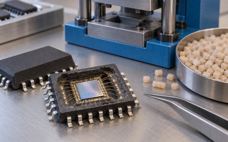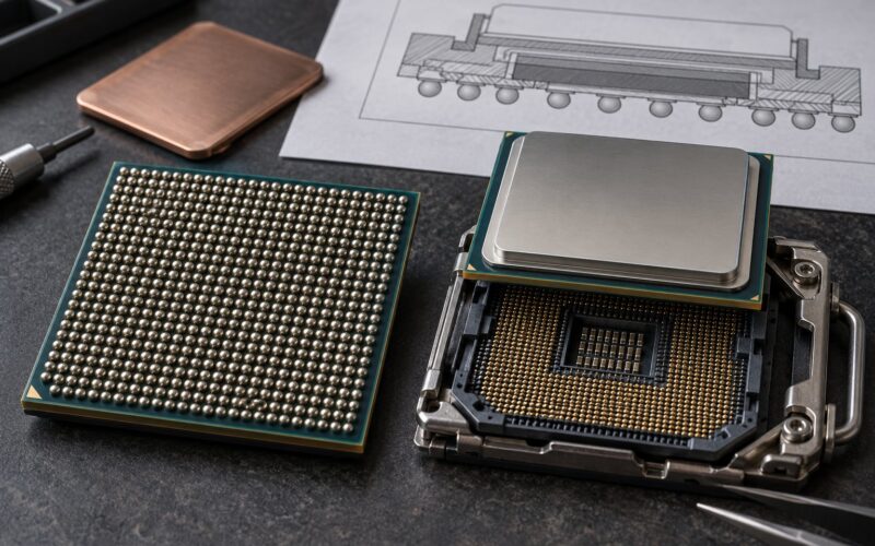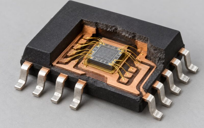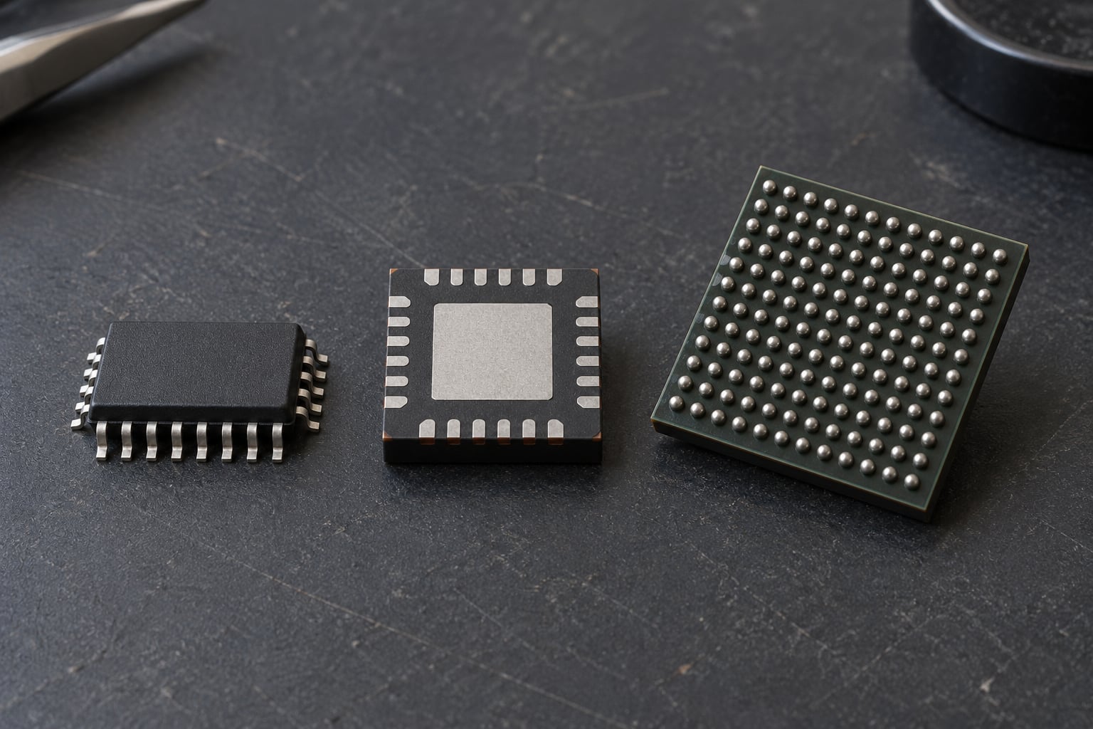
SOIC uses gull-wing leads on two sides, QFN puts connection pads and a central exposed thermal pad flush against the underside of the body, and BGA arranges solder balls in a two-dimensional grid. That single choice — how the connection leaves the die — is what separates their size, heat path, assembly method, inspectability and cost. This SOIC vs QFN vs BGA package comparison covers all three side by side so you can pick one for the board you are actually building.
If you are hand-soldering a first board, SOIC wins outright because the joints are visible and a 1.27mm pitch is easy on an iron. If the design dissipates more than about a watt or has to fit in a tight enclosure, QFN is the step up, provided the exposed pad gets a proper via array. If the pin count passes a hundred or the signals cross several hundred megahertz, BGA is the only realistic option, and it comes with reflow, X-ray and a specialist rework station attached.
Package choice is close to irreversible. The footprint, the layer count, the inspection plan and the debug strategy are all locked in at schematic stage, so a wrong call means a respin rather than a component swap.
Table of Contents
- SOIC vs QFN vs BGA Package Comparison at a Glance
- What Are SOIC, QFN, and BGA Packages?
- How to read a package drawing, pin 1, pitch and the exposed pad
- How Do SOIC, QFN, and BGA Packages Differ in Size and Pin Count?
- Which Package Has Better Thermal Performance?
- How Do Solderability and PCB Assembly Compare?
- What About Cost, Availability, and Prototyping?
- Which Should You Choose?
- Frequently Asked Questions
- What is the difference between SOIC, QFN and BGA packages?
- What is the difference between SOP and SOIC packages?
- What is the difference between QFP and QFN packages?
- Can I hand solder fine-pitch QFP or QFN packages?
- What PCB technology do I need for different BGA ball pitches?
- Can I swap a package without changing the PCB?
- Conclusion
SOIC vs QFN vs BGA Package Comparison at a Glance
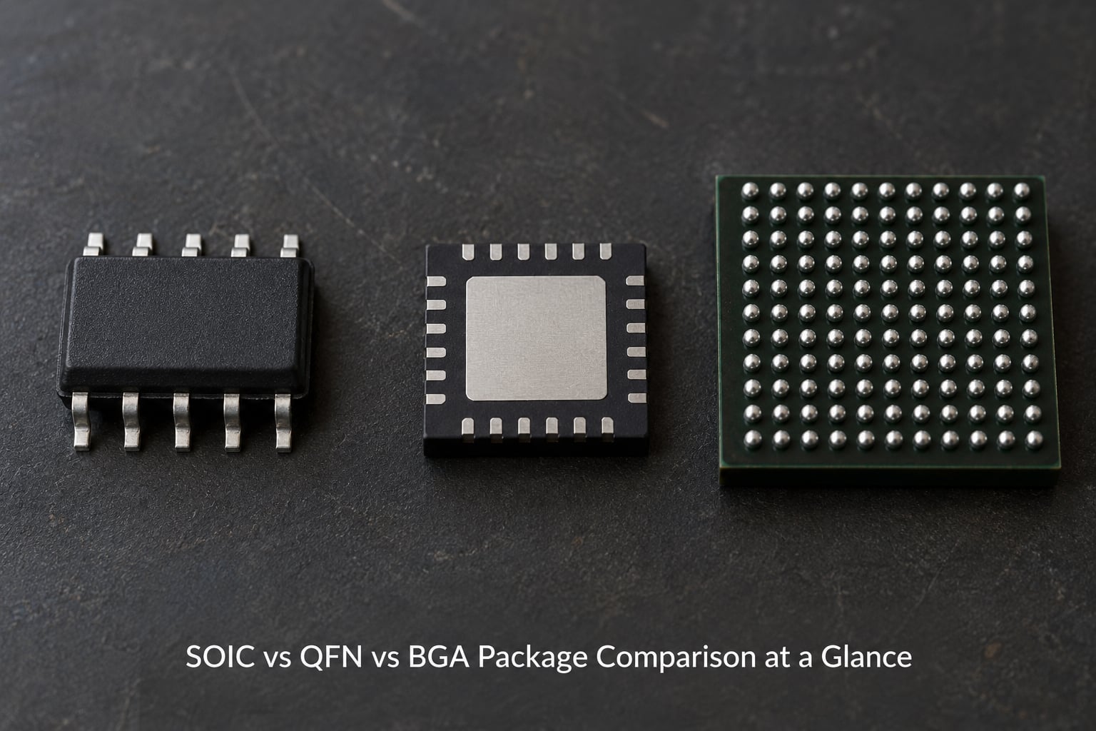
| Attribute | SOIC | QFN | BGA |
|---|---|---|---|
| Connection style | Gull-wing leads, two sides | Flush pads on the underside, no protruding leads | Solder ball array on the underside |
| Typical pitch | 1.27mm, 0.65mm on SSOP | 0.4mm to 0.65mm | 0.3mm to 1.27mm ball pitch |
| Typical pin count | 8 to 28 | 8 to 128 | 100 to 2500 and beyond |
| Body size range | 4.9mm to 7.5mm wide | 2mm to 12mm square | 5mm to 45mm square |
| Thermal path | Through the leads, long and narrow | Direct through the exposed centre pad | Through the ball array and substrate |
| Junction-to-ambient (theta-JA) | 80 to 150 C/W | 25 to 40 C/W with a via array | 20 to 30 C/W for a mid-size array |
| Assembly | Basic SMT line, or a bench iron | SMT with controlled paste volume | SMT with profiled reflow |
| Optical inspection | Straightforward, joints visible | Not possible, joints hidden under the body | Not possible, joints hidden under the body |
| X-ray needed | No | Usually | Always |
| Rework | Joint-by-joint repair on the bench | Usually full removal, then re-inspect | Specialist hot-air station plus reballing |
| Bench hand soldering | Easy and routine | Possible with hot air and applied paste | Not realistic |
| Typical applications | Op-amps, comparators, LDOs, gate drivers | Wireless SoCs, MCUs, power converters | DDR memory, FPGAs, application processors |
The table makes the pattern plain: SOIC buys you visibility and simplicity, QFN buys you density and a short heat path, and BGA buys you pin count and signal performance at the price of everything you can no longer see. Every other difference follows from that one row at the top.
What Are SOIC, QFN, and BGA Packages?
All three are surface-mount IC packages, and all three do the same three jobs: protect the die, bring its connections out to the board, and move heat away from the silicon. Only the geometry of the connection differs.
SOIC means Small Outline Integrated Circuit. Leads exit from the two long sides of the body, bend down, and land on pads you can see with the naked eye. Sizing is generous, the pitch is 1.27mm on the standard body, and pin counts sit in the 8 to 28 range with a practical ceiling around there.
QFN means Quad Flat No-Lead. There are no protruding leads at all. The connection pads sit on the underside of the body, and a larger metal pad in the middle doubles as the heat path to the board. A common part to know is the ESP32, which ships as a QFN-48.
BGA means Ball Grid Array. Solder balls cover the entire underside in a grid, so terminals are distributed across the area of the package rather than around its perimeter. This is the package family behind DDR5 and LPDDR4X memory and behind most FPGAs and application processors.
One naming trap worth clearing early: people use SOP and SOIC interchangeably, and they are not the same part. JEDEC withdrew SOP years ago, and the name now survives mainly in distributor listings. The modern equivalent is the SOIC family — plus its narrower siblings SSOP (0.65mm pitch) and TSSOP (0.65mm pitch, thinner body) — and a distributor marking a chip SOP is usually describing a small-outline gull-wing part.
QFP is the fourth family you will meet constantly, usually because search results pair it with QFN. A QFP is a Quad Flat Package: gull-wing leads on all four sides, no exposed pad. It is the bridge between SOIC and QFN — more pins than a SOIC, still-visible joints, but more board area than a QFN. A QFN gets its density advantage by removing the leads entirely, which is also what makes the joints invisible.
How to read a package drawing, pin 1, pitch and the exposed pad
Every outline drawing carries the same handful of cues. Pin 1 is marked by a dot, a chamfered corner, a half-circle notch, or a lead-1 chamfer, and it is the anchor for counting every other pin in the direction the datasheet specifies. Pitch is the centre-to-centre spacing between terminals. On a QFN or BGA, an EP or EPD label marks the exposed pad, and its pitch is calculated separately from the signal terminals because it sits on a different, often larger, grid. Standoff height is the gap between the package body and the board, and the IPC-7351 land pattern tells you the pad size, spacing and courtyard that the footprint generator should use.
The rule I would not break: use the manufacturer’s recommended land pattern from the datasheet rather than a generic library footprint. A generic QFN-48 footprint is a guess, and a wrong guess shows up weeks later as bridging or open joints that are invisible without X-ray.
How Do SOIC, QFN, and BGA Packages Differ in Size and Pin Count?
A SOIC-8 occupies about 4.9mm by 3.9mm of board. A QFN-24 at 0.5mm pitch covers roughly 4mm by 4mm while carrying three times the terminals, and a BGA-256 fits more than twenty times the connections into a similar footprint by using the whole underside.
The reason is a density ladder. SOIC puts terminals on the perimeter, so available terminals grow with edge length and nothing else. QFN moves them to the underside but keeps them on a perimeter ring. BGA fills the entire area, so terminals scale with the square of the body size rather than the square root. That is the whole reason a 240-ball part exists and a 240-lead SOIC does not.
Size has a cost, and it is routing. SOIC leads are long, roughly a millimetre of trace per side before you reach the first escape, which makes dog-bone fanout easy and signal integrity forgiving. QFN at 0.5mm pitch leaves a very short escape, so traces have to go directly to vias in most directions. BGA at 0.4mm or finer cannot escape to an inner layer at all without a microvia right in the pad.
The practical crossover is easy to name. Below about 40 pins and under a watt, SOIC is usually sufficient. Somewhere between 40 and 100 pins, or once the part dissipates more than a watt, QFN starts to win on space and heat. Past roughly 100 pins, or when edge lengths above 500MHz are involved, BGA is the only option left, and the board has to grow up around it.
Which Package Has Better Thermal Performance?
QFN and BGA beat SOIC on heat, and the gap is large — roughly four to five times better for the same die in a comparable footprint. The reason is path length. A SOIC lead is long, thin and made to carry signal current, not heat, so heat has to travel up a conductor designed for something else. A QFN exposed pad is a solid metal area bonded directly to the die, sitting millimetres from the board. A BGA spreads heat through a large ball array into a substrate built for it.
| Package variant | Typical theta-JA | Rough power ceiling |
|---|---|---|
| SOIC-8 | 110 to 150 C/W | Under 0.5 W |
| SOIC-16 | 80 to 100 C/W | Around 0.6 W |
| TSSOP-20 | 90 to 120 C/W | Around 0.5 W |
| QFP-100 | 35 to 50 C/W | Around 1.5 W |
| QFN-32 with exposed pad | 25 to 40 C/W | 2 to 4 W |
| BGA-256 | 20 to 30 C/W | 4 to 8 W |
| FCBGA-1000 | 8 to 15 C/W | Well above 10 W |
Two numbers matter more than the package name. First, above roughly one watt an exposed pad stops being optional and SOIC comes off the table — the thermal maths simply will not work through those leads. Second, a QFN number is meaningless without a via array. A datasheet theta-JA for a QFN assumes a specific via count, copper pour area and layer count, and a bare footprint on thin two-layer FR4 can land three or four times worse than the datasheet figure.
Design the array before the footprint. A 3×3 to 5×5 grid of 0.3mm to 0.4mm vias on roughly 0.45mm to 0.6mm centres under the exposed pad is the usual starting point, tie the pad to a copper pour on the opposite side, and fill or cap the vias with paste so solder cannot wick away from the joint.
How Do Solderability and PCB Assembly Compare?
Hand soldering is where the three separate most sharply, and where the advice on the first page of search results contradicts itself. Here is the straight version.
- SOIC: yes, with a normal iron. A 1.27mm pitch is comfortably solderable. Even a 0.65mm SSOP is routine with flux and steady heat.
- QFP: yes at 0.5mm pitch and above, using drag soldering and good flux. Below 0.5mm it stops being pleasant.
- QFN: only with hot air and deliberate paste. Place paste with a syringe or stencil, heat the whole body evenly, and let surface tension seat it. The joints cannot be checked or touched afterwards.
- BGA: not with an iron. You cannot see a single joint, and the balls are under the part. This needs reflow.
On the line, QFN has its own well-documented failure mode: voiding in the exposed pad. Too much paste, one solid centre aperture, or unfilled vias that swallow solder all produce a hollow joint, and the joint looks acceptable while the part runs hot. IPC-7093 is the reference here, and the common acceptance limit used for bottom-termination components is 25 percent voiding in the thermal area. Design around it with a windowed or crosshatched centre aperture rather than one solid opening, keep total aperture coverage around 50 to 70 percent, and specify filled or capped vias in the pad.
Inspection follows directly from geometry. SOIC and QFP leads stick out where light can reach them, so automated optical inspection reads the joint directly and solder paste inspection can verify the print before placement. QFN and BGA hide every joint under the body, so optical inspection can confirm placement and orientation and nothing else. X-ray radiography is the only way to see a bridging or head-in-pillow defect underneath, which is why bottom-terminated parts trigger X-ray coverage on essentially every serious assembly.
Rework inherits the same wall. A single SOIC joint can be re-flowed with an iron. A failed QFN is normally removed whole, cleaned, replaced and re-inspected, because you cannot confirm the repair without X-ray. A failed BGA needs a dedicated removal station to avoid board damage, and the replacement often needs reballing before it will go back down.
The principle I keep coming back to: a package that saves board area but cannot be verified or repaired on your equipment is not a saving. It is a deferred problem with a better marketing story.
What About Cost, Availability, and Prototyping?
Silicon cost and assembly cost are separate lines, and most package-cost arguments confuse them. The same die in a different outline is usually a small difference in price, sometimes less, because the bill of materials inside the package is unchanged. The real delta shows up in what the assembly house has to do with it.
A SOIC is placed and reflowed like any other surface-mount part, inspected optically, and repaired with hand tools. A QFN adds paste-volume control, a specific stencil design and X-ray coverage. A BGA adds profiled reflow, mandatory X-ray, more board layers for escape routing, a shorter rework chain, and the largest per-board adder at low volume. The Electronics Stack Exchange thread on package cost during assembly exists because nobody publishes these numbers per package; the practical takeaway is to ask your assembly house for a per-position quote broken down by package, because the answer will not match the component price list.
Availability is the quieter risk. Analog and general-purpose parts — op-amps, LDOs, interface chips, most small MCUs — ship in SOIC and QFN from multiple manufacturers, and dropping one vendor usually means changing one part number. High-end SoCs and DDR memory are BGA-only, often with a single qualified source, which turns a routine second-source exercise into a requalification project.
That is also the strongest argument for the migration pattern. Prototype in the package you can actually build, prove the design works, then move to the finer production package before the design is frozen. The recurring view in r/PrintedCircuitBoard and r/soldering threads is exactly that: use the accessible package while you are still changing things.
Which Should You Choose?
Start from what your build environment can handle, not from what is technically optimal, because the optimal package for a design is frequently the one your shop cannot assemble or inspect.
| If your priority is | Choose | Because |
|---|---|---|
| Soldering on a bench, learning | SOIC, or DIP before that | Visible joints, forgiving pitch, iron and flux only |
| Prototypes you may rework | SOIC or QFP | Failures can be found and fixed without X-ray |
| Small enclosure | QFN | Same function in roughly half the area |
| Over 1 W dissipation | QFN or BGA with an exposed pad | SOIC leads cannot carry the heat away |
| Over 100 pins | BGA | Perimeter packages run out of edges |
| Signals above roughly 500 MHz | BGA | Short, stubless interconnect keeps inductance under control |
| Field service or repair | SOIC or QFP | Joints stay accessible for years |
| High volume with mature line capability | BGA | Inspection and rework costs amortise across the run |
| Lowest BOM risk | SOIC or QFN | Multiple sources, longest lifecycle support |
The decision path, in order. Check what you can assemble, inspect and repair — that alone often decides it. Then apply the thermal budget: above about a watt, exposed pad or nothing. Then check pin count against the family ceiling. Then check signal speed against package inductance. Only after all four come back clean should you look at cost, and by then it is usually a rounding error next to the rework risk.
One more practical detail from the forums: QFN packages give almost no visual orientation cue, so centroid and rotation data errors are a common and expensive failure. Take the pick-and-place data from the manufacturer’s own library rather than drawing your own, and check the centroid for the specific part number on the assembly drawing.
Frequently Asked Questions
What is the difference between SOIC, QFN and BGA packages?
SOIC connects with gull-wing leads on two sides at roughly 1.27mm pitch, so joints stay visible and hand-solderable but pin counts top out near 28. QFN puts pads flush on the underside with a central exposed thermal pad at 0.4-0.65mm pitch, giving better heat transfer and a much smaller footprint at the cost of hidden joints. BGA fills the whole underside with a solder ball array for pin counts from a hundred upward and the shortest possible electrical path, but every joint needs X-ray to inspect.
What is the difference between SOP and SOIC packages?
SOP was the older JEDEC name for the small-outline package and was withdrawn years ago; the name survives mainly in distributor listings. SOIC is the current family name for the same general form factor, a plastic body with gull-wing leads on two sides. The families often overlap in practice, so the real check is the body width, lead pitch and pin count on the datasheet rather than the label on the listing.
What is the difference between QFP and QFN packages?
A QFP has gull-wing leads on all four sides and no exposed pad, so joints are visible and solderable with an iron, but it eats board area and runs hot. A QFN removes the leads entirely, putting pads on the underside and adding a central exposed pad, which makes it smaller and cooler but hides every joint. If you are on a bench without X-ray, stay with the QFP.
Can I hand solder fine-pitch QFP or QFN packages?
QFP at 0.5mm pitch and above is hand-solderable using drag soldering and quality flux. QFN is possible with hot air: apply solder paste with a syringe, heat the body evenly, and let surface tension seat the part, but you cannot inspect or touch the joints afterwards. BGA should not be hand-soldered with an iron at all, since no joint is visible and the array will not self-align reliably.
What PCB technology do I need for different BGA ball pitches?
A 1.0mm or 1.27mm ball pitch escapes comfortably to an inner layer on a standard four- to six-layer board. Around 0.8mm you generally need a six-to-eight-layer stackup with close pad-to-via spacing. Below 0.65mm, most designs move to HDI with microvias in the pad, because the escape trace no longer fits between balls. Below 0.4mm assumes laser-drilled microvias and a fine-line capability that sits with specialist fabricators.
Can I swap a package without changing the PCB?
Only rarely. SOIC, QFN and BGA have different body sizes, terminal layouts and pin numbering, so a footprint swap is a layout change, not a BOM change. The exception is a deliberate dual-footprint design, where the pads are laid out to accept two known package variants of the same die and the unused terminals are tied off. Even then the land pattern has to be drawn for both outlines from the start, and a change made afterwards means a new spin.
Conclusion
The rule is short. Use SOIC when you want to see and fix your joints, QFN when heat or board area is the binding constraint and your assembly can handle paste control plus X-ray, and BGA when pin count or signal speed leaves you no other option. Backing off one step is not failure; committing to a package your process cannot verify is what costs you a respin.
Before you lock the package, check five things: your required pin count, the board area you have, the worst-case dissipation, the assembly and inspection capability you actually have access to, and the manufacturer’s recommended land pattern. If those five agree, the package choice follows on its own — and the table at the top of this guide is the shortest way to settle it.