The PCB manufacturing process step by step is a fixed sequence of chemical, mechanical and optical operations that turns your design data into a physical bare board. The inputs are Gerber, ODB++ or IPC-2581 artwork, an NC drill program and an IPC-D-356 netlist; the output is a drilled, plated, masked, silkscreened and electrically tested printed circuit board, usually still attached to its production panel.
What the process does at every stage is straightforward: transfer, remove or protect material. A dry-film photoresist is applied and selectively hardened by laser direct imaging to define which copper survives. Alkaline develop and a chemical etch strip away everything unprotected. The defined layers are pressed together with prepreg in a lamination cycle, holes are drilled, and their walls are made conductive by electroless then electrolytic copper plating. Solder mask and a surface finish go on next, legends are printed, and the board is tested against the netlist before it is routed or V-scored out of the panel.
Ten stages get a board from a data file to a shippable part. The exact order and inspection points shift with layer count, copper weight, surface finish and fabricator, so treat what follows as the reference flow and confirm capability numbers with the shop before release. Every H2 and H3 here appears once; skip to What You Need if you want the input files first, or straight to Step-by-Step if the package is already assembled.
Table of Contents
- What You Need
- The PCB manufacturing process step by step at a glance
- Step-by-Step
- 1. Engineering Review and CAM Preparation
- 2. Material Selection and Board Preparation
- 3. Inner Layer Imaging and Etching
- 4. Lamination and Layer Alignment
- 5. Outer Layer Imaging, Plating, and Etching
- 6. Surface Finish and Solder Mask
- 7. Silkscreen, Routing, and Drill Processing
- 8. Electrical and Dimensional Inspection
- 9. Component Assembly and Soldering
- 10. Final Testing, Packaging, and Delivery
- Common Mistakes
- Frequently Asked Questions
- What files do I need to send a PCB manufacturer?
- Which file format is used for PCB manufacturing?
- How long does PCB fabrication take?
- What is the difference between PCB fabrication and PCB assembly?
- What electrical testing is done on a bare PCB?
- Are PCBs easy to manufacture as a beginner?
- How to Start a Reliable PCB Manufacturing Project
What You Need
Almost every delayed PCB order I have seen traced back to one thing: the release package was incomplete, so the fabricator was guessing. Put these files together before you send anything.
- Fabrication artwork in Gerber RS-274X or X2, or ODB++ / IPC-2581 if your shop prefers a single file.
- NC drill file with the tool table, plus a drill map or layer pair indicating plated versus non-plated holes.
- IPC-D-356 netlist used by the factory to build the electrical test program.
- Layer stack-up with material, dielectric thickness, copper weight and finished thickness, including any controlled impedance targets.
- Fabrication notes covering IPC class, surface finish, solder mask colour, minimum trace and space, and any special tolerances.
- Bill of materials and pick-and-place file only if you also want assembly.
- Approved test criteria such as the electrical test method and the documentation you expect to receive back.
Designers often encode these decisions as dedicated fabrication layers inside the Gerbers rather than a separate memo. It works, and shops read it, but a written note alongside the files removes every ambiguity about which layer carries which instruction.
The PCB manufacturing process step by step at a glance
Here is the whole sequence in one list, with the conditional stages marked so you can tell where a two-layer board leaves the multilayer path.
- Engineering review, DFM check and CAM preparation
- Material selection, panel cutting and board preparation
- Inner layer imaging, development and etching (multilayer and above)
- Lamination and layer alignment (multilayer and above)
- Drilling and deburring
- Electroless copper and outer layer imaging (multilayer metallization)
- Copper plating, tin plating, strip and final etch
- Solder mask application and cure
- Surface finish
- Silkscreen or nomenclature printing
- Electrical test, dimensional inspection and routing
- Assembly, in-circuit or functional test, packaging and shipment
The ordering conflict you will notice between sources comes from board type. A two-sided board drills before outer imaging because it has no inner layers to protect. A four-layer board builds and etches its inner cores first, laminates them, then drills through the bonded stack. Nobody is wrong; they are describing different flows.
Step-by-Step
The stages below follow the multilayer reference flow. Where a step does not apply to a simple two-layer board, that is stated rather than skipped, so you can use this as a checklist against any fabricator’s process sheet.
1. Engineering Review and CAM Preparation
The first stage converts your design intent into machine instructions. An engineer checks the Gerber set against the drill file and netlist, confirms layer count and stack-up, and looks for the errors that a CAM system will not catch on its own: a missing layer, an unterminated trace, a pad with no drill, a clearance that falls below the shop’s stated capability.
What a reviewer should confirm, specifically:
- The layer count in the artwork matches the stack-up you ordered.
- Every drill hit has a matching pad, and every pad has a matching hit.
- Minimum trace, space and drill sit above the fabricator’s published limits, with your own margin on top.
- Controlled impedance targets are stated as a tolerance, such as 50 ohm plus or minus 10 percent, not as a single number.
- Panelization requirements, tooling holes and fiducials are defined before anything is cut.
Most shops run a design-for-manufacture check here and send back a report. On r/PrintedCircuitBoard and r/Altium, designers describe the painful version of this: DFM feedback arrives after the order is placed, so the fix costs a respin instead of a comment. Ask for the DFM review explicitly before you authorize production.
2. Material Selection and Board Preparation
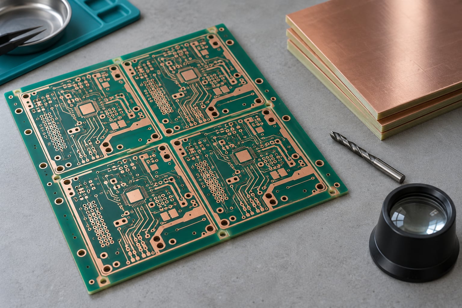
Raw laminate arrives as copper-clad FR-4, a core, or prepreg sheets that will be bonded later. The stack-up you approved determines the core thickness, the prepreg style, and the copper weight on each layer. FR-4 is the default; high-Tg FR-4, Rogers laminate for RF work, and polyimide for flex circuits are specified instead when thermal or RF behaviour demands it.
Panels are cut to the standard size the shop runs, and each board position is given its own tooling holes, fiducials and routing path. Copper on the panel edges that the profiler will cut through is deliberately removed so the router has a clean path.
Panels are then cleaned and degreased, handled with gloves, and identified with a job number and lot code. Material identity is not paperwork for its own sake: traceability back to a resin batch is what makes a thermal reliability failure investigable years later.
3. Inner Layer Imaging and Etching
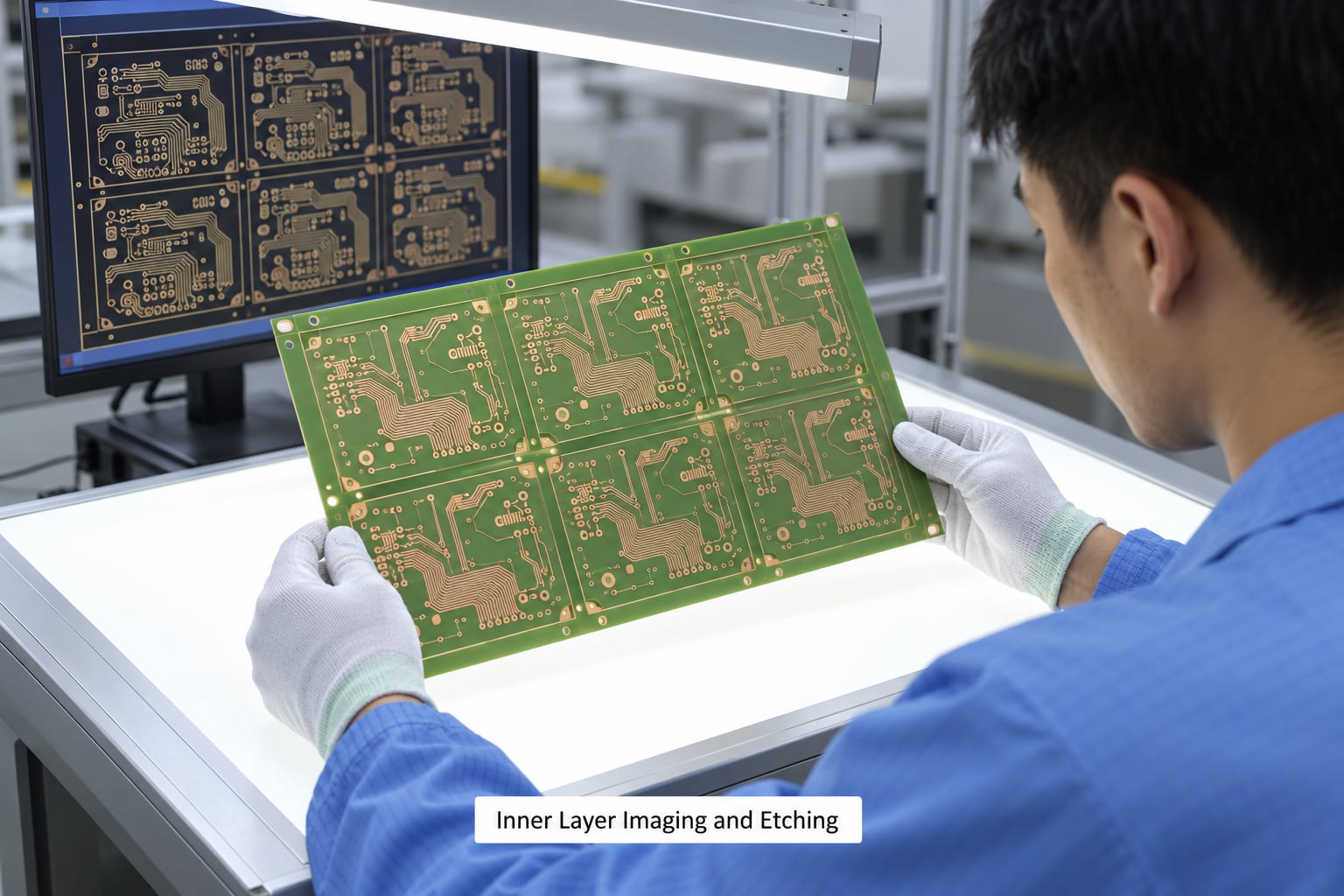
Each inner layer starts as a core with copper on both faces. Dry-film photoresist is laminated onto the surface, and laser direct imaging exposes only where copper should remain. The panel moves through an alkaline developer, which removes unhardened resist, then into an ammoniacal etchant that dissolves the bare copper. The exposed resist is stripped, leaving the trace pattern bonded to the core.
Automated optical inspection follows while the layer is still protected, so a broken trace or a short is caught before another sheet is stacked on top of it. An optical punch then creates registration holes, and every later layer aligns to those holes. That is why alignment matters so much here: each registration error of a few microns accumulates across the stack.
On multilayer boards the bare copper is also treated with an adhesion promoter or oxide process at this point, so the next bonding or plating step grips properly. Skipping it is a common cause of inner layer peel and delamination failures.
4. Lamination and Layer Alignment
The prepared cores, copper foils and prepreg sheets are stacked in the exact order the stack-up specifies and bonded in a heated press under controlled pressure. The resin in the prepreg flows to fill the gaps, then cures into a single solid slab. Some shops run a hot press cycle followed by a cold press cycle; the second step improves flatness.
Registration is the thing being controlled here. All layers align to the tooling and registration pins, and the press cycle is chosen so the finished thickness lands on target after the material contracts on cooling. Fabricators quote a scaling factor per material and thickness so the CAD data can compensate for shrinkage before release.
After bonding, the panel is inspected for voids, resin-filled gaps, delamination at the interfaces and warpage across the panel. A board that is out of flat here will cause problems later, at drilling and at reflow.
5. Outer Layer Imaging, Plating, and Etching
The bonded panel goes to the drill operation. X-ray target registration looks through the laminate to find the centre of each hole on the drill hit list, because the copper layers no longer line up optically with the artwork after lamination. Then mechanical drills, or laser drills for very small holes, cut through the stack. Carbide tooling wears during the run, so hole diameters are measured and compensated rather than trusted across a whole panel.
Holes are deburred afterwards, then desmear and etch-back remove the resin and loose fibres left on the wall by drilling. This step matters for a reason that is easy to miss: glass and resin fibres standing proud inside a hole can stop the plating chemistry from reaching the wall evenly, which produces a via that looks plated and is not.
Electroless copper then deposits a thin seed layer over the exposed hole walls and outer copper by an autocatalytic reaction, with no external current involved. A palladium-based catalyst activates the surface first. From there the outer layer is imaged with dry film, and electrolytic copper plating builds the traces, pads and barrel plating inside every hole to the required thickness.
Vias and plated through-holes share that plating step. A via is a small plated hole joining layers with no component attached; a plated through-hole is a plated hole that takes a pin. The annular ring is the copper ring around a hole; if plating is thin or the drill wanders, the ring breaks and the connection fails. Blind and buried vias are plated but not open at one or both ends, which means the plating process has to be controlled from both faces of the panel.
6. Surface Finish and Solder Mask
Solder mask is an LPI liquid applied through a screen, exposed, developed and cured. It covers everything except the pads and vias you want exposed, and it defines where a component’s solder will actually land. Most mask is green because that pigment blocked the deepest UV exposure of the photo initiators available when the process was commercialised. The colour is nearly free to change, and white mask under blue LEDs is a common choice.
Surface finish goes on the exposed copper to protect it, keep it solderable and give the pads a flat, dimensionally stable surface. The options differ more than most datasheets suggest:
- HASL hot air solder leveling gives the cheapest usable finish with good solderability, but the recast surface is not perfectly flat.
- ENIG immersion gold over nickel gives a flat, uniform surface, which matters for fine pitch and for BGA pads.
- ENEPIG adds a thin palladium layer between nickel and gold to reduce diffusion into the gold.
- Immersion silver and immersion tin are cheaper immersion finishes that tarnish or grow whiskers if stored badly.
- OSP is an organic coating, cheap and RoHS-friendly, but it must be soldered within a limited window after processing.
- Hard gold is plated gold over nickel, used on contact surfaces that get inserted and removed repeatedly.
Flatness is the practical decision criterion. If your design has fine-pitch parts, via-in-pad structures or a planished contact area, HASL can push a pad out of position enough to cause solder defects.
7. Silkscreen, Routing, and Drill Processing
Technically the silkscreen or nomenclature layer is printed near the end of the wet process, after the surface finish, so the ink sits on top of the finished copper. White epoxy ink is pushed through a mesh screen and cured. Component outlines, reference designators, polarity marks, pin one indicators and the board revision go down here, which is why silkscreen is a usability layer rather than an electrical one.
Leave room for it. Silkscreen printed over a pad interferes with solderability, and crowded reference designators on a fine-pitch part are worse than no legend at all.
Routing or V-scoring separates the individual boards from the panel. Routing uses a CNC router following tabs or a full perimeter cut, and leaves a small bevel on the edge. V-scoring cuts a controlled groove on the panel separation line, breaking the material cleanly, and it is limited to straight cut lines. Deburring happens after either method.
8. Electrical and Dimensional Inspection
Electrical test, or e-test, checks the bare board against the IPC-D-356 netlist before any component is placed. Flying probe testing moves a pair of probes across the board and checks nets for opens and shorts without a fixture, which suits prototypes and small runs. Fixture testing uses a dedicated bed of probes in a production panel, which is faster on volume builds.
Impedance coupons come off the same panel and are measured on a network analyzer when controlled impedance was specified. Dimensional inspection covers hole size and position, copper-to-edge clearance, solder mask coverage over pads, panel outline and thickness. Boards with heavy copper or many layers may also get X-ray inspection of via barrels and buried features.
Keep bare-board e-test separate from the later functional test. A board can pass e-test and still fail in-circuit test once components are on it, because e-test only proves the bare pattern is what you asked for.
9. Component Assembly and Soldering
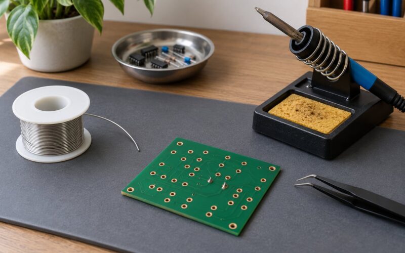
Assembly is a separate operation from fabrication, and the distinction trips up a lot of first-time buyers. Fabrication gives you a bare board. Assembly puts components on it.
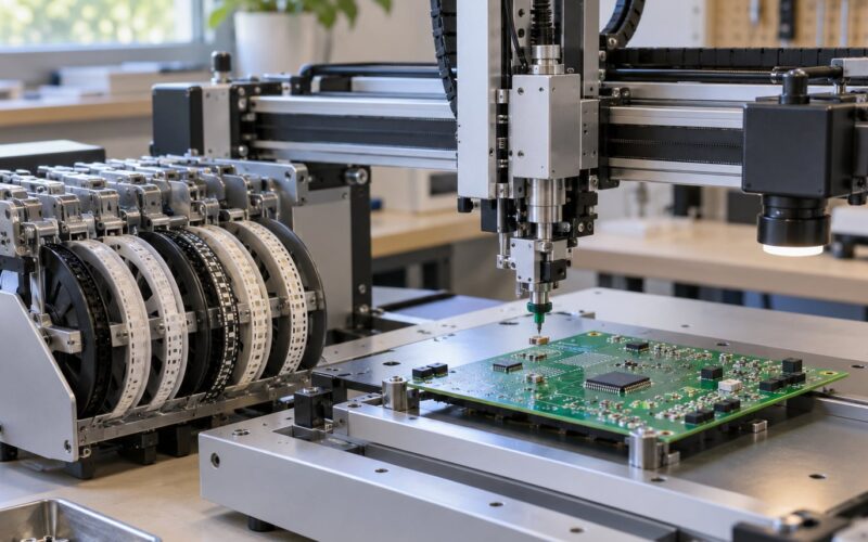
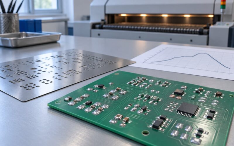
Solder paste is printed through a stencil, pick-and-place machines set components from the placement file, and the board goes through a reflow oven on a thermal profile matched to the parts. Large thermal pads on high-pin-count packages usually need selective solder or a longer soak to avoid voids, and that constraint pushes layout decisions before the design is ever released. Through-hole parts are inserted and soldered by wave or selective soldering after reflow.
Inspection moves with the process. Automated optical inspection checks polarity, placement and solder joints on visible sides. X-ray inspection looks under QFN and BGA packages, where the joints cannot be seen. Forums describe this constraint loop constantly: assembly house capability shapes the layout, and the layout changes the assembly quote.
10. Final Testing, Packaging, and Delivery
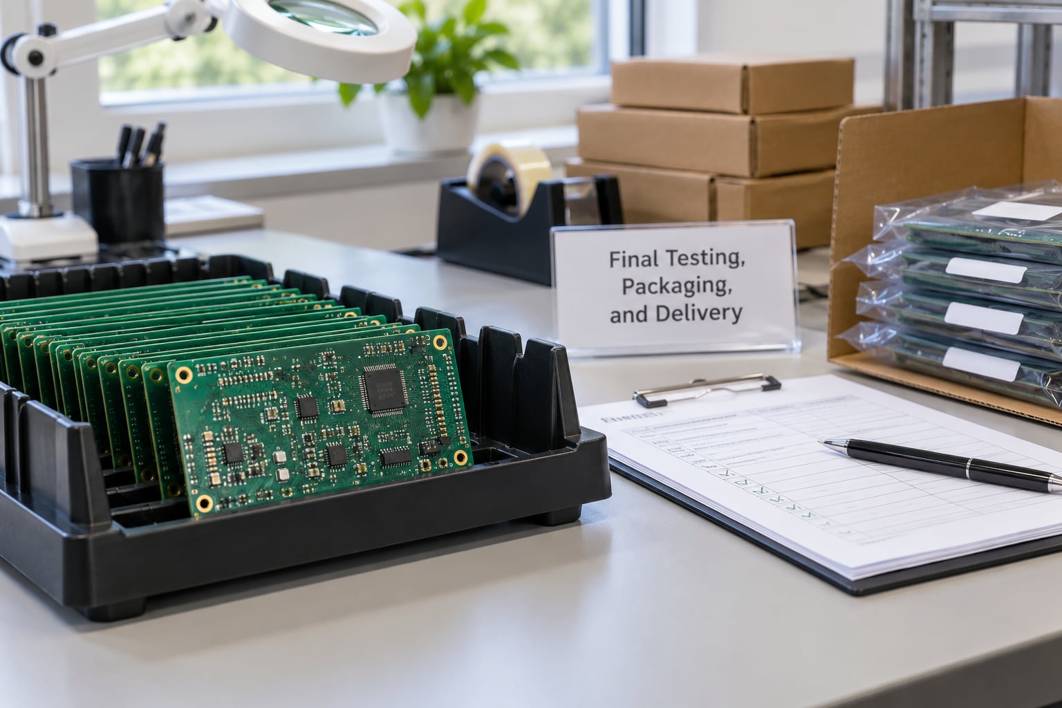
Assembled boards move to in-circuit test, which checks the component values and the populated netlist against the test program, and then to functional test, which powers the board and verifies its actual behaviour. Boards needing rework go to a rework station under a microscope before retesting. Conformal coating, potting or cleanroom wash are applied when the design calls for them, not by default.
Boards are cleaned, dried, inspected one last time and packed in anti-static trays or bags with barriers against ESD. Labels carry the part number, revision, lot code and date code. Documentation worth asking for on a bare board order includes the fabrication report, electrical test results, material and laminate certificates, impedance coupon measurements, and a statement of the IPC class the work was built to.
Ask for that documentation while the order is being placed. Reconstructing it six months later, when a field failure needs an answer, is a different and much harder job.
Common Mistakes
Most PCB defects trace back to a decision made before the factory ever touched the board. Here are the errors that repeat, and what actually fixes each one.
- Incomplete or mismatched fabrication data. The Gerber set and drill file disagree about the number of layers, or the stack-up note contradicts the artwork. Fix: freeze the release package, re-export all outputs from the same revision of the design, and run a netlist comparison before sending.
- Clearances below the fabricator’s real capability. A quoted 3 mil line and space rarely holds on a board that also needs tight registration. Fix: give yourself margin over the published minimum, and ask what the shop measures in rather than what it advertises.
- Unsupported materials or constructions. Specifying a laminate the shop does not stock, or an exotic stack-up with no process history, means a longer quote and higher risk. Fix: ask whether the material is running on the line that will build your board.
- Poor layer registration. Trace-to-trace misalignment across a stack shows up as intermittent failures that no amount of debugging finds. Fix: make sure registration and optical punch steps are in the process, and that AOI happens per layer rather than only at the end.
- Uncontrolled impedance. A target given as a single number instead of a tolerance, with no stack-up, produces a board that is nominally 50 ohm and functionally wrong at 5 GHz. Fix: state the stack-up, the impedance and the tolerance together, and request coupon measurements on every build.
- Underplated vias. Desmear and etch-back skipped or under-run leaves fibres on the hole wall and a thin barrel. Fix: specify the minimum plating thickness in the notes, and require via cross-sections or X-ray on a first article build.
- Solder mask problems. Mask creeping onto the pad, or too little mask bridging a fine-pitch gap. Fix: check mask dam geometry at review, and consider solder-mask-defined pads where you need tight annular rings.
- Incorrect drilling or missing tool compensation. Worn carbide drills give a hole that drifts from top to bottom of the panel. Fix: ask how the shop measures and compensates tool wear, and check hole tolerance against your package requirements.
- Missed inspection requirements. The order ships with no AOI per layer, no impedance coupons and no e-test records. Fix: put inspection points and deliverables into the purchase specification, not into an email conversation.
Two supplier habits help more than any checklist. Ask whether a house runs its own fabrication in-house or splits it across partners, and ask for their process capability numbers rather than their class list. Designers on r/electronics and electronics.stackexchange.com keep returning to the same point: repeatability across runs is the real question, and a house that will show you its own tolerance data has usually already answered it.
Frequently Asked Questions
What files do I need to send a PCB manufacturer?
A fabricator needs fabrication artwork (Gerber RS-274X or X2, or ODB++ / IPC-2581), an NC drill file with plated versus non-plated holes identified, an IPC-D-356 netlist, the layer stack-up with material and copper weight, and written fabrication notes covering IPC class, surface finish, tolerances and panelization. A bill of materials and pick-and-place file are only needed if you also want assembly. Send everything from one design revision so the layers cannot disagree.
Which file format is used for PCB manufacturing?
Gerber RS-274X remains the most widely accepted format, and Gerber X2 adds attributes such as pad function names. Many shops now prefer ODB++, which carries netlist, stack-up and drill data in one file, or IPC-2581, which keeps more of the design intent and supports bidirectional engineering feedback. Ask the fabricator what their CAM system imports cleanly before you export, and never assume the extension alone tells them the format.
How long does PCB fabrication take?
A bare two-layer prototype commonly runs about a week of factory time, while a multilayer build with controlled impedance and a full test program takes two to three weeks. Lamination, drilling and plating cycles dominate, and surface finish choice adds queue time because some chemistries run on fewer lines. A quick-turn expedite compresses the queue, not the process, so expect a cost premium rather than a shorter chemistry.
What is the difference between PCB fabrication and PCB assembly?
Fabrication is everything from data release through electrical test of a bare board. Assembly adds components: solder paste printing, pick-and-place, reflow, through-hole insertion, and inspection with AOI and X-ray. A buyer may order them together, but they are separate operations with separate capability requirements, and assembly house limits such as large thermal pad handling often shape the layout before fabrication ever starts.
What electrical testing is done on a bare PCB?
Bare boards are tested against the IPC-D-356 netlist for opens and shorts. Flying probe testing uses movable probes and needs no fixture, which suits prototypes. Fixture testing uses a dedicated probe bed and is faster in volume. Boards with impedance requirements also have coupon traces measured on a network analyzer, and heavy copper or multilayer builds may get X-ray inspection of via barrels in addition to electrical test.
Are PCBs easy to manufacture as a beginner?
Ordering from a fab house is straightforward; the difficulty is learning what to specify and what your design can tolerate. The practical entry point is a two-layer board with standard FR-4, HASL or ENIG, 6 mil traces and 12 mil spacing, and a clearly stated IPC class. Home etching is a different story, since bench processes struggle to hold fine geometry and repeatable plated through-holes.
How to Start a Reliable PCB Manufacturing Project
Start with the release package, not the order form. Re-export every fabrication output from a single frozen design revision, then have the fabricator run a design-for-manufacture review and send you the report before you authorize anything. Confirm the material, stack-up, copper weight and surface finish in writing, and ask for the process capability numbers they will hold themselves to on minimum trace, space, drill and plating thickness.
Then define what you will be given back: electrical test results, impedance coupon measurements, a fabrication report, material certificates, and confirmation of the IPC class the work was built to. Inspection points belong in the purchase specification, not in an email thread that nobody can find eight months later.
Once the files are validated and the acceptance criteria are agreed, the board moves into the ten-stage fabrication flow, and if you want assembly, into paste printing, placement, reflow and final test. Freeze those decisions before release, and the pcb manufacturing process step by step runs on data that actually specifies what you wanted.