A rigid-flex PCB is a single circuit board that contains both stiff sections for mounting components and thin sections that bend. Understanding the basics matters because the flex region changes how you route traces, plan bend radii, and hand the design to a fabricator. Most mistakes happen at the point where one material becomes the other.
If you are new to this, picture a wristband, a camera module folded into a housing corner, or a hard drive head assembly. Each one needs rigid electronics in some places and a controlled bend in others, and rigid-flex is how you get both in one board. That mix of support and movement is the heart of rigid flex PCB basics, and it settles your layer count before anyone draws a trace.
Table of Contents
- What Is a Rigid Flex PCB?
- How it differs from the other two board types
- Rigid Flex PCB Basics at a Glance
- How Rigid Flex PCB Construction Works
- The three zones
- What sits in the layer stack
- Common Materials and Why They Matter
- Bend Radius, Bend Direction, and Repeated Flexing
- Direction, neutral axis, and cycle life
- Rigid Flex PCB Layer Counts and Design Options
- How Vias, Traces, and Cover Layers Support Flexible Areas
- Design Rules Engineers Should Check Before Release
- How Rigid Flex PCBs Are Manufactured and Assembled
- Where Rigid Flex PCBs Are Used
- Rigid Flex PCB vs Rigid PCB vs Flex PCB
- Frequently Asked Questions
- What is the difference between rigid-flex and flexible PCBs?
- Can a rigid-flex PCB bend repeatedly during normal use?
- What is the minimum bend radius for a rigid-flex PCB?
- Can components be placed in the flexible section of a rigid-flex board?
- Are rigid-flex PCBs more expensive than standard rigid PCBs?
- Conclusion
What Is a Rigid Flex PCB?
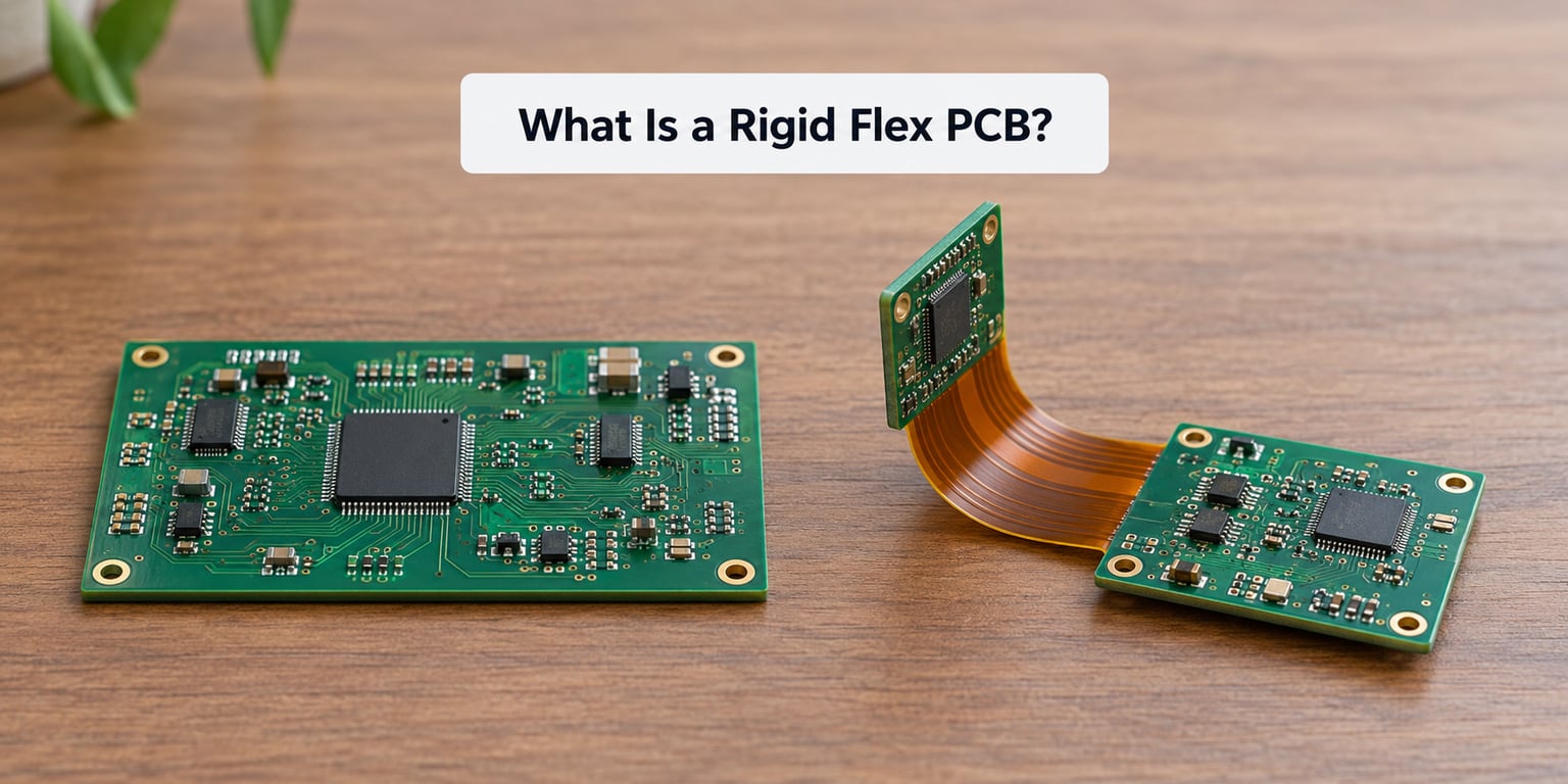
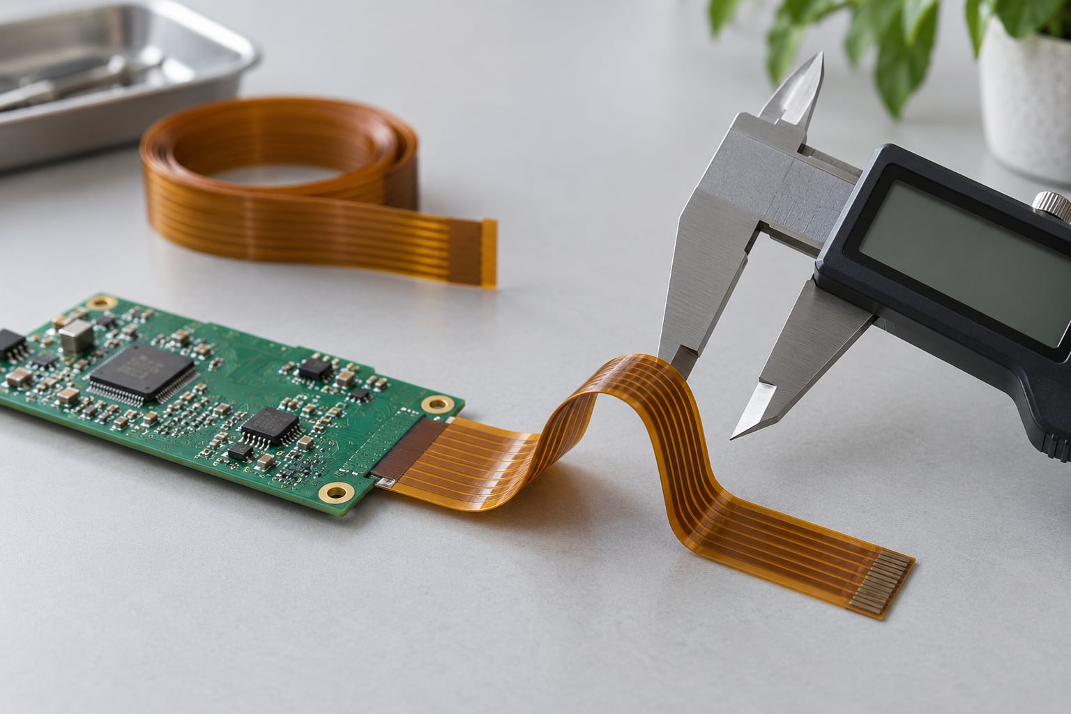
A rigid-flex PCB is one printed circuit board that combines stiff, flat sections for mounting components with thin, bendable sections that carry circuits between them. Both are joined by smooth transition zones inside a single laminate, so signals travel through the board itself instead of a wire harness or a board-to-board connector.
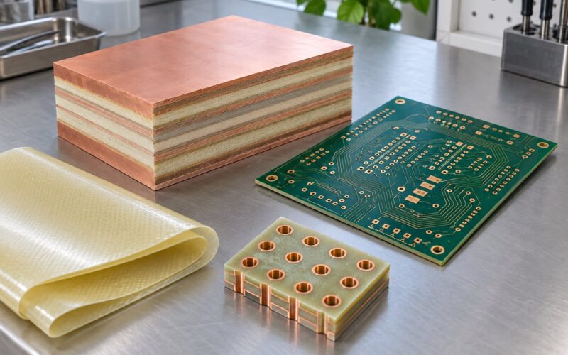
The rigid part is usually glass-reinforced laminate, the same family as a conventional FR-4 board. It handles component bodies, connectors, and heat. The flex part is a thin polyimide core with copper on one or both sides, thin enough to fold without cracking if the geometry is right.
That word “if” carries most of the engineering. A flex region is not simply a thinner rigid board. Copper, adhesive, and cover layer each behave differently as they curve, and a design that ignores that behavior fails later, often in a vibration test or after a year of use.
How it differs from the other two board types
A purely rigid PCB never moves. It is cheap, thermally stable, and easy to handle, but it cannot fold into a curved enclosure or survive repeated flexing without jointed parts.
A purely flex circuit bends nearly everywhere. It is light and routeable but hard to build, hard to assemble, and most components need stiffeners or islands to sit on properly.
Rigid-flex splits the difference. Components live on the stiff sections, the circuit passes through the bendable ones, and no connector sits at the transition. That is the whole idea behind rigid flex PCB basics, and the reason this construction shows up in wearables, medical wearables, and camera modules.
Rigid Flex PCB Basics at a Glance
This table is the quick reference version of the whole topic. Each row is expanded in its own section below.
| Aspect | What it means for your design |
|---|---|
| Board structure | One laminate containing rigid sections, flex sections, and transition zones, with no connector between them |
| Where bending happens | Only in designated flex regions, and never through a drilled via, a plated hole, or a component |
| Common materials | Polyimide flex core with rolled copper, FR-4 or similar rigid sections, adhesive bondply or no-flow prepreg, flex coverlay |
| Typical applications | Medical wearables, automotive camera and sensing modules, aerospace and defense electronics, robotics, hard drive and camera assemblies, compact consumer devices |
| Mechanical flexibility | Static bends are set once at assembly; dynamic bends cycle repeatedly and need roughly double the bend radius |
| Assembly methods | Standard SMT on the rigid regions, selective placement, plus mechanical fastening or folding of the flex region |
| Key tradeoffs | Fewer parts and less volume against higher tooling cost, more design rules, and less flexibility for last-minute layout changes |
How Rigid Flex PCB Construction Works
The mechanism that makes a rigid-flex board work is continuity. Flex layers run through the entire board, passing through the rigid sections as internal wiring, so every electrical connection between two rigid areas is made by the board itself.
The three zones
Every rigid-flex design is described as three zones. The rigid region carries components and needs no bending. The flex region is the bendable stretch that must be routed and dimensioned for a specific curve. The transition zone is where the two meet, and it is the highest-stress area on the board.
The transition gets attention because copper changes direction there. A trace running in the flex region and terminating in a via in the rigid region creates a mechanical discontinuity, which is exactly where copper cracks and delamination starts if the design does not taper it correctly.
What sits in the layer stack
A flex region is a laminate, not a sheet of copper. Typically there is a polyimide core, copper on the outer layers, an adhesive system holding them together, and a cover layer on top. The cover layer is a dielectric film that protects the copper and defines the finished surface, and it must be rated for the bend the region sees.
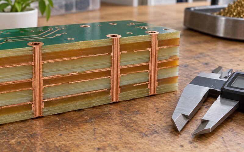
Rigid regions add the familiar FR-4 construction: glass-reinforced laminate, prepreg, copper, and finished surface treatment for solderability. A rigid-flex board is built by laminating these worlds together, often in separate presses, which is why construction styles such as bookbinder, piano hinge, and loose-leaf exist.
One practical example: a body-worn sensor patch might use a two-layer flex tail for the electrode leads, a rigid island for the amplifier, and a short dynamic bend where the tail meets the body strap. The flex layers carry the signal end to end, and the rigid island carries the parts that need a flat, stable surface.
Common Materials and Why They Matter
Material choice is where cost and durability diverge, and it is the part of rigid flex PCB basics that pays off later. The flex core is typically polyimide, chosen for tensile strength, temperature tolerance, and thinness. Rigid sections usually use FR-4 or a comparable glass-epoxy laminate because it is stiff, cheap, and easy to drill.
Copper on the flex side is often rolled rather than electrolytically deposited. Rolled copper foil is smoother and more ductile, which matters because flex copper has to survive thousands of flex cycles without work-hardening and splitting. Heavier copper carries more current but is stiffer, so it resists bending, and weight is chosen per net rather than across the whole board.
The adhesive system does more than glue. Bondply or no-flow prepreg bonds the flex layers together, and no-flow prepreg has a second job: its resin flow fills and stiffens the bend region so the board holds its shape after a fold. A prepreg that flows too freely under lamination pressure will creep into the flex area, and that is a classic source of delamination complaints.
Cover layers, plated finish, and stiffeners complete the picture. Stiffeners sit on rigid regions under heavy components, or on flex regions that must stay flat, and picking the wrong one adds thickness the mechanical team did not budget for.
Bend Radius, Bend Direction, and Repeated Flexing
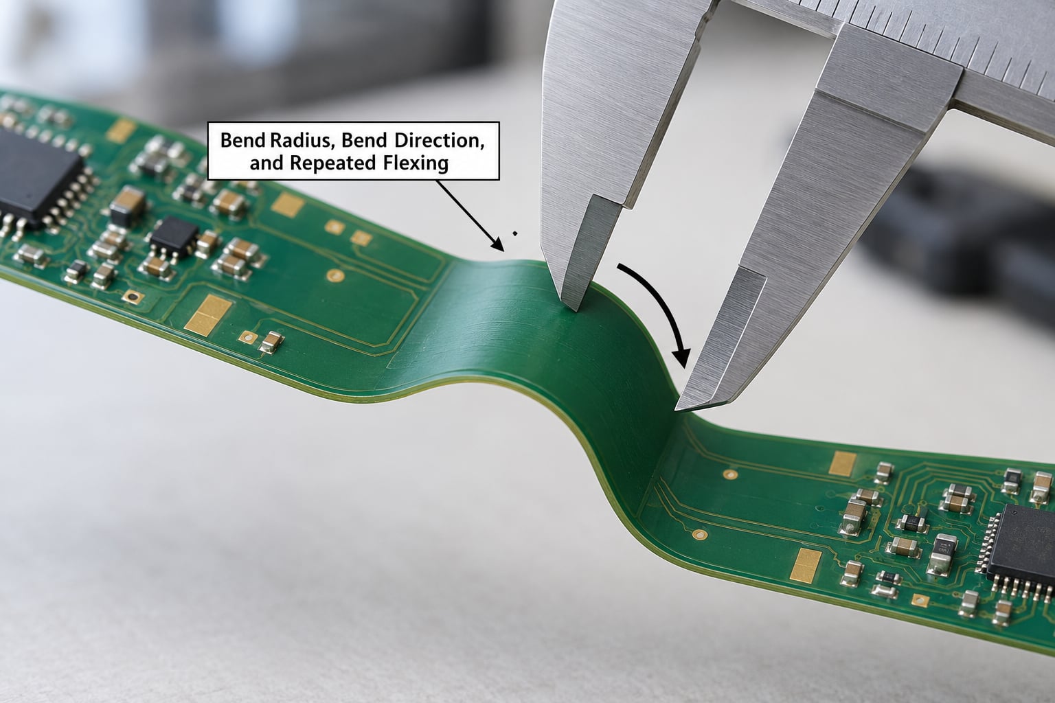
Bend radius is the single number your mechanical and electrical teams argue about most, because it ties the two together. The common rule is expressed as a multiple of flex thickness, not as an absolute dimension.
For a static bend, where the board is folded once during assembly and then stays put, the common minimum is about six times the finished flex thickness. For a dynamic bend, where the region flexes repeatedly during use, the figure rises to roughly twelve to fifteen times. Single- and double-layer flex regions tolerate the lower number; three or more layers push you toward the higher one, because each added layer thickens the stack and stiffens it.
A useful shortcut for planning: a flex region around 0.1 mm thick gives a static minimum near 0.6 mm and a dynamic minimum around 1.2 to 1.5 mm. Confirm those figures with your fabricator, since material and layer count move the real number.
Direction, neutral axis, and cycle life
Bend direction matters because a stack is strongest when it is bent with, not against, its grain and layer order. Folding the same board back and forth on the same axis in opposite directions in a short cycle is a much harsher duty than a single fold, and fabrics that are supposed to flex one way are not meant to be folded back on themselves.
The neutral axis is the layer that does not stretch when the board curves. Balanced, symmetric stacks put copper and cover layer on both sides of the core so the tension on one face matches compression on the other. Unbalanced stacks put all the copper on one side, and that is what makes flex copper crack.
Cycle life follows from radius, copper weight, and bend direction together. Tight radii, heavy copper, and reverse-axis cycling are the three things that reduce it fastest. Manufacturers spec dynamic parts in cycle counts, and if your product folds a hinge per user action rather than per test cycle, say so at design review rather than after the field returns start.
Rigid Flex PCB Layer Counts and Design Options
Layer count on a rigid-flex board is decided separately for the rigid sections and the flex sections, and the two choices interact. Flex constructions are typically one-sided, two-sided, or four-layer, while the rigid sections can run from two layers to a dozen or more, including buried and blind structures.
One-sided flex is the simplest: a single copper layer on polyimide, no vias, and the tightest possible bend radius. It suits simple signal tails, but ground returns have to share a layer, which is a problem as soon as you care about signal integrity.
Two-sided flex adds a ground or return plane, lets you run signals on one side and return current on the other, and supports plated through holes to escape to other layers. Most real designs land here because two-sided flex handles impedance control and shielding far better than one.
Four-layer flex or rigid-in-flex construction is the answer for high-density routing, split power planes, embedded shielding, or tighter spacing demands. It also raises the minimum bend radius and makes the layer count at the transition the hardest part of the design, so the extra layer should buy you something specific rather than just routing headroom.
A practical caution: every added layer adds a lamination cycle, and lamination cycles are where rigid-flex cost climbs fastest. Add a layer because a return path, a heat spreader, or a shielding plane requires it, not because the layout is crowded.
How Vias, Traces, and Cover Layers Support Flexible Areas
The flex region is a mechanical structure first and an electrical one second, and the routing rules follow from that. Traces in a flex region run with generous spacing and parallel angles, because a trace that changes direction repeatedly through a bend sees alternating tension and compression and eventually cracks.
Vias need more care. Keep drilled and plated features out of the bend entirely, and hold them back from the flex-to-rigid boundary, where a common rule is no vias within roughly 0.050 inch of the transition line. Where a trace enters the rigid region, terminate it with a teardrop rather than a hard corner, since the teardrop spreads stress across a wider area of the pad.
Neckdowns, where a trace narrows to fit between features, belong in the rigid region, not in the bend. An abrupt width change in a flex region is a stress concentration dressed up as a routing fix.
On the cover layer side, use a cover layer rated for the bend, and keep it continuous across the transition so the surface does not crack there. Stiffeners follow the same logic: they belong on rigid regions, and a flex region that needs to fold should not be stiffened in the fold.
A do and an avoid, side by side. Do taper a signal out of the flex region with a smooth, gradual path and a teardrop pad landing on a via in the rigid area. Avoid running that same signal as a sharp 90-degree dogleg through the bend, where a plated via sits a few millimeters from the curve.
Design Rules Engineers Should Check Before Release
Most rigid-flex design errors are caught at release review if someone is looking. The following checks are the ones that consistently come back from fabricators with a request for a change.
- Component placement. No parts, connectors, or test points inside a flex region or a bend. Everything mounts on a rigid section.
- Transition keep-outs. Define a transition line in the mechanical drawing, keep plated features back from it, and make sure the drawing and the layout agree about where it sits.
- Bend radius compliance. Check the finished flex thickness against your chosen multiple, then confirm the mechanical assembly can actually achieve that radius.
- Trace and via discipline. Straight parallel routing in the bend, teardrops at transitions, no neckdowns in flex, no right-angle direction changes through a curve.
- Stackup symmetry. Balance the flex layer build so the neutral axis sits in the core, and confirm copper weight choices per net rather than blanket.
- Drill and tooling limits. Some fabricators constrain drilling in flex and near transitions. Ask for their drill table before committing to a hole pattern.
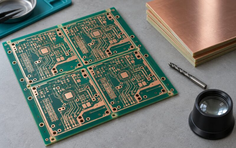
- Panelization. Rigid-flex panels break differently from rigid ones. Confirm the fabricator’s panel scheme and rails with the assembly house.
- Test access. Make sure every net can be probed from a rigid region, and agree on a flying probe or fixture strategy before layout is frozen.
- Solderability and assembly. Surface finish on rigid regions only, and a clear plan for how the flex region is handled, folded, or potted during reflow and mechanical assembly.
- Impedance and signal integrity. Keep high-speed nets out of the bend, keep return paths continuous through transitions, and flag anything that needs shielding early.
- Mechanical tolerance coordination. The board, the enclosure, the hinge, and the strain relief all have tolerances. Agree the stack thickness and bend location with the mechanical owner in writing.
One structural point deserves its own note. Many EDA tools do not treat flex zones as first-class objects, which is a genuine friction point engineers run into when starting from scratch. Some mechanical tools have no rigid-flex support at all, so teams often learn the stackup by reading a fabricator’s design guide or by asking the fabricator to review an early stackup. That review is cheap; a re-spin is not.
How Rigid Flex PCBs Are Manufactured and Assembled
Fabrication starts the way any board does and diverges in the middle. The core copper pattern is imaged by photolithography, layer by layer, and the layers are then laminated under heat and pressure into a single stack.
Rigid-flex adds a second lamination stage, because the flex region and the rigid region are pressed separately and then joined. That join is the transition, and it is where registration, resin flow, and copper-to-copper alignment have to line up within tight limits.
Drilling and plating come next. A plated through hole in a flex region is a mechanical stress riser, so the drilling and plating process here is more constrained than on a rigid board, and the flex region is often processed last or handled separately to limit handling damage.
Surface finish, cover lay, and solder mask follow, then assembly. SMT lines handle the rigid regions with standard reflow, and the flex region is supported or fixtured so its own weight does not drag on a trace during handling. Selective placement, stiffener bonding, and mechanical folding or fastening complete the build.
Inspection closes the loop: electrical test from probe points you placed on rigid regions, impedance verification, and a flex check for dynamic parts. For qualified programs, dynamic flex cycling, thermal cycling, and insulation resistance or IST-style testing are how a design earns its cycle count.
Where Rigid Flex PCBs Are Used
Applications cluster wherever three conditions overlap: a tight envelope, a moving or flexing part, and an environment that punishes loose connections.
Medical devices. Wearable monitors, patient-worn patches, hearing aids, and implantable or near-implant packaging all need thin, light boards that survive handling and body motion. Removing a wire harness removes connectors that are failure points, which is the main argument in this segment.
Aerospace and defense. Satellites, drones, and ruggedized radios put boards into vibration and temperature extremes. Rigid-flex handles shock well and mounts cleanly into tight structural pockets, and designs here are usually specified against IPC-6013 Class 2 or Class 3 with materials and finishes chosen for the temperature range.
Automotive and sensing. Camera modules, ADAS sensor units, and lidar assemblies fold a board into a housing that must survive both road vibration and a wide temperature band. A single folded board replaces a short cable and its connector pair inside a space measured in millimetres.
Wearables and consumer devices. Smartwatches, fitness trackers, foldable phones, and hearing products need a board that fits a curved body and keeps component heat away from skin. Rigid sections carry the processor and radio; flex sections wrap to the enclosure.
Industrial, robotics, and data storage. Robot joints and cable carriers need repeated flexing, which is dynamic-flex territory. Hard drive heads, camera modules, and instrumented tooling use rigid-flex to route signals into positions a rigid board simply cannot reach.
Rigid Flex PCB vs Rigid PCB vs Flex PCB
If you only remember one distinction: a flex PCB bends almost everywhere and a rigid-flex PCB bends only where you draw the bend lines. That single difference drives cost, assembly, and handling.
| Criteria | Rigid PCB | Flex PCB | Rigid-flex PCB |
|---|---|---|---|
| Structure | Solid laminate, no bendable area | Polyimide throughout, bendable across most of the surface | FR-4 and polyimide in one laminate, joined at transition zones |
| Where it bends | Nowhere | Almost anywhere | Only in designated flex regions |
| Component mounting | Everywhere, standard SMT | Restricted; often needs islands or stiffeners | On rigid regions, standard SMT |
| Assembly | Simplest and most automated | Handles delicately, often semi-manual | Rigid regions standard, flex region supported or fixtured |
| Connections between areas | Board-to-board connectors or cables | Continuous traces across the whole board | Continuous flex layers, no connector at the transition |
| Cost | Lowest, most predictable | Moderate to high per unit at volume | Highest tooling and process cost of the three |
| Durability in vibration | Good, connectors are the weak point | Good if the bend rules are respected | Very good, fewer solder joints and no harness |
| Best fit | Flat enclosures, budget-driven builds | Lightweight, fully routed flexible shapes | Tight enclosures that need component mounting and folding together |
Flex-only boards also have honest downsides worth naming. Thin flex is easy to fit into tight spaces and easy to damage, which hobbyists and engineers alike mention when comparing parts: handling, soldering, and rework all get harder on a thinner, floppier board. Component placement is restricted, repairs at the bench are less forgiving, and a flex design that folds in a product still has to be dimensioned for a real bend radius rather than assumed bendable everywhere.
Cost is the other honest one. Rigid-flex quotes are driven by layer count, the number of lamination cycles, tooling, the number of transitions, and tight tolerances. Quotes also rise when the design asks for dynamic bend specs, small bend radii, or many plated holes near transitions. A rigid board with two connectors may be cheaper than a rigid-flex board that replaces them, and for a static assembly where volume matters more than form factor, that is often the right answer.
Frequently Asked Questions
What is the difference between rigid-flex and flexible PCBs?
A flex PCB is bendable across most of its surface, so it needs islands or stiffeners wherever a component sits. A rigid-flex PCB is bendable only in defined flex regions, and the rest of the board stays stiff FR-4 that accepts standard surface-mount parts. Flex suits lightweight, fully routed shapes; rigid-flex suits products that need both folding and normal component mounting.
Can a rigid-flex PCB bend repeatedly during normal use?
Yes, when the design is built and specified for it. A dynamic flex region is dimensioned for repeated cycling, with a larger bend radius, often twelve to fifteen times the flex thickness, and copper chosen accordingly. Manufacturers rate such parts in cycle counts. The same region should not be folded once for assembly and then treated as a hinge unless the design was quoted as dynamic.
What is the minimum bend radius for a rigid-flex PCB?
It depends on flex thickness and whether the bend is static or dynamic. The common rule is about six times the finished flex thickness for a one-time static fold, and roughly twelve to fifteen times for repeated flexing, with more layers pushing the number up. So a flex region near 0.1 mm gives roughly 0.6 mm static and 1.2 to 1.5 mm dynamic. Confirm the real figure with your fabricator.
Can components be placed in the flexible section of a rigid-flex board?
Not as a rule you should follow. Components, connectors, vias, and drilled holes belong on rigid regions. If a part must sit in a flex area, the design needs a rigid island or a stiffener, which changes the local thickness and usually the bend radius around it. Placing parts directly in a bend is the most common cause of cracked copper and failed solder joints.
Are rigid-flex PCBs more expensive than standard rigid PCBs?
Generally yes, and the gap is mostly process cost rather than material cost. Layer count, extra lamination cycles, transition tooling, tighter registration tolerances, and dynamic-flex specifications all push a rigid-flex quote up. A rigid board plus a connector pair can be cheaper in low-volume, static assemblies. In high-volume builds the rigid-flex route often wins on total cost once assembly steps and harness parts disappear.
Conclusion
The mental model to keep is simple: a rigid-flex PCB is one board with two personalities, and the transition between them is the design. If the flex region is dimensioned for a real radius, routed without plated features, and kept clear of components, the board does everything a rigid board and a cable harness do together, with fewer parts to fail.
Before choosing materials or layer construction, map four things: the exact bend points and their direction, how many cycles each bend sees, where every component has to sit, and the temperature and vibration the product lives in. Those four answers fix the layer count, the material set, and whether you need a dynamic-flex construction at all. Then take the stackup to a fabricator for review before the layout is frozen, which is the cheapest hour in the whole schedule.