PCB copper weight is the nominal mass of copper on a printed circuit board, expressed in ounces per square foot (oz/ft2). Because the density of copper is fixed, 1 oz/ft2 works out to roughly 35 µm of foil thickness, so 2 oz is about 70 µm, 3 oz about 105 µm. It is a per-area measure of conductor thickness, not the weight of the finished board.
That single specification decides how much current a power path can carry before it runs hot, how much voltage you lose along the way, how difficult the board is to etch, and how tightly the geometry of your stack-up has to be controlled. Getting it wrong is expensive in both directions: too thin and a rail overheats in the field, too thick and fine-pitch routing becomes impossible.
Updated for October 2026.
Table of Contents
- What Is PCB Copper Weight?
- How Is PCB Copper Weight Measured?
- Base copper, finished copper, and plated hole wall copper
- What Does PCB Copper Weight Mean for Electrical Performance?
- How PCB copper weight changes resistance and voltage drop
- Does 2 oz copper carry twice the current of 1 oz?
- Heat spreading versus heat escape
- The 3W rule and why it is only a starting point
- Controlled impedance and fine-line capability
- Vias and barrel resistance
- How Do You Calculate Copper Weight for a PCB?
- A worked example
- Which Copper Weight Is Best for Different PCBs?
- Mixed copper-weight stack-ups
- How Does Copper Weight Affect Manufacturing and Cost?
- How to verify the copper on a delivered board
- Surface finish is not structural copper
- PCB Copper Weight vs. PCB Thickness
- How Do You Choose the Right Copper Weight?
- Common specification mistakes
- Frequently Asked Questions
- Is 1 oz PCB copper 35 microns?
- What copper weight is best for a power PCB?
- Does thicker PCB copper carry more current?
- Is 2 oz copper the same as a 70 micron finished thickness?
- How much does copper weight affect PCB price?
- Does copper weight change high-speed signal performance?
- Conclusion: Start With the Electrical Requirements
What Is PCB Copper Weight?
PCB copper weight describes the nominal mass of copper distributed over one square foot of surface area, expressed in ounces per square foot (oz/ft2). Since copper’s density does not change, that mass maps directly onto a foil thickness. 1 oz/ft2 corresponds to approximately 35 µm (about 1.4 mil) of copper.
Two clarifications matter before anything else. First, this is not the weight of the board. A 1 oz board is not heavier than a 2 oz board in the way a steel plate is heavier than an aluminium one; the difference is a few dozen grams across an entire panel, and what changes is how much current the conductors can pass. Second, oz/ft2 describes the copper foil bonded to the laminate before any pattern is etched. The finished conductor can be thicker than the foil, because electroplating adds metal to the outer layers and to the walls of every drilled hole.
| Copper weight | Thickness (µm) | Thickness (mil) | Typical use |
|---|---|---|---|
| 0.5 oz | 17.5 µm | 0.7 mil | Fine-line and HDI signal layers, very dense BGA escape routing |
| 1 oz | 35 µm | 1.4 mil | Default for signal boards; adequate for most low- and medium-current rails |
| 1.5 oz | 52.5 µm | 2.1 mil | Intermediate option where 1 oz runs warm and 2 oz breaks the line rules |
| 2 oz | 70 µm | 2.8 mil | Power conversion, motor control, LED drivers, moderate high-current paths |
| 3 oz | 105 µm | 4.1 mil | Widely accepted threshold for heavy copper; EV, battery and industrial power |
| 4 oz | 140 µm | 5.5 mil | High-current distribution, bus-like power areas, embedded copper structures |
| 6 oz | 210 µm | 8.3 mil | Motor control and contactors, power modules, on-board busbars |
| 10 oz | 350 µm | 13.8 mil | Planar transformer windings and very high-current power stages |
The 1.5 oz row matters more than its obscurity suggests. It is the step that lets a designer hold the same line and space as a 1 oz board while quietly adding roughly 50% more cross-sectional copper area, without moving all the way to 2 oz where etching tolerance starts to bite.
How Is PCB Copper Weight Measured?
The unit came from copper foil manufacturing, where sheets are weighed by the square foot. Because the density of copper is 8.9 g/cm3, the conversion to thickness is arithmetic rather than a standard: divide the mass per unit area by the density. One ounce spread across one square foot is 28.35 g over 0.0929 m2, which lands at about 34.7 µm. Designers round that to 35 µm, and fabricators quote foil in the rounded numbers.
You will also see thickness in mils (thousandths of an inch), in millimetres, and in microns. 35 µm is 0.035 mm, 0.0014 inch, 1.4 mil. The confusion starts when a single number has to describe three physically different things.
Base copper, finished copper, and plated hole wall copper
This is the most misunderstood distinction in the whole subject, and it is where spec misunderstandings are born. Three separate thicknesses exist on a finished board, and a fab drawing should name all three rather than leaving a single oz figure to be interpreted.
| Copper type | What it is | How it is made | What specifies it |
|---|---|---|---|
| Base copper (copper foil) | The foil bonded to the laminate before patterning | Rolled foil pressed into FR-4 with prepreg and core | Nominal oz/ft2 of foil, with tolerance per the foil specification |
| Finished outer-layer copper | What remains of traces and pads after plating and etching | Base foil plus electroplated copper, then pattern-etched | Finished copper thickness on the outer layers |
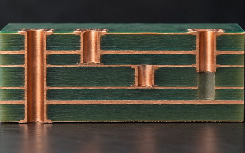
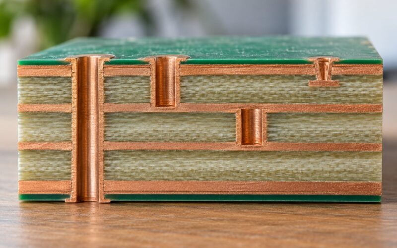
| Plated hole wall copper | The barrel lining a drilled via or PTH | Electroplating through the hole during the hole-plate cycle | Minimum plating thickness in the hole, a separate callout |
The plated hole wall is where people get caught. On a 1 oz board, surface copper finishes around 35 µm, but the barrel of a typical drilled via may only be plated to roughly 20 to 25 µm. In a power path that runs current from a top-side pad into an inner layer, the barrel — not the trace — is often the limiting resistance. If the current matters, call out hole-wall plating as its own line item.
Two standards are worth naming because they cover different ground. IPC-4562 governs copper foil thickness and its tolerances. IPC-2221 covers general board design, including plating minimums and annular ring rules. IPC-2152 is the one to quote when you size a trace for current, and it is discussed next.
What Does PCB Copper Weight Mean for Electrical Performance?
Thicker copper does three things at once: it lowers DC resistance, it raises current capacity, and it spreads heat over a larger area. All three matter, but none of them scales linearly with the oz figure, and the reason is well worth understanding.
How PCB copper weight changes resistance and voltage drop
Resistance is inversely proportional to cross-sectional area, so doubling the foil thickness at identical geometry halves the resistance. That part is exact and easy to reason about. The sheet resistance of standard copper foil works out to roughly 0.50 mΩ per square at 1 oz, 0.25 mΩ per square at 2 oz, and about 0.165 mΩ per square at 3 oz, at 20 °C.
Voltage drop is just I × R along the path, so a 1 oz trace carrying 10 A across ten squares loses about 50 mV. The same path at 2 oz loses about 25 mV. On a 12 V rail that is noise. On a 1.2 V core rail feeding a hundred amps, it is a design problem, and copper weight is often the cheapest fix available.
Temperature matters too. Copper resistance rises by roughly 0.39% per degree Celsius, so a hot power trace is measurably worse than a cold one, and this is the part that turns a voltage-drop problem into a reliability problem.
Does 2 oz copper carry twice the current of 1 oz?
No, and this is the single most repeated misconception in the space. At identical trace width, 2 oz carries roughly 1.7 times the current of 1 oz, not twice. The reason is that current capacity depends on cross-sectional area raised to the power of about three-quarters, not linearly on area, because a wider conductor sheds heat from its edges more efficiently.
IPC-2152 expresses this as I = k · ΔT0.44 · A0.75, where A is cross-sectional area in square mils, ΔT is the allowed temperature rise in °C, and k is 0.048 for outer layers and 0.024 for inner layers. Inner layers lose roughly half the capacity because they are trapped between prepreg and core with no air to help carry heat away.
| Copper weight | Layer | Trace width | Area (mil²) | Capacity at 20 °C rise | After 50% de-rating |
|---|---|---|---|---|---|
| 1 oz | Outer | 100 mil | 140 | 7.3 A | 3.6 A |
| 2 oz | Outer | 100 mil | 280 | 12.3 A | 6.1 A |
| 3 oz | Outer | 100 mil | 420 | 16.6 A | 8.3 A |
| 1 oz | Outer | 200 mil | 280 | 12.3 A | 6.1 A |
| 2 oz | Outer | 200 mil | 560 | 20.7 A | 10.3 A |
| 1 oz | Inner | 200 mil | 280 | 6.1 A | 3.1 A |
| 2 oz | Inner | 200 mil | 560 | 10.3 A | 5.2 A |
Two rows in that table are the whole argument. A 200 mil 1 oz outer trace carries the same 12.3 A as a 100 mil 2 oz trace, because they have identical cross-sectional area. Geometry and copper weight are substitutes, not partners, and the 50% de-rating column exists because continuous-duty copper conductors in free air or on a board near other heat sources are consistently optimistic in the published tables.
Ten or more variables change the answer, which is why a single rule of thumb gets quoted everywhere: ambient temperature, allowable temperature rise, duty cycle, board material and thickness, the presence of adjacent copper planes acting as a heat sink, trace length and surrounding geometry, the number and proximity of nearby hot traces, plated hole barrel size, whether the path runs on an inner or outer layer, and skin effect at higher frequencies. Generic online calculators handle a few of these and quietly assume the rest. Engineers running high-current designs regularly report that IPC-2152 tables are reliable for the trace itself but say nothing about the neighbouring heat-generating conductors or about skin effect once you are working at higher frequencies.
Heat spreading versus heat escape
Thicker copper spreads heat further before it reaches the surface, which reduces hot spots under a power device and lowers peak junction stress. It does not remove heat from the board. Heat still has to leave through the surface finish, the laminate, copper pours on the far side, or a bolted heat sink. Copper that is thick enough to serve as an on-board heat spreader usually needs somewhere to dump that energy.
The 3W rule and why it is only a starting point
The widely repeated 3W rule states that 1 mm of external trace width carries about 3 W with roughly a 30 °C temperature rise. It is a useful sanity check for outer layers in still air, and it is wrong often enough to hurt you if you treat it as a design input. A 1 mm wide 1 oz trace works out to roughly 3.9 square mils per 100 mil, and by the IPC-2152 relationship that lands near 2 A continuous at a 20 °C rise — closer to 4 A if you push the allowed rise to 30 °C. On an inner layer the same geometry gives you roughly half. Use 3W to catch a units mistake, then size the trace properly.
Controlled impedance and fine-line capability
Copper thickness feeds directly into controlled impedance because trace width and height to reference plane both set the characteristic impedance of a trace. A 1 oz stack-up that was simulated at 50 mil traces does not simply re-simulate at 2 oz with the same width; you either re-run the field solver or you deliberately design the 2 oz geometry so the finished impedance lands on target. Always re-run it.
Etching gets harder as copper thickens. Side etch grows with thickness, so a 2 oz trace etches narrower at the base and trapezoidal, and line and space requirements rise. A 1 oz board commonly supports 4 mil (0.1 mm) line and space, 2 oz usually means 6 to 8 mil (0.15 to 0.2 mm), and 3 oz pushes toward 8 to 10 mil. That is the real reason designers avoid blanket 2 oz: not the cost, but the loss of routing density on the signal layers that did not need it.
Vias and barrel resistance
A 0.3 mm finished via barrel plated to 25 µm presents far more resistance than the same current flowing through 100 mil of 2 oz trace. Stack parallel vias where current is high, specify larger finished hole sizes, or call out extra hole-wall plating on the drawing. Also mind the aspect ratio: thicker copper means more plating to balance inside each hole, and fabricators hold tighter aspect-ratio limits on heavy copper builds.
How Do You Calculate Copper Weight for a PCB?
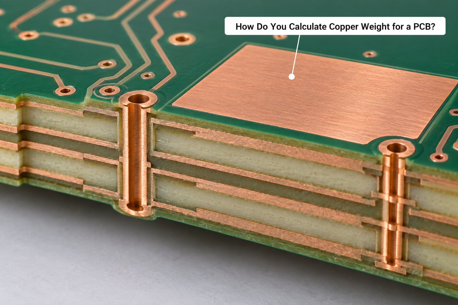
PCB copper weight explained as a number is mostly bookkeeping. You calculate the mass of copper on a board by summing the copper area on each layer, multiplying by the thickness of that layer, and multiplying by the density of copper. The formula is simple; getting defensible numbers takes a little care about which features count.
Features that count as copper: traces, pads, pour and fill areas, ground and power planes, the copper in the hole walls of plated through-holes, via-in-pad copper, and any embedded copper block or busbar. Features that do not: the areas that get etched away, the clearance around traces, the material removed to create spacing, and the copper that ends up on the scrap skeleton. On a typical signal board the skeleton scrap alone can be a third of the foil.
Also decide which thickness you are calculating with. Base copper gives the mass of the foil as supplied. Finished outer-layer copper includes plating added before etching. For a real board, calculate both and quote the finished number, because that is what carries the current.
A worked example
Take a two-layer board, 100 mm by 80 mm, with 2 oz copper on both outer layers and 30% average copper coverage on each layer after etching. The board area is 8000 mm². Copper area per layer is 8000 × 0.30 = 2400 mm², so 4800 mm² across both layers. At 70 µm, that is 0.07 mm thick, giving a volume of 4800 × 0.07 = 336 mm³ of copper. Copper weighs 0.0089 g per mm³, so the finished conductors come to 336 × 0.0089 ≈ 3.0 g.
Now add the hole plating. Forty 0.3 mm finished holes through a 1.6 mm board with 20 µm of barrel plating contribute a wall area of π × 0.3 mm × 0.020 mm ≈ 0.019 mm² per hole. Across the board length that is about 0.030 mm³ per hole, or 1.2 mm³ in total, which is roughly 0.01 g. Negligible in mass, but as noted earlier it is not negligible in a power path.
Repeat the calculation at 1 oz on the same geometry: the conductors come to about 1.5 g. So stepping a two-layer board from 1 oz to 2 oz adds roughly 1.5 g of copper per board. That is a rounding error in material terms, which is exactly why the cost of heavy copper lives in processing, not in the metal.
Which Copper Weight Is Best for Different PCBs?
One ounce remains the right default for signal integrity work, and it should stay that way unless there is a specific reason to move. Dense BGA escape routing, fine-pitch fanout, and impedance-controlled layers all get harder as copper thickens, with no electrical benefit on a trace carrying 100 mA.
Two ounces earns its place in power conversion, motor control, LED drivers, battery management, and distribution rails in the tens of amps. The jump from 1 oz to 2 oz buys meaningful resistance and temperature margin, and most fabricators run 2 oz on their standard process with no minimum-line penalty you would not accept.
Heavy copper — conventionally 3 oz and above, a threshold that is industry practice rather than a formal standard — targets EV and automotive power electronics, industrial motor and relay control, high-power computing hardware, and UPS and energy storage. Continuous high-current paths, long power runs where voltage drop adds up, and pads that will be repeatedly terminated benefit from the mechanical robustness as well as the electrical gain.
| Design factor | 1 oz | 2 oz | 3 oz and above |
|---|---|---|---|
| Nominal thickness | 35 µm (1.4 mil) | 70 µm (2.8 mil) | 105 µm (4.1 mil) and up |
| Sheet resistance | 0.50 mΩ/sq | 0.25 mΩ/sq | 0.165 mΩ/sq |
| DC resistance at same geometry | Reference | Half | About one third |
| Typical line and space | 4 mil (0.1 mm) | 6 to 8 mil | 8 to 10 mil |
| Fine-line and HDI capability | Good | Limited | Poor |
| Controlled impedance | Easiest, most common stack-ups | Workable, needs re-simulation | Rare on signal layers |
| Thermal spreading | Baseline | Meaningful improvement | Approaching on-board heat sink behaviour |
| Lamination and etch demand | Standard | Standard on most lines | More demanding, tighter process window |
Mixed copper-weight stack-ups
You do not have to pick one weight for the whole board. Mixed stack-ups put 0.5 or 1 oz on signal layers and 2 oz on power layers, which is usually the most efficient answer on a four-layer board with one signal pair and one power pair. It requires the fabricator to build a non-standard stack-up with different foil weights per layer, so confirm capability early and put the layer-by-layer weights in the drawing rather than writing “2 oz board” and hoping.
Heavy copper on outer layers only, with lighter inner layers and lightened or normal vias, is a common cost reduction that preserves most of the mechanical and thermal benefit where the heat actually is.
How Does Copper Weight Affect Manufacturing and Cost?
Thicker copper adds cost at several points, and only one of them is the metal itself.
Etching. Wider side etch on thicker foil, longer etch time in the chemistry, more base copper in the etchant, and tighter control of the final trace width. Aspect ratio and etch uniformity become process variables rather than background assumptions.
Plating and drilling. More copper has to be deposited in hole barrels to keep plating thickness proportional to surface copper, and heavy copper builds often run separate or sequential plating steps. Drilled hole quality and barrel integrity get more scrutiny on thick builds.
Lamination. More copper means more resin to fill between the layers. Poor fill shows up as resin starvation, voids, and delamination, so fabricators manage resin content and press cycles more carefully, and finished board thickness grows as the copper grows. A stack-up quoted at 1.6 mm on 1 oz may land closer to 1.67 mm on 2 oz unless the dielectric is adjusted to compensate.
Yield. Every one of those extra process variables costs yield. On a board with a large die or many BGAs, a yield point lost during etch or lamination is expensive, and copper weight is one of the levers a fabricator will ask you to reconsider if quoting gets difficult.
Balance and flatness. Heavy copper builds must stay copper-balanced across the stack-up so the board does not warp during lamination and thermal cycling, which is why thieving (dummy copper added to open areas) and bow-and-twist control matter more on a mixed-weight build.
Cost itself moves with copper weight per layer multiplied by layer count, plus the processing premium. A four-layer board going from 1 oz to 2 oz on every layer quadruples the added foil area compared with a two-layer board doing the same step, so the premium scales with layer count, board size, and how many layers carry the heavier weight. Prices change with the copper market and with each fabricator’s process, so treat the direction of the change as reliable and any specific number as something to confirm in a current quote.
How to verify the copper on a delivered board
If the copper weight is critical, verify it rather than assume it. Four methods are available, in ascending order of rigor and cost.
Coupon resistance is the cheapest: the fabricator leaves a Kelvin test coupon on the panel with a defined number of squares, and you measure it with a four-wire meter. Comparison against a known reference is straightforward.
X-ray fluorescence gives a fast non-destructive copper thickness reading on the surface, though its accuracy on very thin films and its inability to reach the inside of a hole wall both need to be understood before relying on it.
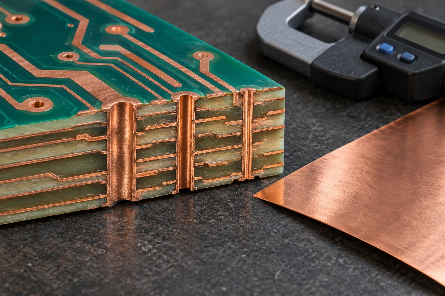
Cross-sectioning is the definitive method. Mount a sample, polish a cross-section through a trace and a via, then measure finished copper on the surface and plating thickness in the barrel under a microscope. It is destructive and slow, which is why it is usually reserved for qualification builds or suspect lots.
Dimensional and weight checks on the panel give a coarse sanity test. Buyers have raised the question publicly of whether quoted 1 oz is really 1 oz, calculating out the implied mass and asking for proof, and the honest answer is that foil carries a tolerance around its nominal weight, so material substitution and grade substitution between the quote and the delivered goods are legitimate concerns to raise in writing.
Put the requirement on the drawing and the purchase order, state whether the number is base or finished copper, name the measurement method you will accept, and ask for the certificate of conformance against that drawing.
Surface finish is not structural copper
ENIG gold thickness, immersion silver, and the solder on HASL-coated boards are measured in microns but do not count toward current-carrying copper. Two misunderstandings follow from that. First, a HASL finish adds a layer of solder that makes a trace look and measure larger than it is, so a 1 mm trace with solder on it behaves closer to a 1.5 mm trace thermally — a helpful illusion, but not one to rely on in a calculation. Second, gold flash on ENIG protects the surface and improves solderability; it does not raise ampacity.
PCB Copper Weight vs. PCB Thickness
PCB thickness is the overall finished thickness of the board. PCB copper weight is the thickness of the copper conductor layers. They are separate specifications, they are measured separately, and one does not imply the other.
A 1.6 mm board can be built on 0.5 oz foil, 1 oz foil, or 2 oz foil, because the fabricator holds total thickness by adjusting the dielectric. The common mistake runs the other way: assuming that a thicker board means thicker copper. A 2.0 mm board on 1 oz carries no more current than a 1.6 mm board on 1 oz.
Board thickness still matters on its own terms. It sets mechanical stiffness and connector insertion behaviour, it changes how heat leaves through the laminate, and longer drilled holes have a higher aspect ratio. Copper weight sets resistance, current capacity, etching, and fine-line capability. Specify them independently on the drawing and nobody has to guess which one you meant.
How Do You Choose the Right Copper Weight?
Work through these in order. Each step depends on the answer to the one before it, which is why starting with the oz figure and working backwards tends to produce a board that is either overbuilt or quietly undersized.
1. Define the current, properly. Separate continuous current, peak current, surge current, and fault current. A converter output might carry 30 A continuous and 60 A for 100 ms, and the two numbers stress the copper very differently.
2. Set a voltage-drop target. Decide how much drop across the path you can accept, including through connectors, vias, and terminals. Convert that to an allowed path resistance and work back to a sheet-resistance budget.
3. Set an allowable temperature rise. Pick the rise you are willing to live with, often 20 to 30 °C, and hold to it. This is the number that anchors every ampacity calculation that follows.
4. Size the geometry first. Using IPC-2152, size the trace width at 1 oz, then check whether that width and spacing still route in your design. In a lot of boards, they do not.
5. Check the vias, pads, and terminals. Barrel plating, via size, pad diameter, and connector rating frequently limit a power path before the trace does. A 40 A path built on two 0.3 mm vias will disappoint you.
6. Pick the copper weight. If 1 oz routes, stay at 1 oz. If it does not, step to 2 oz on the layers that need it, or widen traces into planes and keep 1 oz. Choose heavy copper only when the current, the path length, or the mechanical duty cycle genuinely requires it.
7. Confirm process capability. Check minimum line and space, aspect ratio, board thickness, and whether the fabricator will quote a mixed-weight stack-up. Ask them to confirm before you commit the layout.
8. Write it on the drawing and verify it on delivery. State finished copper per layer group, minimum hole-wall plating, and the acceptance method. Then use the coupon, cross-section, or XRF check when the first boards arrive.
Common specification mistakes
Writing “2 oz copper” with no statement of whether that is base or finished copper. Writing one weight for a mixed-weight stack-up. Leaving hole-wall plating undefined and inheriting a thin default. Specifying heavy copper on signal layers that do not need it and losing fine-line capability for nothing. Changing copper weight after layout is finished, which invalidates the routing you already did. And accepting a board without any verification step at goods-in, which is how a thin substitution reaches production.
Is my 1 oz really 1 oz? Sometimes it is less than the drawing asked for. Foil arrives with a tolerance around its nominal weight, fabricators substitute laminate and foil grades to manage availability, and surface copper loses a little to etch sidewall and to plating-thickness distribution. None of that is usually sinister, but none of it is worth discovering in a thermal chamber. Ask for the finished-copper callout, the plating callout, and a certificate of conformance against the drawing, and sample the first lot.
Frequently Asked Questions
Is 1 oz PCB copper 35 microns?
Roughly, yes. 1 oz/ft2 of copper corresponds to about 34.7 microns of foil thickness, which everyone rounds to 35 microns or 1.4 mil. The finished conductor is usually slightly thicker than the foil because electroplating adds metal to outer layers, and slightly thinner at the base of a trace because of etch undercut. Treat 35 microns as the nominal anchor, not a guaranteed measurement.
What copper weight is best for a power PCB?
Two ounces is the usual answer for power conversion, motor control, LED drivers, and rails in the tens of amps. Three ounces and above is justified for continuous high-current distribution, EV and automotive power stages, and paths where mechanical robustness at terminals matters. Start from your current, temperature-rise and voltage-drop targets rather than from a habit, because many power boards are fine on 1 oz.
Does thicker PCB copper carry more current?
Yes, but not in proportion to thickness. At identical trace width, doubling copper from 1 oz to 2 oz raises capacity by roughly 1.7 times rather than 2 times, because IPC-2152 scales with cross-sectional area raised to about the three-quarters power. Doubling trace width at 1 oz gives you the same current as keeping the narrow width at 2 oz, and inner layers carry about half what outer layers do.
Is 2 oz copper the same as a 70 micron finished thickness?
Not exactly. 2 oz describes 70 microns of base foil bonded to the laminate. Finished outer-layer copper is base foil plus electroplated copper, so it can land slightly above 70 microns. Separately, plated hole walls may only reach 20 to 25 microns even on a 2 oz board. If the number matters, specify finished copper and minimum hole-wall plating as two distinct requirements.
How much does copper weight affect PCB price?
It moves the price, but the metal is a small part of it. The real drivers are processing: wider etch allowance, longer etch time, more plating to keep barrels proportional, tighter lamination and resin-fill control, greater yield loss, and a thicker finished board. The premium scales with layer count and board size, so four layers at 2 oz costs proportionally more than two layers at 2 oz. Confirm current pricing with your fabricator.
Does copper weight change high-speed signal performance?
It changes the geometry that sets impedance, not the signal itself. Trace height and width to the reference plane determine characteristic impedance, so moving from 1 oz to 2 oz changes impedance unless you re-run the field solver for the new stack-up. Thicker copper also makes fine lines harder to etch, which can hurt BGA escape routing. On loss and crosstalk, geometry and dielectric dominate rather than copper weight.
Conclusion: Start With the Electrical Requirements
PCB copper weight is the thickness of the conductor, quoted as mass per square foot, and it sets resistance, current capacity, temperature rise, etch difficulty, impedance geometry and cost. Thicker copper roughly halves resistance at the same geometry, but it does not double current capacity, and geometry is often the cheaper lever.
Work in this order: current, then voltage-drop target, then allowable temperature rise, then trace geometry, then vias and terminals, and only then the copper weight. Write base copper, finished copper and hole-wall plating as three separate lines on the drawing, and verify the result on the first delivered lot.