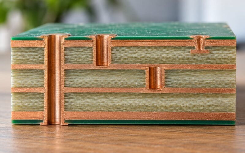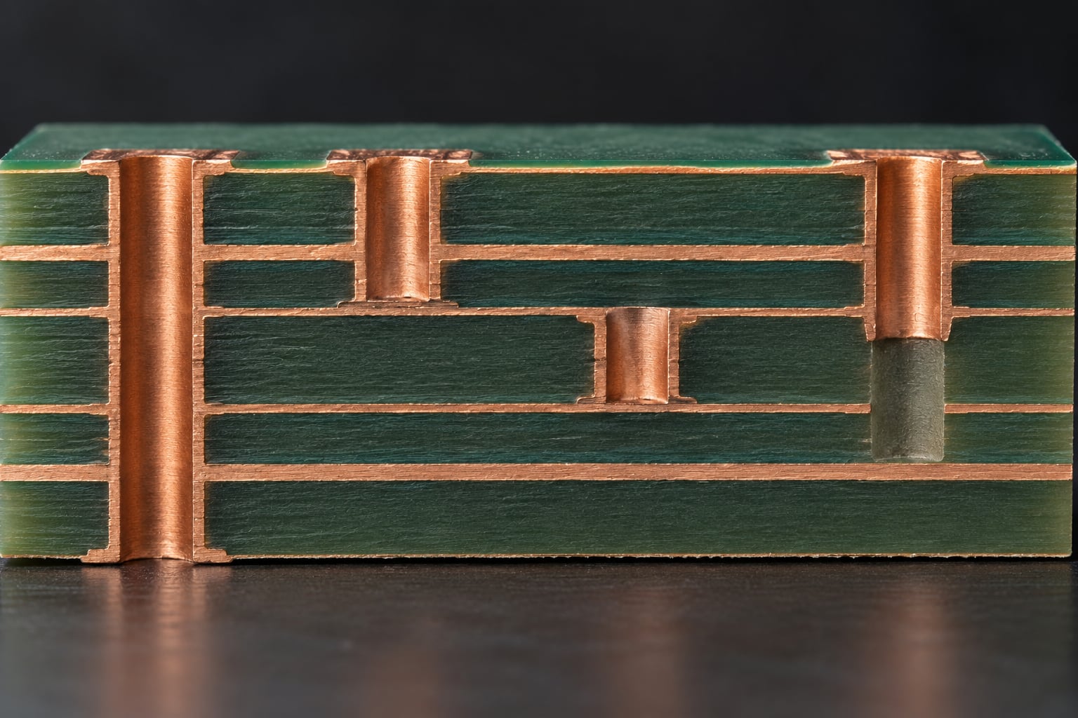
A plated through hole (PTH) is a copper-plated hole that runs the full thickness of a printed circuit board, connecting every conductive layer it passes through. A blind via is also copper-plated, but it starts at one layer and stops at an internal layer instead of passing through the board. That single difference decides routing density, cost, inspection method, and signal behaviour.
The confusion around the term is worth clearing up first, because most of the top-ranking pages on this topic blur it. A through hole is usually a hole made for a component lead. A plated through hole can mean either that component hole, when it has a copper barrel, or a through-hole via used purely as an interconnect between layers. When engineers say “PTH” in a plated through hole vs blind via discussion, they almost always mean the via.
So which should you use? A plated through hole wins on cost, simplicity, mechanical strength and inspectability. A blind via wins when you need routing density on a thick, high-layer-count board, a short electrical path between an outer layer and its neighbouring inner layer, or a stub-free transition on a high-speed signal. Everything else in this guide is detail hanging off that one-line verdict.
Table of Contents
- Plated Through Hole vs Blind Via at a Glance
- Plated Through Hole: Full-Board Connections
- Two different things wear the PTH label
- Blind Via: Controlled Interlayer Connections
- Blind is not the same as buried
- The four via types at a glance
- How Plated Through Hole and Blind Via Fabrication Differ
- Through-hole process
- Blind via process
- Why depth control makes blind vias harder
- Aspect ratio and spacing limits
- Electrical Performance and Signal Integrity
- Working out the stub
- It also depends on the return path
- Plating thickness changes the resistance
- Mechanical Strength, Thermal Performance, and Assembly
- Solderability and solder wicking
- Assembly and repair
- Cost, Density, and Design Tradeoffs
- Where the premium actually goes
- When not to use blind vias
- Which Should You Choose?
- Frequently Asked Questions
- What is the main difference between a plated through hole and a blind via?
- Are blind vias stronger than plated through holes?
- Can I use a blind via for high-speed signals?
- Is a plated through hole better for a prototype PCB?
- When should a PCB designer use a buried via instead?
- How do plated through holes and blind vias affect PCB cost?
Plated Through Hole vs Blind Via at a Glance
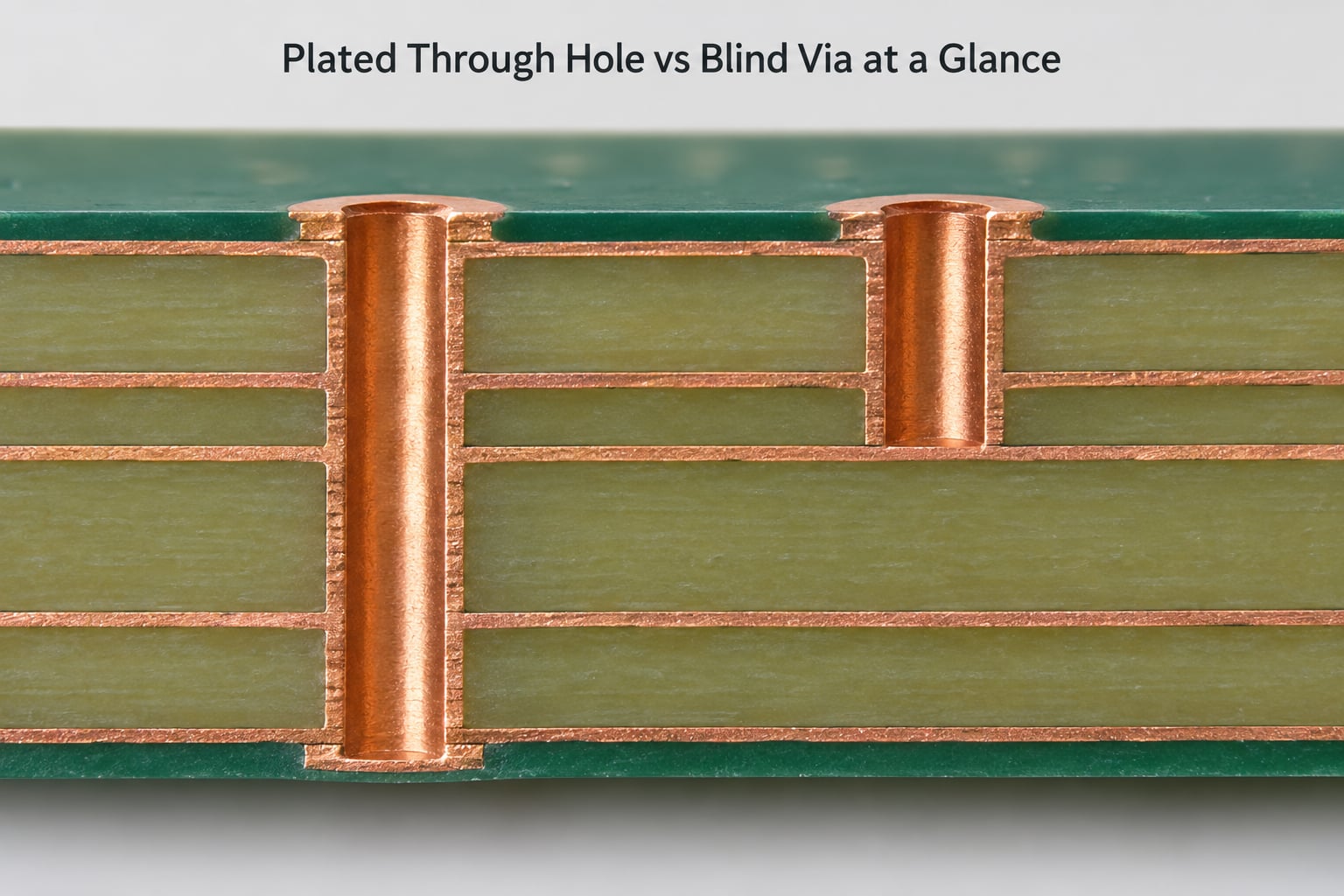
| Criterion | Plated through hole (PTH) via | Blind via |
|---|---|---|
| Connection span | Top outer layer to bottom outer layer, touching every layer it crosses | One outer layer down to one internal layer, then stops |
| Board thickness consumed | Full finished thickness, plus drill allowance for breakout | Only the distance between the two layers it joins |
| How it is made | Mechanical drill through the whole stack in one pass, then plated | Controlled depth drilling, laser ablation, or built layer by layer in sequential lamination, then plated and usually filled |
| Typical aspect ratio | Comfortable up to roughly 10:1 on a standard mechanical drill | Targeted at 1:1, accepted up to 1.5:1 for laser blind vias; mechanical blind vias held under about 8:1 |
| Fabrication complexity | Single-pass, drilled with the rest of the board | Extra process steps, tighter depth tolerance, extra lamination cycles |
| Relative cost | Baseline | Typically a 20 to 30 percent premium for complex via structures |
| Mechanical strength | Strong; a good anchor for a component pin, connector or press-fit | Weaker in the axis of the hole; not suitable for mechanical loading |
| Routing density | Consumes a full-diameter keepout on both outer layers | Leaves outer layers almost entirely free for components and fine routing |
| Inspection | Visible on the outer surfaces and on cross-sections | Not visible; needs X-ray or microsectioning to verify |
| Signal stub | Creates an unterminated stub on the unused span below the signal layer | No stub on the far side, because the barrel stops where it is needed |
| Typical use | General routing, power distribution, prototypes, through-hole parts and connectors | Fine-pitch BGA fanout, HDI boards, compact products, high-speed links |
One caveat on every row above: the numbers are fabricator-dependent. A prototype shop and a volume HDI line will quote different aspect-ratio limits, minimum diameters and lamination capability, so confirm the rules in your fab’s capability sheet before you release Gerbers.
Plated Through Hole: Full-Board Connections
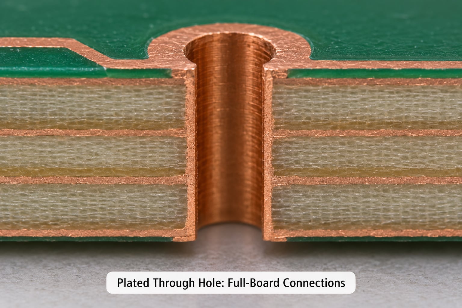
A plated through hole is a hole that has been drilled clean through the finished board and then lined with copper by the electroless and electroplating process. The barrel of copper on the hole wall is the electrical connection. It touches every copper layer the hole passes, which is why a single PTH can carry a signal, a ground reference, or power between any two layers without a trace running across the board.
That “touches every layer” property is both its strength and its problem. Strength comes first: a plated barrel is the most reliable mechanical anchor available on a bare PCB. Component leads, connectors, and press-fit hardware all depend on it, and a board that flexes in service depends on that barrel staying bonded to the barrel wall. A finished 2 oz copper barrel on a 13 mil finished hole survives insertion force, soldering heat, and repeated thermal cycling far better than a laser-drilled microvia does.
Two different things wear the PTH label
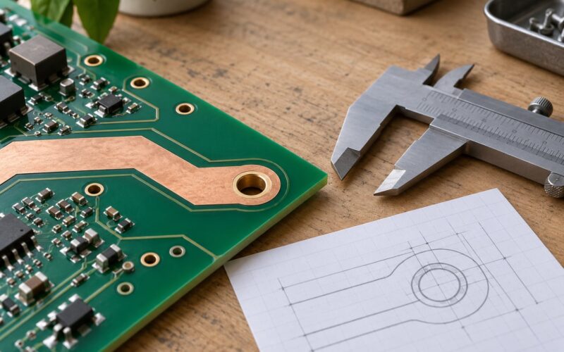
A plated through hole used to mount a part is a mechanical and electrical interface. A plated through hole used as a via is purely an interconnect, often with no component anywhere near it. Most beginners mix these up, and so does a lot of published material. When a fab talks about PTH tooling and plating thickness, it means both, because they are made in the same pass.
Designers reach for a PTH via when routing is not tight, when the board is two or four layers, or when the connection has to carry real current. Copper cross-section on a 13 mil plated hole is substantial, which is why through-hole vias still handle the main power paths on many mixed-signal boards even when the signals around them use microvias.
There is also a prototyping argument that gets overlooked. A two-layer or four-layer board with only through-hole vias needs one lamination cycle and one drill pass. It is the fastest thing a fab can build, and the cheapest thing they can quote when the design is otherwise ordinary.
Blind Via: Controlled Interlayer Connections
A blind via is a copper-plated hole that begins at an outer layer and terminates at an internal layer. It stops blind, which is the origin of the term. The microvia is simply the smallest practical version of the same thing, usually laser-drilled to a diameter of 3 mils (0.076 mm) or 4 mils, used to escape from a fine-pitch BGA pad into the next layer.
What the blind via buys is surface area. A through-hole via occupies its full diameter as a keepout on both outer layers, whether or not you route anything through it. A blind via connecting layer 1 to layer 3 still eats the layer 1 pad, but the bottom side of the board stays clear. On a phone-sized HDI board where every square millimetre of both outer layers is spoken for, that difference is what makes a fine-pitch device routable at all.
Blind is not the same as buried
This is the single most common design error I see in blind via definitions. A blind via runs from an outer layer to an inner layer. A buried via runs from one inner layer to another, and its hole is never open to the surface. Both are plated, both are invisible from outside, but they are built and inspected differently.
Back-drilled vias are a third thing again, and it is a post-lamination operation rather than a construction type. More on that below, because it is the practical middle path most designers miss.
The four via types at a glance
| Via type | What it connects | How it is produced | Stub | Where it earns its cost |
|---|---|---|---|---|
| PTH via | Outer layer to outer layer, touching all inner layers on the way | Mechanical drill through the full stack, plated | Yes, on the unused span | General routing, power, prototypes, through-hole parts |
| Blind via | Outer layer to one inner layer | Controlled depth drill, laser, or sequential lamination, plated and filled | No | BGA fanout, high-speed transitions, dense routing |
| Buried via | One inner layer to another | Sequential lamination or controlled depth drill from either side | Depends on construction | Layer-to-layer interconnect in thick multilayer builds |
| Back-drilled via | Outer layer to an internal layer, made from a PTH | Plated through, then re-drilled to depth to remove the unwanted copper barrel | No, if drilled deep enough | Stub removal on an existing through-via design |
Note that back drilling solves a specific problem rather than being a cheaper blind via. You pay for a full through via, and then you pay again to remove the part you did not want. It is worth it when a small number of high-speed transitions dominate a design and you cannot justify re-stacking the whole board.
How Plated Through Hole and Blind Via Fabrication Differ
The drilling is the easy part. Everything after it is where blind vias get expensive.
Through-hole process
For a conventional board, the stack is laminated once, drilled through in a single pass with a mechanical drill on an NC drill machine, and then desmearmed and plated. The holes are all plated in the same electroless copper seed step followed by electroplating. Imaging, etching, solder mask and surface finish follow as usual.
Drill depth is not really a variable. The drill goes through; what varies is how much of the drill tip breaks out on the exit side, and every fab has a breakout allowance in its capability sheet.
Blind via process
Blind vias come from one of four routes, and they differ mainly in cost and in which layers they can reach.
- Controlled depth drilling. A CNC machine drills to a programmed Z depth rather than through. It is the least expensive method and works well on thicker mechanical blind vias, but depth tolerance is limited and it cannot reach past the middle of the board.
- Laser drilling. CO2 or excimer ablation removes resin and copper without mechanical contact, giving small diameters and accurate depth. This is the standard route for microvias and laser blind vias. Because the copper must be plated rather than relying on the laser to form a conductive wall, the aspect ratio target is 1:1, with some fabricators accepting up to 1.5:1.
- Photo-defined vias. A dry film or liquid photoresist is imaged and developed on the prepreg, ablated by excimer laser, and the resist stripped. Very clean geometry on one layer pair at a time.
- Sequential lamination. The board is built partway, drilled and plated, capped with prepreg, laminated again, and the cycle repeats. This is the only clean way to build a buried via or a blind via that skips layers, and it is the most expensive because every cycle adds handling, process steps and yield loss on thin material.
Most HDI boards combine two of these. A build-up structure often uses laser microvias for layer 1 to 2 fanout, then sequential lamination to add the rest of the stack.
Why depth control makes blind vias harder
A through hole either worked or it did not, and you can look at both ends. A blind via has one opening and a blind floor, and its quality depends on a plating deposit inside a cavity you cannot see. Fill and via-plug materials are normally added so no air remains trapped when the board goes through reflow at around 260 C. A partially filled blind via with a void can look perfect on the outside and still fail later.
Registration matters too. A laser that over-drills by even a little can nick the annular ring or the pad on the layer below, which is a plating defect waiting to happen. Most fabs keep the drill depth off the target layer by a defined margin for exactly this reason, and that margin has to be inside your design rules.
Aspect ratio and spacing limits
| Via class | Typical aspect ratio target | Minimum diameter | Where it sits |
|---|---|---|---|
| Mechanical through via | Up to roughly 10:1 on a standard build | 8 to 10 mil finished | Full board |
| Mechanical blind or buried via | Held under about 8:1 | 8 to 10 mil finished | Outer to inner, or inner to inner |
| Laser blind via | 1:1 target, up to 1.5:1 where the fab allows | 4 mil typical | One layer pair |
| Laser microvia | 1:1 | 3 mil (0.076 mm) minimum | BGA fanout, build-up |
Aspect ratio here means hole depth divided by finished hole diameter. It matters because the plating bath has to wet the full wall; the deeper and narrower the hole, the harder it is to plate uniformly and the more likely you get a void or a thin barrel.
Spacing rules follow the same logic. Minimum via-to-via spacing of 8 mils and via-to-pad clearance of 6 mils are common design targets for HDI work, and both exist because fabricators need copper between adjacent features to plate and to etch cleanly. Exceed them and the fab will either shrink your features or ask you to change the design.
Electrical Performance and Signal Integrity
Via type changes signal integrity through one mechanism: the stub. When a signal transitions from an outer layer to an inner layer through a plated through hole, the barrel continues below the destination layer with copper on it. That continuation is an unterminated branch, and it behaves like a small antenna.
The branch has inductance, and with inductance you get a resonant peak somewhere near a frequency determined by its length and its termination. It also adds capacitance to the transition. On a slow signal neither matters. As edge rate climbs, both come forward fast, which is why blind vias start appearing in designs as soon as edges get aggressive.
Working out the stub
Rough rule of thumb for FR-4: a signal travels about 150 millimetres per nanosecond, which is roughly 6.7 ps per millimetre of copper, or about 170 ps per inch. Take a 1.6 mm board where a signal drops from layer 1 to layer 3 through a through via, with layer 3 sitting 1.4 mm above the bottom copper. The stub below the signal layer is that entire 1.4 mm of barrel, so you carry about 9 ps of extra one-way delay, and close to 19 ps once the signal reflects off the open end and comes back. That round trip is what the receiver actually sees.
Now compare that against the edge. If the rise time is a small fraction of the round-trip delay, the stub starts driving reflections hard enough to close your eye diagram. Designers often quote roughly 4.8 Gb/s as the point where via stubs stop being theoretical, and on a thick board where a signal drops several layers that problem can show up well below it. Above that range, a blind via that stops on the target layer has no stub at all, which is the whole argument.
It also depends on the return path
A layer transition has to be accompanied by a return path. When a signal drops through a via, the return current has to come back on a plane. If the next layer down is a solid plane with no void under the via, the reference is continuous. If you have split planes or a poorly placed anti-pad, the return current is forced to detour around the gap, and that detour is often a bigger integrity problem than the via stub.
So the honest ranking is not “blind vias are faster”. It is that for a given stackup, impedance control and return-path design, a blind via removes one failure mode a through via carries. Get the reference plane right first, then choose the via type.
Plating thickness changes the resistance
A barrel’s DC resistance scales inversely with cross-section. A 13 mil hole with 1 mil plating carries more current with less heating than a 4 mil microvia with 0.5 mil plating by a wide margin. For power vias, through-hole barrels remain the practical answer; for signal escapes near a fine-pitch device, nobody is putting a through hole there.
Mechanical Strength, Thermal Performance, and Assembly
Strength is the clearest dividing line. A plated through hole is a structural feature. The barrel runs the full board thickness, so a connector pin or a mounting hole supported by a PTH will hold insertion force and vibration load. Blind vias are not designed for that at all; the barrel ends at an internal layer and the copper at that floor is thin. Load the board through a blind via and you are relying on a small annular ring and a solder fillet.
Thermal conduction follows the same pattern. A through-hole barrel is a copper column the height of the board, which is why heavy-current parts are still mounted through-hole rather than on a via array. A blind via conducts heat between two layers just as well as any other copper, but it cannot move heat from one face of the board to the other.
Solderability and solder wicking
Here the through hole has a known downside. During reflow, a through hole can wick solder down the barrel, pulling solder out of the joint and leaving a weak connection. The usual fixes are a larger hole-to-pad ratio or deliberate pad open design. Blind and microvias carry the same wicking behaviour inside their fill, which is why filled and capped vias, using conductive ink, silver fill, or LPI solder-mask plug, are specified on high-density boards: to keep solder out of the cavity and keep air out during reflow.
Assembly and repair
Through-hole parts are still easier to hand-assemble, easier to inspect under a microscope, and easier to repair with an iron. A blind via needs none of that, because nothing is inserted into it. What it does need is verification before you populate the board.
- Electrical test at the netlist level, which catches open and short barrels but not a thin one.
- X-ray inspection, the standard method for blind and microvias, since the barrel floor and fill cannot be seen otherwise.
- Microsectioning on a sample, usually a cross-section cut and polished to inspect plating thickness and voids at the floor.
- Impedance or TDR measurement where controlled impedance traces are in the design.
- Thermal cycling and surface insulation resistance testing for automotive-grade work, where the -40 C to 85 C range is common.
Full electrical testing methods for finished boards are a bigger topic than this one. For via integrity specifically, X-ray plus microsection on a sample is the combination that actually tells you something.
Cost, Density, and Design Tradeoffs
The honest answer on cost is a range, not a number. Manufacturer guidance for boards with complex via structures clusters around a 20 to 30 percent premium, and broader industry figures for HDI builds with blind and microvias sit in a 10 to 30 percent band. Treat that as a ballpark you negotiate against, not a quote.
Where the premium actually goes
- Extra lamination cycles. Sequential lamination builds the board in pieces. Each cycle is a separate press run, a separate imaging step and another chance to damage thin material. ProtoExpress and others advise keeping lamination cycles to roughly two or three for cost efficiency.
- Thin-laminate handling yield. Every cycle means handling prepreg that is far more fragile than a finished board. Scrap is more likely, and on a prototype run that risk lands entirely on you.
- Additional process steps. Laser or controlled-depth drilling, a separate plating and filling operation, then capping or plugging.
- Inspection. X-ray and microsectioning are real per-board or per-lot costs that a through-via build does not incur.
What you get for that money is density. A blind via connecting layer 1 to layer 3 uses a fraction of the routing resource of a through via, which is why HDI boards routinely replace what would have been eight layers with six layers plus build-up microvias. That substitution is often where the money comes back: fewer prepreg sheets, fewer lamination cycles, thinner board, lower overall cost. The via premium is real, and it is frequently offset rather than additive.
When not to use blind vias
This is the section most competitor articles skip, and it is the one that saves you money.
- Two or four layers with normal routing density. A through via costs nothing extra and does everything you need.
- Low-cost, high-volume work where every process step is multiplied by thousands of boards. The premium per unit is small; the premium as a percentage of margin is not.
- Prototypes with loose timing. A sequential-lamination board can be scrapped in a way a single-cycle board will not.
- Any design where you have not confirmed the fabricator actually builds the via structure you drew. Capability varies more than most design rules admit.
There is a middle path too. If you need stub-free behaviour on a handful of critical transitions but not a full HDI stack, ask your fabricator about back-drilling the through vias on those nets. It costs a drilling step, it needs a depth target in your stackup, and it converts the PTH into something that behaves like a blind via on that layer pair.
Which Should You Choose?
Work down this list and stop at the first answer that applies.
- Does anything get mounted, pressed into, or pulled on through the board? Use a plated through hole. Connectors, switches, mounting hardware and through-hole parts all belong there.
- Is your board two or four layers with ordinary routing? Use through vias. Nothing else is justified.
- Are you carrying high current across layers? Use through vias, with plating thickness specified rather than assumed.
- Do you have a fine-pitch BGA, or are you out of routing space on the outer layers? You need microvias. This is where blind vias stop being optional.
- Do you have a small number of high-speed transitions where a stub matters? Use blind vias for those nets, or back-drill the through vias if the layer count does not justify a build-up.
- Are you building HDI with layer skip routing? You are in sequential lamination territory. Confirm your fabricator’s aspect ratio and microvia limits against your stackup before release.
- Still unsure? Send the stackup to the fab and ask for their capability sheet, then design inside it. Capability confirmation is worth more than any rule of thumb in this article.
The through-holes-versus-blind-via question resolves quickly once you separate mechanical needs from routing needs. Mechanical needs go to the plated through hole, always. Routing and signal needs decide the rest, and they are the only reasons to spend more.
Frequently Asked Questions
What is the main difference between a plated through hole and a blind via?
A plated through hole is drilled and plated through the entire board, so its copper barrel connects every conductive layer it passes. A blind via is plated but stops at an internal layer, starting at an outer layer and never reaching the other side. That is the whole structural difference: full span versus partial span.
Are blind vias stronger than plated through holes?
No. A plated through hole barrel runs the full board thickness and is the strongest mechanical feature on a bare PCB. A blind via barrel ends at an internal layer with thin copper at the floor, so it is not designed to carry insertion force, vibration load or mounting hardware. Use blind vias for routing, not for structure.
Can I use a blind via for high-speed signals?
Yes, and it is often the right choice above roughly 4.8 Gb/s. A blind via ends on the signal layer, so it leaves no unterminated stub to radiate or ring, and it adds less parasitic capacitance than a through via. The return path on the destination layer still matters more than the via type itself.
Is a plated through hole better for a prototype PCB?
Usually, yes. A through-via-only board needs one lamination cycle and one drill pass, which is the fastest and cheapest process a fabricator offers, with the lowest scrap risk on small runs. Blind vias add build-up steps and handling of thin material, and that risk lands on a small prototype order.
When should a PCB designer use a buried via instead?
When the connection is between two internal layers and neither endpoint is on the surface. A buried via is never open to the outside, so it is built by sequential lamination or drilled from one side to depth. It saves outer layer area in the same way a blind via does, but it adds a lamination cycle and cannot be visually inspected.
How do plated through holes and blind vias affect PCB cost?
Through vias are the baseline. Boards with complex blind or buried via structures typically run a 20 to 30 percent premium, and broader HDI figures sit around 10 to 30 percent. The premium comes from extra lamination cycles, additional process steps, thin-laminate handling yield loss and X-ray or microsection inspection.
Start by deciding whether the hole has a mechanical job. If a connector, a mounting point or a through-hole part needs support, that is a plated through hole and no amount of routing pressure changes it. Everything else on the board is a routing decision: use through vias while they still fit, and move to blind or microvias at the first layer that genuinely runs out of room or starts fighting you on signal integrity.
Before you release the design, send your stackup to the fabricator and check their aspect ratio limits, minimum microvia diameter, spacing rules and lamination count against what you drew. That single email catches more real problems than any guideline in this guide.