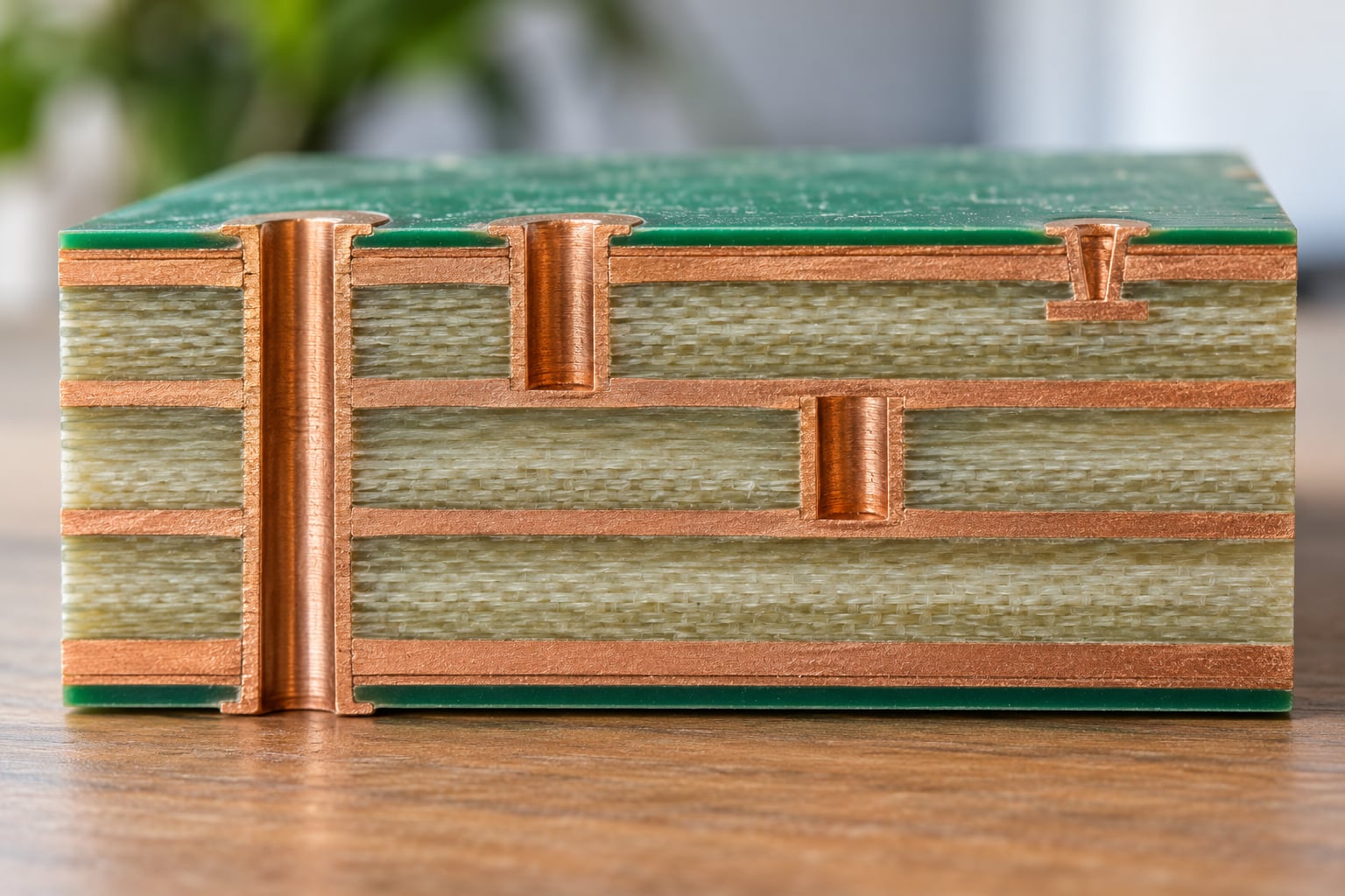
A PCB via is a hole drilled into a printed circuit board and plated with copper so it forms a conductive barrel joining two or more copper layers, which is the only way a signal or power can move in the Z direction. PCB via types explained simply: the type is decided by which layers the barrel starts and ends on, and by how the hole is drilled.
There are four primary constructions to design around — through, blind, buried, and microvia — plus variants built from them, such as stacked microvias, via-in-pad, back-drilled, filled and capped, and tented vias. Real boards mix several of these on the same design, and the choice changes routing density, signal behaviour, board thickness capability, cost and lead time in one move.
That last part is why via selection belongs at the start of a stack-up conversation rather than the end. Get the via type wrong and the board may not be manufacturable by the shop you chose, and you find out after the design is frozen.
Table of Contents
- PCB Via Types Explained: What Is a Via?
- The Main PCB Via Types at a Glance
- PCB via types explained side by side
- Through Vias: The Standard Connection Between PCB Layers
- Blind Vias: Connecting Selected Inner Layers
- Buried Vias: Internal Connections Without Outer Access
- Microvias: Small Vias for Dense PCB Designs
- What via-in-pad changes
- Mechanical Vias: When the Hole Serves More Than an Electrical Purpose
- How PCB Via Types Affect Electrical Performance
- Resistance and current capacity
- Stubs and signal integrity
- How to Choose the Right PCB Via Type
- Fabricator capability checklist
- Manufacturing and Design Considerations for PCB Vias
- Design rules worth writing into your library
- Glossary
- Common Misconceptions About PCB Via Types
- Frequently Asked Questions
- What are the types of vias?
- Are blind and buried vias the same thing?
- What is a microvia and how is it different from a through via?
- What is via-in-pad and why does it cause solder problems?
- What is a via stub and how do you remove it?
- Why are blind and buried vias more expensive than through vias?
- Conclusion: Start With the Simplest Via That Meets the Design
PCB Via Types Explained: What Is a Via?
A via has three parts. The pad is the copper landing where a trace meets the hole, the barrel is the electroplated copper wall inside the hole, and the antipad is the clearance void that keeps the barrel isolated from any plane layer it passes through.
Drilling alone makes nothing electrical. The plating is what turns a hole into a connection, which is why barrel plating quality, not drill diameter, is the usual reason a via ends up open.
Four things decide which via type you get: the start layer, the end layer, the drill method (mechanical versus laser), and what the via has to carry (signal, power, heat, or nothing at all). Once those are set, the type follows.
The Main PCB Via Types at a Glance
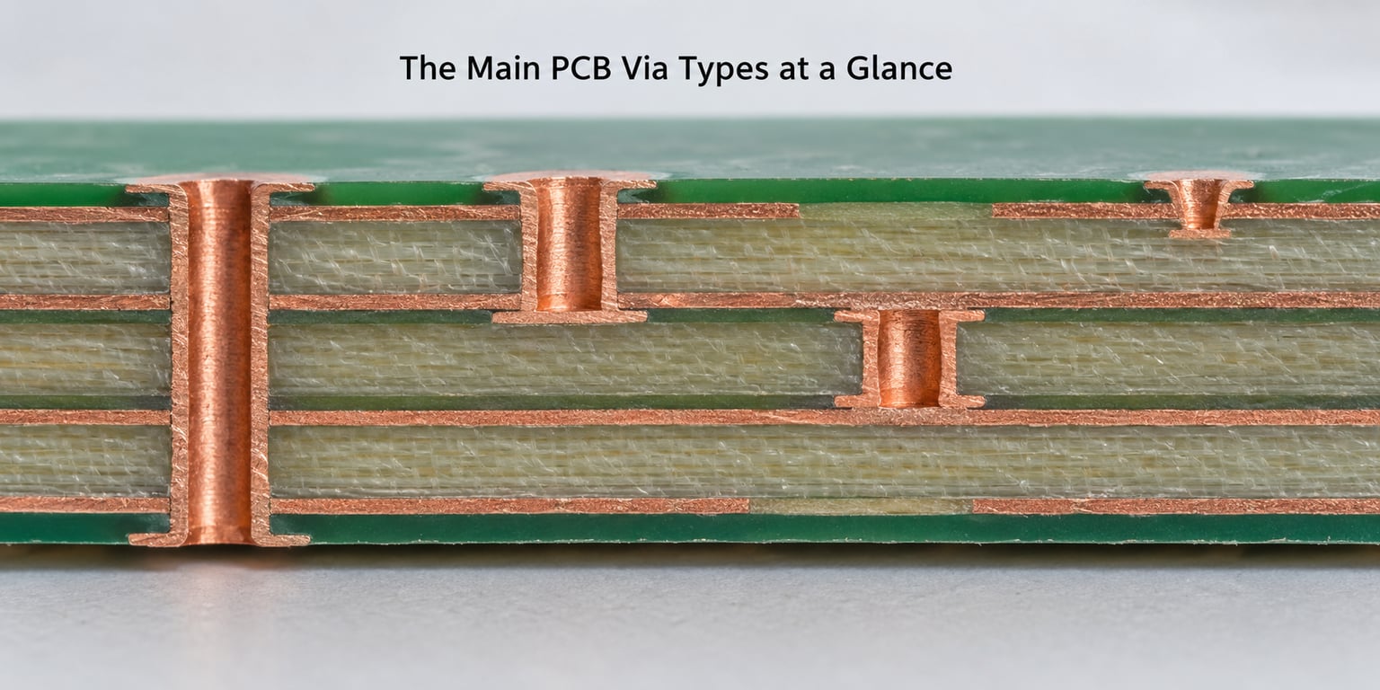
PCB via types explained side by side
The table below compares the five via constructions most designers meet. Sizes are finished hole diameters you will see quoted in a fabricator’s capability sheet, and cost is relative to a through via rather than a quoted figure.
| Via type | Starts on | Ends on | Drilled by | Typical size | Relative cost | Primary use |
|---|---|---|---|---|---|---|
| Through via | Top (outer) layer | Bottom (outer) layer | Mechanical drill | 0.2-0.8 mm / 8-32 mil | 1x baseline | General routing and inter-layer connection |
| Blind via | Outer layer | Inner layer | Laser | 0.1-0.2 mm / 4-8 mil | 2-3x | Routing between an outer and one inner layer |
| Buried via | Inner layer | Inner layer | Laser | 0.1-0.2 mm / 4-8 mil | 2-3x | Internal signal and power connections |
| Microvia | Any layer | Adjacent layer | Laser | 0.05-0.1 mm / 2-4 mil | 4-6x | High-density interconnect and BGA fan-out |
| Mechanical via | n/a | n/a | Mechanical, not plated | 1-6 mm, hole size chosen by purpose | Negligible | Mounting, tooling and alignment holes |
Read the Start and End columns together. A through via is the only row that starts and finishes on two outer layers, and that single fact explains most of its behaviour electrically and mechanically.
Through Vias: The Standard Connection Between PCB Layers
A through via is mechanically drilled from one face of the board to the other after the stack-up is fully laminated, then plated. It carries a pad on every layer it passes and an antipad on every plane layer, which is what keeps a signal via from shorting into a ground plane.
The practical mechanical floor is around 0.15 mm / 6 mil finished hole on mainstream capability, with 0.2-0.8 mm / 8-32 mil being the range most designers settle on. Barrel plating is commonly around 0.025 mm / 1 mil of copper, and a typical via contributes roughly 1-2 pF of parasitic capacitance.
Use through vias when routing room exists. They are the cheapest option, they can be drilled and plated in one pass, and their mechanical strength is not in question. The two costs are the antipad they punch through every plane layer, and the barrel that continues past the last layer you actually connect to.
That leftover length is called a stub, and on a thick board it can be longer than the useful part of the connection.
Blind Vias: Connecting Selected Inner Layers
A blind via starts on an outer layer and stops on an inner layer. It is laser-drilled so the depth is controlled, and it has its own drill file entry with a defined stop depth rather than passing through the whole board.
The win is spatial. A blind via only creates an antipad on the layers it actually spans, so freeing a ground or power plane from a hole it did not need. On dense multilayer designs that recovered routing area is often the reason the design fits at all.
Use it when a signal needs to reach an inner layer and should not disturb the planes on the far side. Keep the depth in your fabricator’s stated range; blind via aspect ratio guidance commonly sits around 1:1, and deep blind holes reduce plating reliability.
Buried Vias: Internal Connections Without Outer Access
A buried via starts on one inner layer and ends on another, so it is invisible from both outer surfaces. You cannot see it, probe it, or test it with a flying probe from outside, which is the practical reason it exists: inner-layer routing without breaking the outer surfaces.
A blind via and a buried via use the same fabrication process; they differ only in which layers they start and end on. Both are laser-drilled and plated during a sequential lamination cycle, and both are quoted in the same cost class.
Use buried vias for internal signal and power distribution in a stack-up where the outer layers must stay clean, for example a return path or a decoupling connection that lives entirely between signal layers.
Microvias: Small Vias for Dense PCB Designs
A microvia is a laser-drilled hole in the 0.05-0.1 mm / 2-4 mil range that spans one adjacent layer pair. It is the building block of build-up technology, where fine lines are added to a core in successive lamination cycles, which is how smartphone-class boards reach that density.
There are two common arrangements. A stacked microvia puts two or more microvias directly on top of each other, each one spanning a different layer pair, which saves horizontal area at the cost of more process steps and lower yield. A skip via spans two layers rather than one, and is only practical where the dielectric between them is unusually thin.
Drill size sets the limit here. A smaller hole holds less plating, so the aspect ratio window is tight, commonly quoted around 1:1 for laser microvias, and registration between layers has to be controlled precisely.
What via-in-pad changes
A via-in-pad places a microvia or via directly inside a component land, typically a BGA pad, so the connection drops straight from the ball to the inner layer. The known failure mode is solder siphoning: during reflow, molten solder wicks down the open barrel and the joint comes out dry.
The standard fix is to fill the barrel with non-conductive epoxy, planarize it flat, plate copper over the top, and tent or cap the far side so no open hole remains. Under a fine-pitch BGA the surface also has to be flat enough for the ball to seat, which is why the filled and capped process matters as much as the via geometry.
Mechanical Vias: When the Hole Serves More Than an Electrical Purpose
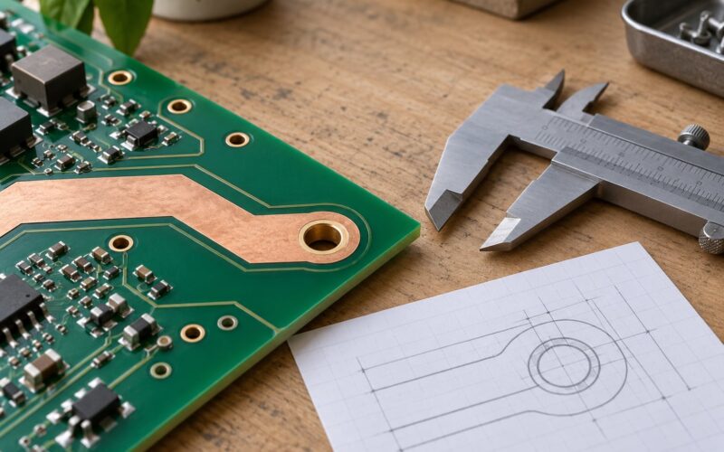
Not every hole on a PCB is a via. Mechanical vias — mounting holes, tooling holes, alignment holes for pick-and-place fiducials — exist for mechanical reasons and are usually left unplated, or plated only if the customer needs the copper.
The distinction is simple: an electrical via has a plated barrel and a pad, and a mechanical hole does not. Unplated holes in a ground pour still show up as voids in that plane, so a non-plated mounting hole sitting inside a large copper region can disturb the very plane you were trying to keep solid.
Two rules keep them from causing trouble. Keep mounting holes away from high-current and high-speed paths, since a hole edge is a stress concentration in the laminate. And check the board’s mounting hole positions against your enclosure tolerances early, because changing them after routing is finished means a respin.
How PCB Via Types Affect Electrical Performance
Every via is a discontinuity in the transmission line. It adds inductance, adds a small capacitance, and — the part that matters most at speed — it changes the return path.
Resistance and current capacity
Via resistance scales with resistivity, length, and the inverse of the cross-section of the copper barrel, so the practical levers are a larger diameter, thicker plating, and a shorter barrel. For copper at roughly 20 degrees C, a common approximation is 0.5 milliohms per via with a 0.25 mm / 10 mil finished hole and standard plating, rising quickly as the hole shrinks or the barrel lengthens.
A rough sense of scale: a 0.3 mm / 12 mil via is commonly in the low single-digit amps range before you start derating for temperature rise and the surrounding laminate. When you need more current or more heat spreading, parallel vias are the normal answer — four or nine small vias in a grid do the job of one large one that would not fit anyway.
Thermal vias follow the same logic. A grid of small vias under a hot device pulls heat into an inner plane, and filling them improves the path considerably.
Stubs and signal integrity
Connect a signal from L1 to L3 in a sixteen-layer board and the through via keeps going to L16. The barrel beyond L3 is a stub: a length of transmission line that ends in an open, and an open reflects.
That is the mechanism behind stub resonance on high-speed links. The fix list runs from cheapest to most effective: shorten the barrel with a blind or buried via, then microvias, then back-drill the unused length, and finally add stitching vias around the signal via so the return path stays continuous and the fields stay contained.
Two habits help regardless of via type. Keep the reference plane unbroken under the transition, and place a ground via close to every signal via that changes layer.
How to Choose the Right PCB Via Type
Start from the constraint that hurts most, not from the most capable option. In practice that is a short decision:
- Generous routing room, modest layer count — through vias. Cheapest, drilled in one pass, no special capability needed.
- Dense multilayer with a high pin-count BGA — blind and buried vias, to recover routing area and keep planes intact.
- Fine-pitch BGA or HDI-class density — microvias, usually stacked and usually via-in-pad with filled and capped barrels.
- High-speed backplane or long links — short blind or buried transitions, or through vias with the unused length back-drilled.
- High current or a hot device — multiple parallel through vias in an array, often filled for thermal path.
- Mounting and alignment — mechanical, unplated holes placed away from sensitive paths.
Relative cost, in broad tiers: through vias sit at the baseline, blind and buried vias commonly land around two to three times that, and microvia-heavy build-ups around four to six times. Ask for each via type as a separate line item on the quote, because a design that leans on buried vias can be repriced around them alone.
Fabricator capability checklist
Send these to the shop before you release files, not after:
- Minimum mechanical drill and minimum laser drill
- Maximum aspect ratio for through holes and for blind or buried vias
- Whether they run sequential lamination, and how many cycles the stack-up needs
- Fill and cap process availability, including epoxy and conductive fill
- Laser drill registration and the layer counts they support
- Per-via-type pricing, and whether inspection includes X-ray for inner vias
Engineers get burned by this most often at the capability end rather than the price end: the shop’s aspect ratio limit is tighter than assumed, and the stack-up has to be redesigned late.
Manufacturing and Design Considerations for PCB Vias
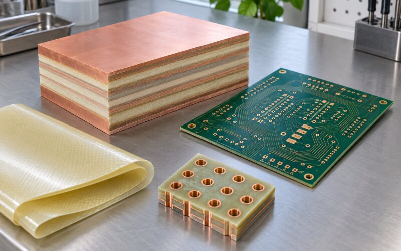
Understanding the build explains every capability difference above. A conventional build drills and plates all through-holes after the board is fully laminated. A sequential build laminates a layer pair, drills and plates the blind, buried or microvias in it, then adds the next pair — which is why those vias cost more and take longer.
Mechanical drilling cuts a straight hole and is fast, but it has a practical floor set by drill wander and tool life. Laser drilling vaporises the copper and burns the dielectric, which leaves a characteristic tapered pit in the copper barrel rather than a straight wall. The plating has to cover that taper, and layer-to-layer registration has to be tight enough that a microvia lands where the design says it does.
After drilling comes micro-etching and seeding, copper electroplating into the barrel, debris removal, then imaging and etching of the pads. Barrel plating is the step that decides whether the via conducts, so fabricators that quote a plating thickness are quoting something real.
Design rules worth writing into your library
- Aspect ratio — board thickness divided by finished hole diameter. Common guidance is at or below 10:1 for mechanical through-holes, around 1:1 for blind vias, and up to roughly 1:12 quoted for some buried via capability. Treat these as typical capability figures, not a standard.
- Annular ring — the copper ring left around the drilled hole after drilling, typically 0.05-0.1 mm of minimum ring width. This is what you are really protecting when you set a pad-to-drill ratio.
- Pad-to-drill — pad diameter larger than finished hole by a defined amount so the ring survives drilling tolerance.
- Spacing — keep via-to-via centres at least about twice the via diameter, and give plane layers antipad clearance so the barrel is properly isolated.
- Tenting — solder mask covers vias that are not used as a component pin, which keeps debris and solder out of the barrel. Any via you intend to solder into should be left open.
- Filling and capping — epoxy fill is used for insulation, planarization and to stop solder siphoning; a metal or conductive fill adds thermal and shielding behaviour. Unfilled laser-drilled blind and buried barrels can also trap air and voids, which hurts reliability under thermal shock, so filling is sometimes a reliability requirement rather than a cosmetic one.
- Landless vias — a trace enters the hole with no pad at all, maximising routing density at the cost of manufacturing margin. Useful, and not a default.
- Drill file — every via type you use needs its own coordinate and depth definition in the drill data. Free or submitted vias still need the fabricator to know what they are.
One limit is worth stating plainly: blind and buried vias cannot be visually inspected from the surface. Verification relies on electrical continuity test, and X-ray imaging when a fab or customer needs positive confirmation of the barrel.
Glossary
Pad — the copper landing where a trace meets a via. Antipad — the clearance void isolating a barrel from a plane. Annular ring — copper ring remaining after drilling. Barrel — the plated wall of the hole. Drill file — the manufacturing file defining hole positions and depths per via type. Aspect ratio — board thickness over finished hole diameter. Tenting — masking over an unused via. Planarization — shaving a filled via flat. Via stub — unused barrel beyond the last connected layer.
Common Misconceptions About PCB Via Types
“Blind and buried vias are different technologies.” They are the same process. Only the start and end layers differ, so they also share cost, capability limits and inspection method.
“A laser-drilled hole is plated all the way through automatically.” No. The barrel is plated to the depth the hole was stopped at, which is why depth control is the fabricator’s core skill on these builds.
“Any via can be drilled anywhere on any layer.” Inner layers are not accessible until that layer pair is exposed, so an inner-to-inner connection requires a sequential build rather than a single pass.
“Aspect ratio limits are standards.” The 10:1 and 1:12 figures you see quoted are typical capability numbers from fabricators, not a specification you can rely on without checking. The shop’s DFM report is authoritative.
“Every via needs filling or capping.” Most signal vias do not. Filling is used for via-in-pad, thermal vias, shielding, and where thermal-shock reliability demands it.
“A plated hole and a via are the same thing.” Not quite. A component plated through-hole is plated only after full lamination, while a via is plated as part of the layer build — which is why the same word gets used loosely in conversation.
Frequently Asked Questions
What are the types of vias?
The four main via types are through vias, which connect the top and bottom layers; blind vias, which connect an outer layer to an inner layer; buried vias, which connect two inner layers; and microvias, which laser-drill between adjacent layers. Stacked microvias, via-in-pad, back-drilled, filled and capped, and tented vias are variants built from those four. Mechanical mounting and alignment holes are not electrical vias.
Are blind and buried vias the same thing?
They are made the same way and differ only in where they start and end. A blind via runs from an outer layer to an inner layer, so you can see its opening on the board surface. A buried via runs from one inner layer to another and is invisible from both sides. Both are laser-drilled and plated during a sequential lamination cycle, and both usually sit in the same cost tier.
What is a microvia and how is it different from a through via?
A microvia is a laser-drilled hole of roughly 0.05 to 0.1 mm finished diameter that spans one adjacent layer pair. A through via is mechanically drilled, usually 0.2 to 0.8 mm, and passes the full thickness of the board with a pad on every layer. Microvias support far higher routing density, tolerate a much tighter aspect ratio, and cost several times more than a through via.
What is via-in-pad and why does it cause solder problems?
A via-in-pad puts a via inside a component land, usually under a BGA ball, so the connection reaches an inner layer without horizontal routing. The risk is solder siphoning: during reflow, molten solder wicks down the open barrel and leaves a dry joint. The fix is to fill the via with non-conductive epoxy, planarize it flat, plate over the top, and tent or cap the far side.
What is a via stub and how do you remove it?
A via stub is the unused length of barrel beyond the last layer a via actually connects. On a signal transition it behaves as an open-ended transmission line and reflects energy back, which shows up as ringing. Remove it by ending the via on the layer you need with a blind or buried via, using microvias, or by back-drilling the leftover length. Keeping a ground via near the signal via helps the return path.
Why are blind and buried vias more expensive than through vias?
Because they require a different build. Through vias are drilled and plated in a single pass after full lamination. Blind and buried vias are laser-drilled and plated layer-pair by layer-pair during a sequential lamination cycle, each with its own drill file and defined stop depth. Multiple lamination presses, more process steps and X-ray verification all add time, and fabricators that lack the capability cannot quote the build at all.
Conclusion: Start With the Simplest Via That Meets the Design
Use ordinary through vias unless routing density, impedance control, a package’s construction or a mechanical need forces something else. Blind and buried vias buy back plane area and routing channels, microvias buy density, and back-drilled vias buy signal integrity — each one at a cost in money, process steps and fabricator capability.
Because capability limits move between shops and change over time, agree the stack-up and the via types with your fabricator before you freeze the design, and send the capability checklist above with the RFQ. The stack-up is a joint decision between you and the shop that builds it, not a detail you settle afterwards.