Most PCB design mistakes to avoid are not exotic. They are the same handful of oversights that turn a clean schematic into a board that will not power up, will not enumerate over USB, or runs too hot to touch: a footprint that does not match the datasheet, a ground plane that stops at a seam, a 6 mil trace asked to carry 3 amps, and a design rule check that never ran. Every one of those is cheap to catch before release and expensive to catch after.
This list covers the full path a board travels, from schematic capture to the first bring-up. Each mistake gets the symptom you would actually see, the mechanism behind it, and the fix you can apply in your own tool. It is written for hardware and layout engineers, and for makers prototyping in KiCad or Altium who currently find out about these things from a forum post after paying for boards twice.
Table of Contents
- 12 PCB Design Mistakes to Avoid at a Glance
- 1. Ignoring the PCB Design Rules for the Manufacturer
- 2. Designing Without a Complete Netlist and Design Rule Check
- 3. Poor Grounding and Return-Path Design
- 4. Inadequate Power and Decoupling Layout
- 5. Ignoring Thermal Management
- 6. Using the Wrong Footprints or Package Land Patterns
- 7. Creating Signal-Integrity Problems
- 8. Failing to Plan for Electromagnetic Compatibility
- 9. Designing for Human Assembly Instead of Manufacturing Reality
- 10. Neglecting Mechanical Constraints
- 11. Skipping Fabrication and Assembly Documentation
- 12. Sending the Design Without a Final Design Review
- Frequently Asked Questions
- What is the 3H rule in PCB design?
- What is the 3W rule for PCB design?
- What are common PCB problems?
- Which PCB is the most toxic?
- How do I check my PCB design before sending it to fabrication?
- Why does my PCB get hot near the regulator?
- Where to Start on Your Next Board
12 PCB Design Mistakes to Avoid at a Glance
The table below is the whole article in one view. Every row is a mistake that survives review because it looks reasonable on screen, paired with what it does to the finished board and the correction that prevents it.
| # | Mistake | Failure mode | Likely consequence | Primary fix |
|---|---|---|---|---|
| 1 | Ignoring the fabricator’s design rules | Traces and annular rings below process capability | Drill breakout, open circuits, scrapped panel | Build rules from the capability chart, not from habit |
| 2 | No verified netlist and no DRC | Unconnected or unconnected-by-accident pins | Board assembles and does nothing | Netlist compare plus a clean DRC report |
| 3 | Poor ground and return-path design | Split planes, displaced return current | Noise, resets, unstable measurements | One solid ground plane, stitched, never cut |
| 4 | Inadequate power and decoupling layout | Long supply loops, caps too far from pins | Supply ring, brownout resets, EMI | Shortest possible loop, 100 nF at every supply pin |
| 5 | Ignoring thermal management | No copper, via, or sink path from a hot device | Board gets hot, device fails early in the field | Copper pour, thermal via array, component spacing |
| 6 | Wrong footprint or land pattern | Pin 1 mismatch, missing exposed pad | Part does not fit, shorts, no heat path | Verify against the datasheet drawing, measure it |
| 7 | Signal integrity ignored | Unterminated stubs, no reference plane, mismatched pairs | Reflections, ringing, link fails at speed | Continuous reference, no stubs, length matched |
| 8 | No EMC plan | Big loop areas, cables as antennas, no filtering | Emissions and immunity test failures | Tighten loops, filter at the connector, bond the chassis |
| 9 | Designed for human assembly, not manufacturing | No polarity marks, courtyards overlap, edge too tight | Assembler guesses, misplacement, bad joints | Follow the assembler’s guidelines, mark polarity |
| 10 | Mechanical constraints neglected | Holes off-grid, connector into the enclosure wall | Board does not fit or cannot be screwed down | Fit-check in CAD against the real enclosure |
| 11 | Fabrication and assembly documentation missing | No stackup, no drill table, no polarity notes | House defaults used, impedance wrong | Write the fab notes and assembly drawing yourself |
| 12 | No final design review before release | Gerbers shipped unreviewed | A full re-spin, days to weeks lost | Run a sign-off gate with a named owner |
The same failures also read backwards from the bench. This second table starts from what you observe on a dead or unstable board and maps it to the most likely layout cause, so you can diagnose without guessing.
| Symptom | Most likely cause | Mistake | How to verify |
|---|---|---|---|
| Board will not power up at all | Short between rails from a bridging solder mask or a bad footprint | 6, 9 | Check resistance rail to rail with the board unpowered |
| Board gets very hot on power-up | Regulator output shorted, or no thermal path under a switching device | 5, 6 | Measure current at the connector; compare to the expected quiescent draw |
| Browns out or resets under load | Undersized supply trace, decoupling too far from the pin | 4 | Scope the supply rail at the device pin, not at the connector |
| USB or Ethernet will not enumerate | Return path interrupted, pair length mismatch, missing series damping | 3, 7 | Check for plane seams under the pair; confirm the pair is on one continuous layer |
| Erratic readings on an analog front end | Digital return current crossing the analog ground region | 3, 8 | Move the analog reference to a quiet corner, add a guard trace |
| Open traces or pads after reflow | Annular ring too thin for the drill, or pad-to-drill ratio too small | 1, 5 | Compare pad and drill against the fabricator’s table |
| Radio performance drifts after a minute | Supply ripple or a self-heating loop near the amplifier | 4, 5 | Scope the supply while transmitting; watch junction heat creep |
| Board works on the bench, fails in the enclosure | Cable antenna, no chassis bond, panel resonances | 8, 10 | Re-test inside the enclosure with the lid closed |
1. Ignoring the PCB Design Rules for the Manufacturer
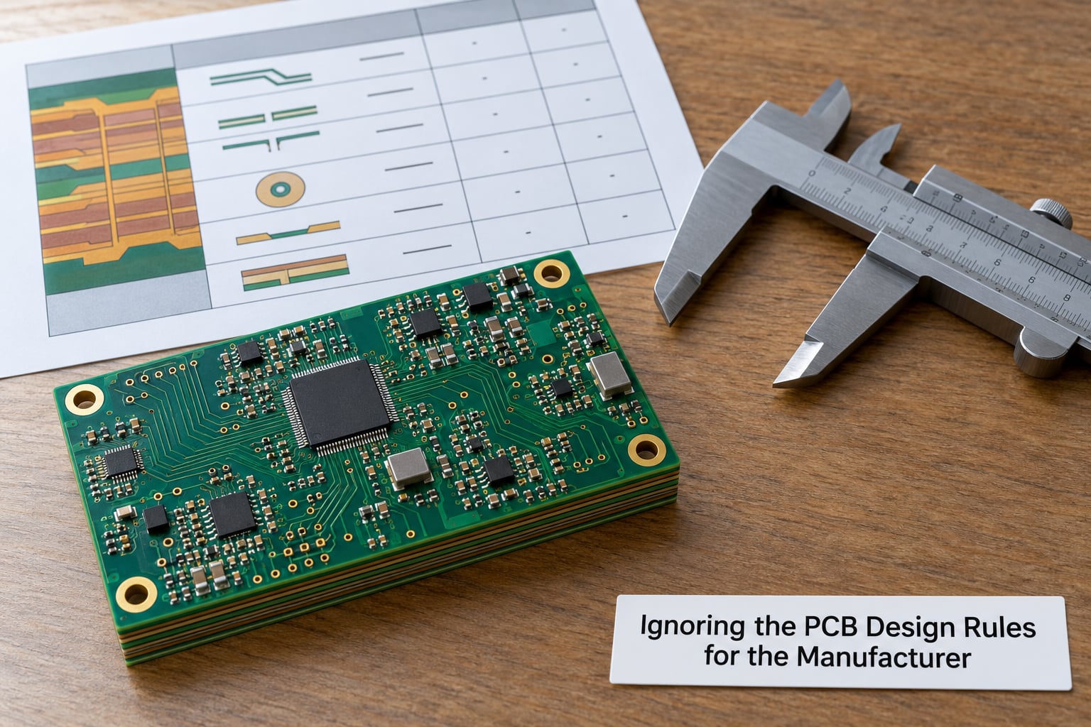
The single most damaging assumption is that the defaults in your EDA tool match the process that will actually etch the copper. They usually do not, and the gap shows up as drill breakout, copper that thins below spec, or solder mask dams that the fabricator cannot hold.
Every fabricator publishes a capability chart. It lists minimum trace width and spacing, minimum annular ring, drill tolerances, minimum solder mask dam, minimum silkscreen line width, aspect ratio limits, and the surface finish and copper weight available. Those numbers, not the ones in a default constraint file, define what will survive the process.
Concretely: a 10 mil pad with a 20 mil drill leaves a 5 mil annular ring on each side. If the fabricator’s minimum annular ring is 4 mil, you are inside capability. If it is 6 mil, that pad breaks out on the next drill hit, and you have a board with an open connection that costs a full re-spin to fix. The pad looked completely normal on screen, which is exactly why it slipped through.
Two related limits get missed just as often. The first is aspect ratio, which is drill diameter to finished board thickness. A 0.2 mm hole through a 3.2 mm board is an aspect ratio of 16 to 1, and many standard processes struggle above 10 to 1 because copper plating inside a long hole is harder to control. The second is the pad-to-drill ratio, which governs whether solder wicks the entire pad away during reflow, leaving an open joint that only fails in the field.
The fix takes an hour. Request the capability chart for the specific process and price tier you have quoted, then build your design rule constraint file from it, not from a template. Set minimum widths to the fabricator’s numbers with a margin, and run DRC against that file. For hobbyist and volume boards alike, this is the difference between a rule you believe and a rule that is true for your part number.
2. Designing Without a Complete Netlist and Design Rule Check
A DRC run is worthless if the underlying netlist is wrong, and the netlist is where a lot of silent failures live. Missing nets, duplicated reference designators, nets that go nowhere, and mismatched footprints between schematic and layout all pass a clean DRC because the tool checks internal consistency, not intent.
Design rule check verifies that the copper you drew matches the constraints you set. It cannot tell you that a power symbol landed on a signal net, that two different connectors share a pin number, or that the schematic says 10 connections and the layout has 9. Those come from comparing the schematic against the layout directly, and from reading the netlist with a suspicious eye.
Use a netlist comparison step. Most tools can export the layout netlist and diff it against the schematic netlist, and the report should be empty apart from intentional differences. Then read the netlist itself for a few specific smells: nets with exactly one connection, power nets with no specified source, and any net named for a signal that is actually a ground return.
That last one deserves emphasis because it is so common. Routing every net to a two-pin header because it is convenient produces a board with a large number of short stubs, and each stub is a discontinuity for anything fast. Practitioners who post their failures to r/PCB and the DigiKey forum usually have the opposite problem, where nets that should be tied together never got merged because the schematic used two different ground symbols and the tool did not flag it.
The routine that catches all of this is short: update the PCB from the schematic, run the netlist comparison and require zero unexplained differences, run DRC and require zero errors, then open a handful of pins by hand and confirm the connection exists. Ten minutes now replaces a week of board swaps later.
3. Poor Grounding and Return-Path Design
A ground symbol on a schematic tells you nothing useful. What matters is whether every current has a short, low-inductance path back to its source on the same layer it left, and the most common failure in this whole list is a return current that has to go around something to get home.
Splitting the ground plane under an analog and digital partition is the classic version. The theory is that separating the two grounds keeps digital noise out of the analog reference. In practice, the return current for a signal crossing the split has to detour around the seam, and that detour makes the trace act as an antenna radiating into your analog front end. A solid, uninterrupted ground plane with careful partitioning of the signals themselves is the better approach. If you need a genuinely separate analog ground, the answer is a carefully placed, low-impedance tie point, not a full-length cut.
The same mechanism explains a surprising number of failures. A USB link works with an antenna hanging off the end, then fails in the enclosure because the enclosure changed the ground return and added a resonant structure. A sensor reads cleanly on the bench and drifts when the motor spins up because the motor return current now shares a path with the sensor reference. Both are return path problems wearing a different name.
Loop area is the underlying measure. Every current loop, whether it is a high di/dt switching loop or a signal and its return, has inductance proportional to the area it encloses. Halving the area halves the inductance, and the radiated and coupled noise drops with it. This is why a switching regulator’s input capacitor sits on the opposite side of the package from its input pin, and why the freewheeling diode goes on the same side as the switch.
On a multilayer board, the return path under a signal on the outer layer is the solid plane on the adjacent inner layer. Keep it continuous. Stitch ground planes together with a dense array of vias wherever the two ground layers must behave as one, and never route a signal over a split, a void, or a keepout on its reference layer. One missing ground under a fast edge is enough to ruin it.
4. Inadequate Power and Decoupling Layout
Power layout fails in two ways: the supply path is too long or too thin to deliver what the device demands, or the local energy a switching device needs is not stored close enough to it. Both show up as brownout resets that vanish when the load is light, which makes them hard to reproduce.
Trace width for current is the first of these. A widely used starting point in the IPC world is the 20/10/5 rule: roughly 20 mil of external trace handles around 1 amp, 10 mil handles about half that, and 5 mil around a quarter amp, for a typical 1 oz copper and modest temperature rise. Treat those as a starting point rather than a law, because the real number depends on copper weight, board thickness, allowed temperature rise, and how long the trace runs. For anything above a couple of amps, use copper pours or planes rather than traces at all, and remember that internal layers carry heat away much better than the outer ones.
Decoupling is the second. The rule of thumb that covers most digital parts: one bulk capacitor, typically 1 to 10 uF, at the entry to each supply rail, and one 100 nF ceramic at every supply pin, placed as close to that pin as the layout allows, with the ground connection shorter than or equal to the supply connection. That capacitor plus the pin forms a small loop, and small loop equals small inductance, which is the whole point.
Getting this wrong is easy because the schematic looks identical either way. The datasheet decoupling requirement is drawn with a capacitor symbol near the pin, and the layout tool will happily place that capacitor in the middle of the board because the electrical connection is satisfied. The decoupling does nothing useful at 50 mm. The high-frequency current goes to the nearest low-impedance return, which is the plane, and the loop it forms is large and inductive.
Watch the capacitor type too. A 100 nF X7R or X5R ceramic is effective far into the gigahertz range, while older high-capacitance technologies lose their effectiveness as frequency rises. A common failure is a board that is stable with the power supply connected and oscillates when it runs from a battery, because the lab supply was quietly supplying the transient that the board cannot produce for itself.
5. Ignoring Thermal Management
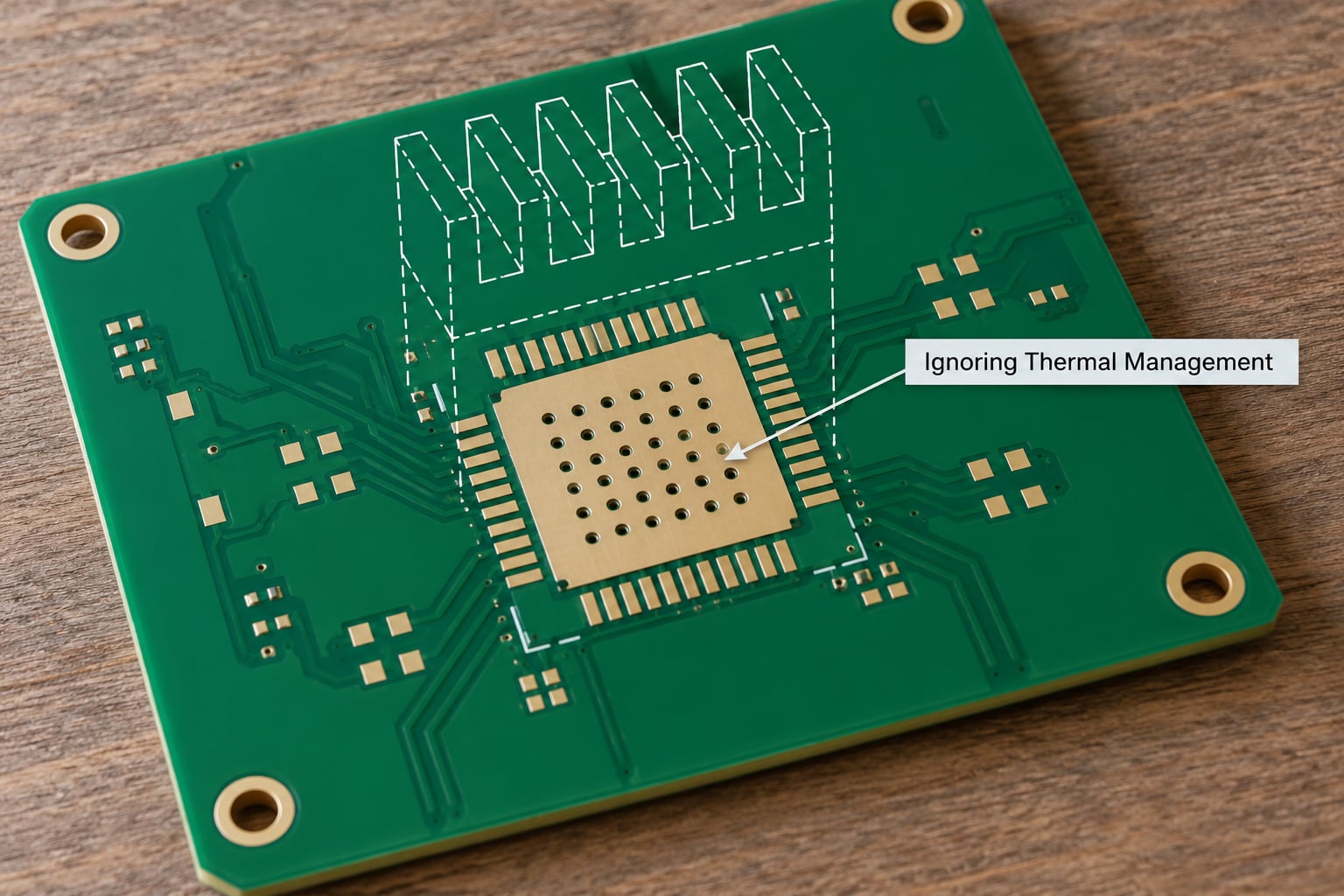
Every component that dissipates power has a junction temperature, and the gap between that temperature and the ambient decides how long the part lives. A design with no deliberate thermal path will work on the bench and fail in the enclosure, where the airflow you had disappears and the ambient rises.
Heat leaves a device through three paths: through its leads, through the exposed pad or heat spreader underneath, and through the air. On a board, only the second one is under your control. Copper pours conduct heat, vias move it between layers, and a heat sink or spreader moves it into the air. A device with an exposed pad soldered to nothing but a thin thermal relief pad on an otherwise empty board has almost no thermal path, and that pad exists in the footprint for a reason.
Thermals vias are the main tool. A via under a QFN or a power stage in a tight array, filled or tented depending on the fabricator, connects the top-side heat pad to the ground or a dedicated thermal plane underneath, and to the bottom copper where a heat sink can sit. Two rules matter. Do not place thermal vias in the signal escape paths of a fine-pitch package, because they have to share the same space as the signal fanout, and decide early whether the vias will be filled, because that is a different and more expensive process.
A concrete example: a 3 A switching regulator in a DFN package placed next to the board edge with a 5 mm copper pour and no vias. It will work, run warm, and reach a junction temperature high enough to trigger thermal limiting within minutes of load. The same part on a pour with a 4 by 4 thermal via array and a heat sink footprint for a 12 mm clip dissipates into the copper instead of into a small patch of FR-4, and the difference is the difference between a product that ships and one that comes back.
Component spacing is the cheapest part of this. Nothing next to a hot device can cool itself, so keep inductors, temperature sensors, and precision parts out of the rising air above a power stage. If the enclosure is sealed, assume less airflow than you measured on the open bench, and design for that number.
6. Using the Wrong Footprints or Package Land Patterns
Footprint mistakes are the most expensive kind, because they are usually not detectable until someone tries to place the part or until a bare board is checked with a microscope. And they frequently look correct, because a library footprint for the wrong variant looks a lot like the one you need.
The usual causes are a library footprint that was never verified, a part number that resolves to a different package variant than the one on your BOM, a pin 1 marker that does not match the datasheet drawing, and an exposed pad that was deleted because it was a separate symbol in the schematic.
A concrete comparison makes this tangible. Two resistor packages, one 0402 imperial and one 1005 metric, differ by well under a millimeter in body length. Their land patterns are not interchangeable in a meaningful sense, and a pad built to the 1005 drawing can be invisible under a 0402 body, leaving the part floating with no solder to attach it to. The reverse case, a 0402 pattern on a 1005 part, gives a part that sits with its ends off the copper and does not solder at all. Neither failure gives you a warning during DRC.
The fixes are unglamorous and effective. Read the recommended land pattern from the manufacturer’s datasheet, not from a community library, and compare pad dimensions, tolerances, solder mask expansion, paste aperture, and the silkscreen outline. For any exposed pad, paste windows matter as much as the pad: paste it in windows rather than one solid aperture so reflow does not void the centre, and drill thermal vias inside the pad footprint. Then print the board at 1:1 on paper and lay the actual components on it. It takes twenty minutes and it catches nearly every mechanical footprint error before a single board is cut.
Also check the courtyard, the keepout area around the component defined in IPC-7351. Overlapping courtyards do not trip a copper DRC but they predict that two parts cannot physically be placed side by side, which is exactly the assembly failure the package exists to prevent.
7. Creating Signal-Integrity Problems
Signal integrity problems are geometry problems. At low enough frequency, a trace is a wire. Above roughly a tenth of the rise time of your signal, the trace is a transmission line with a characteristic impedance, and the board around it becomes part of the circuit.
Continuous reference is the first requirement. A signal on the outer layer uses the inner plane beneath it as its return path, and that return only exists where the plane is there. A plane void, a split, a routed slot, or a dense via field with almost no copper left between the holes all interrupt it, and an interrupted return current forces the current to flow around the obstacle, adding inductance and radiating. The fix is either to route the signal where its reference is intact, or to fill the void with stitching vias, ideally at less than a quarter wavelength of the signal’s rise time.
Vias are the second. A via on a high-speed net adds a stub: a short piece of trace that terminates in an unterminated via barrel, which acts as an antenna and a resonator at the frequency where its quarter-wave length matters. Back-drilled vias remove most of the stub, but the cheap fix is usually fine on its own. If a layer change is unavoidable, put the via close to the signal’s source or destination, keep the signal on one layer for as much of its run as you can, and avoid via stubs entirely. A series termination resistor, usually 22 to 33 ohms, at the driver often fixes a ringing edge that no amount of layout tweaking improved.
Differential pairs are the third. Keep the two traces of a pair the same width, the same distance to the reference plane, and matched in length, and route them over an unbroken reference. Most tools will report length mismatch, and the tolerance you can accept depends on how much skew your receiver tolerates: a few mils on USB 2.0, single-digit mils on USB 3 and Ethernet, and sometimes under a millimetre on the newest memory interfaces. Pair symmetry also matters more than most beginners expect, because a mismatch in one trace’s distance to the plane changes its impedance and unbalances the differential mode.
Do the math before routing. A microstrip’s impedance depends on trace width, copper thickness, and the dielectric constant and thickness of the layer beneath it. If the fabricator is not given a stackup and an impedance target, the board comes out with whatever impedance the process naturally produces, which is not the number you designed for. The 8 mil rule of thumb, 8 mil of trace to 8 mil of gap, produces roughly 50 ohms on common 4-layer material and is a decent sanity check that the stackup you asked for is plausible.
8. Failing to Plan for Electromagnetic Compatibility
EMC problems are usually current loops and cables, in that order, and both are decided by layout decisions made long before anyone measures anything. A small controller board with a two-wire cable leaving the board is the standard example: if those two wires pick up common mode current and then radiate, no amount of filtering inside the box will fully fix it.
Keep the loop areas small, and that includes the loop formed by a cable. A long paired run with a big area between the conductors acts as a receiving antenna for anything inside the enclosure. Tighten the circuit that drives it, add a common mode choke or a ferrite at the connector where the cable leaves the board, and terminate the shield properly. Filtering belongs at the connector, not scattered across the board, because that is the only point where the noise actually enters the enclosure.
Give the enclosure a ground reference and bond it. A metal enclosure that is floating picks up whatever common mode current the cable imposes, and the enclosure then radiates more than the board ever would. Bond the chassis to the signal ground with a defined, low-impedance connection, using multiple vias or a dedicated connection near the entry point, and be deliberate about the return path for shield currents.
Watch the board edges. A trace running to the edge of the board can couple to its neighbour on the far side of the enclosure, and a long trace on the outer layer is an antenna at the frequencies where its length is a meaningful fraction of a wavelength. Ground guard traces help on dense analog sections, and orthogonal crossings between adjacent layers help in dense digital sections, since parallel runs between two planes couple far more strongly.
Plan the test, not just the fix. If the product has a compliance requirement, find out the limit before the layout, because some radiated emission problems are cheaper to design out and prohibitively expensive to fix later with shielding tape. Consider a pre-compliance scan in a small chamber before committing to a design, and keep the cables in their final configuration, since a passing measurement with the cables coiled is worth very little.
9. Designing for Human Assembly Instead of Manufacturing Reality
Designing for a human who is holding the board in a vise is a different discipline from designing for a pick-and-place machine and a reflow oven, and boards are almost always assembled by both. Polarity markings, silkscreen legibility, courtyard clearances, test access, and fiducials are all assembly-side decisions, and every one of them is usually made by accident if nobody makes them deliberately.
Mark polarity and pin 1 explicitly on the silkscreen, next to the part, with a marking that survives the process. A part number printed on the board tells the operator nothing about which way round a polarized capacitor goes, and a large ground pour on the back of a tantalum or an electrolytic can swallow the silkscreen line entirely. Keep the silkscreen clear of pads and of exposed thermal pads, and if the tool will not let you move it, move the pad.
Respect the assembler’s rules. Component spacing has to accommodate the nozzle and the camera, and courtyards are how that gets expressed. Keep tall or heavy parts away from the board edge, where the depanelizing step and the handling jig work, and keep connectors and mechanical parts off the very edge so the tab that holds the panel together does not run through them. Check that the reflow profile can actually reach the highest thermal mass on the board without cooking the parts, and note any components that cannot go through a wash or cannot tolerate a second reflow pass.
Add test points before you need them and while the layout is still flexible. A ground pad, a few supply rails brought to a header or a pogo-pad footprint, and a couple of clock or reset lines will save an entire debugging session, and adding them later means a re-spin. Fiducials on both sides, exposed and un-masked, cost nothing and remove a whole category of setup problem at the assembler. If the board will be panelized, tell the fabricator the board is panelizable, supply the tooling holes and the breakaway tabs, and confirm the panel rails do not cut through a keepout that matters.
Order spares. This is the least technical item on the list and it shows up constantly in forum threads, because boards get destroyed by the exact mistake they were built to investigate. A prototype run is cheaper per board than a second run of one, and having three boards means a short across a rail during bring-up is an inconvenience rather than a schedule event.
10. Neglecting Mechanical Constraints
The board has to fit the box, and the box is a 3D CAD model that was finished long before the layout. Connector alignment, mounting hole position, board outline tolerance, keepouts, and component height are all layout constraints, and every one of them is invisible on a two-dimensional canvas.
USB connectors are the classic failure. A through-hole USB-C receptacle is usually placed on the board edge, which is correct, and it has a height and a mating clearance that the enclosure must clear. If the enclosure wall sits 2 mm above the connector face, the plug does not seat. The fix is to import the enclosure model into the PCB editor and check the mechanical fit, which any serious tool can do, and to verify the connector height against the actual mating cable and mating shell, not just the connector datasheet drawing.
Mounting holes are the other half. A 3.2 mm hole on a board with a different drill table comes out 3.4 mm and sits off-centre in a 3.2 mm standoff, so the screw does not pull flat. The same holes can act as tooling holes for panelization if the spacing matches the fabricator’s rails, so tell the fabricator what they are. Keep copper and plane areas away from the hole unless the drawing specifically calls for a plated mounting hole with a defined keepout ring, and remember that a large unplated hole near a power plane can split it.
Give the board an outline with a defined tolerance, and put a mechanical drawing on it. Include every component’s height in the check, not just the connectors, and remember that the tallest part is often a heat sink or a terminal block added late. Leave assembly clearance for the direction the board is inserted, and check that the panelization direction does not run a breakaway tab across a tall component.
11. Skipping Fabrication and Assembly Documentation
If you release Gerbers with no notes, the fabricator will use their house defaults for anything you did not specify, and their defaults will be reasonable for their most common board, not for yours. The places where this hurts most are the stackup, the impedance, the finish, and the mask definitions.
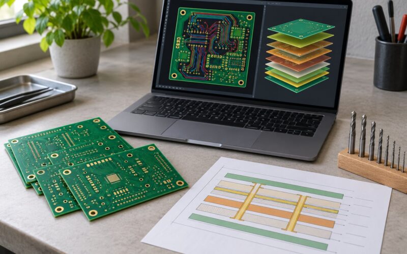
Specify the layer stackup with actual dielectric thicknesses and the material you want. Controlled impedance is calculated from that stackup and the fabricator’s process, so if the impedance target is not in the documentation, it will not be manufactured, and a board that needed 90 ohm differential will arrive at whatever the process naturally makes. Include the drill table, the finished board thickness and copper weight, the surface finish, the solder mask and silkscreen colours and legend side, the minimum and maximum drill and the plating requirement, and any nonstandard requirements such as filled vias, a thermal via tenting rule, or a controlled impedance coupon.
For assembly, provide a fabrication drawing or assembly drawing that shows the top and bottom with polarity marks, pin 1 indicators, and the component side, plus a BOM with manufacturer part numbers, a pick-and-place file with the correct rotation and side defined for every part, and an assembly drawing for anything hand placed. State the board’s cleanliness requirement if the application needs it, and give the assembler the test method: which points to probe, what readings to expect, and what a fail looks like.
Put test instructions in the release package, not in someone’s inbox. The person debugging a board three weeks from now will not remember what the 0.6 V on that rail is supposed to be, and a single page of expected measurements saves a support thread.
12. Sending the Design Without a Final Design Review
No single mistake is as expensive as releasing a design that nobody reviewed as a whole. Each mistake in this list is locally reasonable. The combination is what a review catches, and a review is a different activity from DRC, from netlist comparison, or from looking at the board yourself. Put a short, fixed sign-off checklist in front of the release, and make someone other than the designer sign it.
The gate, in order. Electrical intent: schematic reviewed by a second person, power trees reviewed for current and direction, all rails and their sources identified, netlist compared to the PCB with zero unexplained differences. Manufacturability: DRC clean, the design rule file built from the fabricator’s capability chart, no features below the process limits, stackup and impedance specified. Assembly: polarity and pin 1 marked, silkscreen clear of pads, courtyards clean, test points present, panelization reviewed. Mechanical: board outline, mounting holes, keepouts, and component heights fit-checked against the enclosure model. Release package: Gerbers, drill files, stackup, fab notes, assembly drawings, BOM, pick-and-place, and test instructions all present and consistent with each other.
After the first prototype, treat the board as a measurement, not a verdict. Write down what you had to change, because the second spin’s difference list is the most useful design review document a team ever produces, and it feeds directly into the next project’s constraint file and checklist. Many experienced designers keep a running list of the mistakes they will personally never repeat, and that practice is worth copying; the DigiKey forum thread on that exact question fills with answers in the same vein, and the recurring items are almost always a split plane, a misplaced footprint, and a skipped decoupling cap.
And when the board fails on bring-up, resist the urge to reach for the hot air gun first. Measure rail-to-rail resistance before powering anything, compare the current draw against the expected quiescent value, scope the supply at the device pin rather than at the connector, and let the table above narrow the cause. A board that comes back with a written list of measurements gets fixed. A board that gets banged around on a bench gets misunderstood.
Frequently Asked Questions
What is the 3H rule in PCB design?
The 3H rule sets spacing between the edges of features where voltage could drive electrochemical migration or dendritic growth between them. H is the standard design-rule gap, so 3H means three times that gap. The stricter 3H+0.5H variant adds half a gap as a safety margin. Most fabricators specify the minimum net spacing for you, so read their capability sheet rather than relying on a generic default.
What is the 3W rule for PCB design?
The 3W rule says space adjacent parallel traces by three times their width. Two coplanar traces couple electric field lines through the air, which becomes crosstalk, and a grounded trace beside them acts as a shield. Where you cannot keep 3W, put a grounded guard trace between the aggressor and the victim net. Denser boards use the 20/10/5 rule or the 8 mil spacing rule instead.
What are common PCB problems?
The most common problems are a board that will not power up from a short between rails or a bad footprint, a board that heats on power-up from a shorted regulator or a missing thermal path, brownouts and resets from undersized supply traces and distant decoupling, and USB or Ethernet links that will not enumerate from an interrupted return path or length mismatch. Each maps to a specific layout mistake, and the symptom table above maps it back.
Which PCB is the most toxic?
Brominated flame retardants in older laminates and leaded solder alloys carry the largest health burden for anyone handling bare boards, and solder dust and fluxes matter more than the finished board itself. Modern lead-free alloys and halogen-free laminates are considerably safer. Wash your hands, ventilate any soldering or rework, and follow the safety data sheet for the specific laminate and flux in front of you.
How do I check my PCB design before sending it to fabrication?
Update the PCB from the schematic, then run a netlist comparison and require zero unexplained differences. Run design rule check with constraints built from the fabricator’s capability chart, not tool defaults, and fix every error. Print at 1:1 and lay real components on the paper to check footprints, then fit-check the board against the enclosure model in CAD. Finally, hand the board to someone else for a sign-off pass on the release checklist.
Why does my PCB get hot near the regulator?
Three causes cover most cases. The output may be shorted or the feedback miswired, so measure rail-to-rail resistance and check current draw against the expected quiescent value before anything else. The part may have no thermal path if its exposed pad sits on a thin relief with no thermal via array. And the inductor or a nearby part may be sitting in the rising heat with no airflow, in which case moving it or spacing it out is the fix.
Where to Start on Your Next Board
If you only fix three things on your next design, make them these. Build your design rule constraints from the fabricator’s capability chart so geometry errors cannot reach the copper. Keep one uninterrupted ground plane and put every decoupling capacitor as close to its supply pin as the placement allows. Then run a netlist comparison and a clean DRC on a board that someone else has reviewed against a sign-off checklist.
Those three cover the majority of what comes back from fabrication. The rest of the list is worth working through once, deliberately, so the mistakes stop being surprises and start being design decisions. This guide was last reviewed in 2026 against current IPC-2221 and IPC-6012 Class 2 practice, and the layout conventions described here apply the same way in KiCad and Altium Designer.