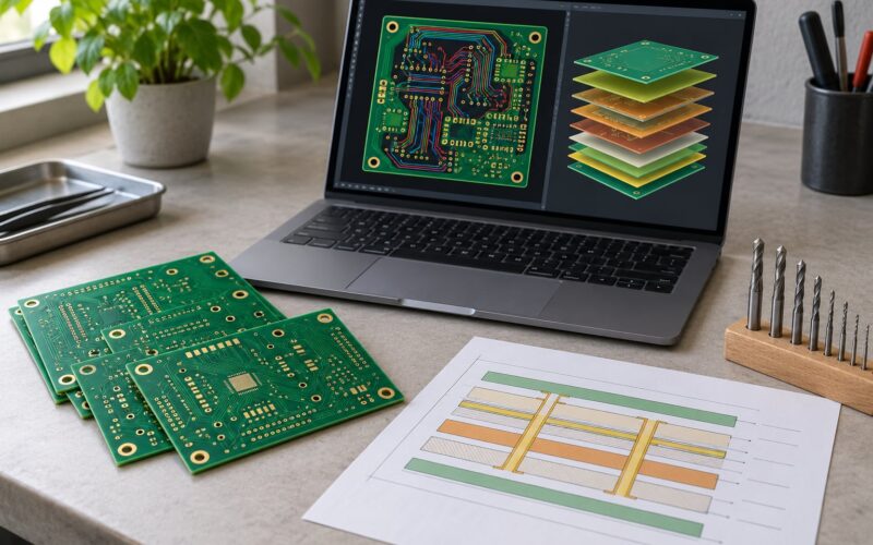
Solder mask is the epoxy coating that covers bare copper and opens up at the pads, while silkscreen is the ink legend printed on top of it to label parts. One protects the metal and controls where solder can go. The other tells the assembler what goes where. Soldermask and silkscreen explained, the split sounds simple, but the artwork behind the two layers behaves in very different ways, and mixing them up is one of the most common reasons a board comes back from a fab house with clipped legends or buried pads.
This guide walks through what each layer does, how each one is made, how they show up in your Gerber files, and the numbers that decide whether your board assembles cleanly. It is written for engineers who release Gerbers, plus anyone doing bench work, repair or debug on a board someone else designed.
Table of Contents
- What Is the Difference Between Soldermask and Silkscreen?
- Soldermask and Silkscreen Explained in One Table
- What Does Soldermask Do on a PCB?
- What solder mask defined and non-solder mask defined pads mean
- What happens without it
- What Does Silkscreen Do on a PCB?
- Courtyard is not silkscreen, and pick-and-place does not read it
- When to delete the legend entirely
- How Do Soldermask and Silkscreen Look in the Design Data?
- Soldermask and Silkscreen Explained in the Manufacturing Process
- Why your silkscreen gets clipped
- What Colors and Materials Are Available?
- What Are the Most Common Soldermask and Silkscreen Mistakes?
- How Do You Prepare Soldermask and Silkscreen Artwork?
- Soldermask and Silkscreen Design Rules for Readable Boards
- Frequently Asked Questions
- What is the main difference between soldermask and silkscreen?
- Is silkscreen the same as soldermask?
- Why is silkscreen usually white?
- Should silkscreen be placed over solder pads?
- Why is my silkscreen getting clipped by the solder mask?
- Can a PCB work without soldermask or silkscreen?
- Conclusion
What Is the Difference Between Soldermask and Silkscreen?
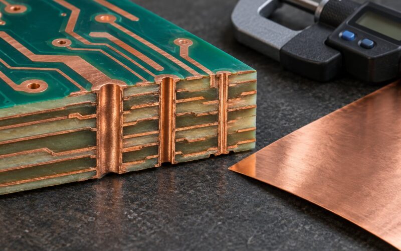
The difference is one of job and material. Solder mask, also called solder resist, is a structural coating in the board stack. Silkscreen, also called the legend or overlay layer, is a printed marking that sits on the surface of that coating and carries no electrical role at all.
Put physically: copper is the circuit, the mask seals and insulates it, and the silkscreen is paint on top of the paint. If you scraped the silkscreen off a finished board, the board would still work. If you scraped the mask off, you would have exposed copper, no solder confinement and a much shorter service life.
Soldermask and Silkscreen Explained in One Table
| Feature | Solder Mask | Silkscreen |
|---|---|---|
| Primary function | Protects copper from oxidation and corrosion, confines solder to pads | Identifies components, polarity, pin 1 and test points |
| Material | Liquid photoimageable epoxy (LPI) or dry film photoresist (DFSM) | Epoxy or polyester ink, sometimes UV-cured |
| Position in the stack | Directly on the copper and plated surface | On top of the cured solder mask |
| Electrical role | Insulating, though it sits close to copper and governs creepage | None, fully non-conductive and non-functional |
| Typical colour | Green, black, blue, red, white, matte variants | White most often, plus yellow, black and other light inks |
| Applied by | Screen coating plus UV exposure and developing, or dry film lamination | Screen printing, direct legend printing, or inkjet |
| Relationship to pads | Defines the pad openings; expansion and dam values matter | Must stay clear of pad openings or it gets clipped |
| Key design constraint | 3 to 5 mil expansion, 4 mil minimum dam | 40 mil text height, 5 to 6 mil line width, 4 to 6 mil pad clearance |
| Effect on assembly | Decides whether solder wets the pad or bridges | Decides whether an operator or AOI can read the board |
| Cost and yield impact | Adds a process step; defects here scrap boards | Cheaper, but adds review time and touch-ups |
What Does Soldermask Do on a PCB?
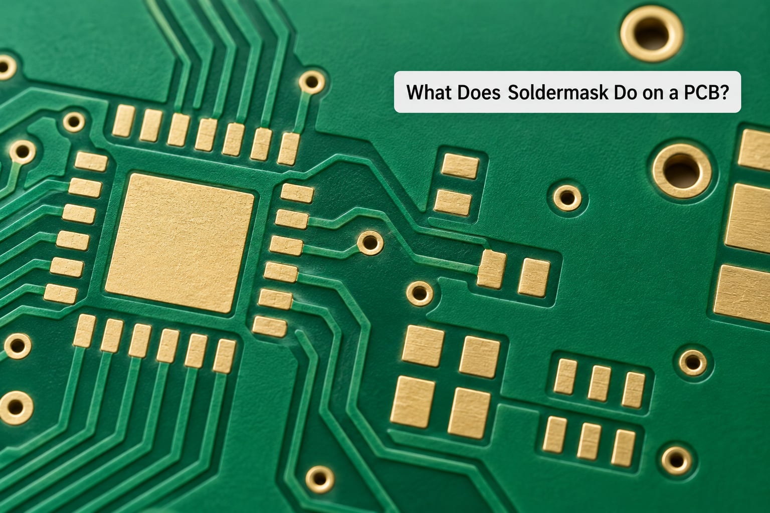
Four jobs, in order of importance. The mask keeps oxygen and moisture off the copper, so traces do not corrode between assembly and end of life. It defines where solder is allowed to sit, which is what stops a wave of molten solder bridging two adjacent pads. It adds a dielectric layer so a high-voltage design can hold wider trace spacing than bare FR-4 would allow. And it gives inspection a consistent background, so a defect in the copper shows up under AOI instead of hiding in a field of raw metal.
That second job is the one beginners underestimate. On a bare board, molten solder has nowhere to stop, so it wets along the trace and pulls toward its neighbour. With a mask opening sized slightly larger than the pad, the solder is confined, the fillet forms at the pad edge, and the joint looks the same every time.
What solder mask defined and non-solder mask defined pads mean
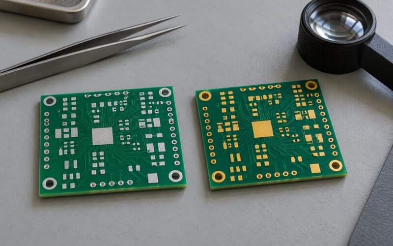
The pad style you choose changes what the mask does. In a solder mask defined (SMD) design, the copper pad is smaller than the mask opening, so the mask itself defines the solderable area. In a non-solder mask defined (NSMD) design, the mask opening matches the pad, so the copper defines the area.
NSMD is the default for fine-pitch work such as QFN and BGA footprints because it keeps more copper under each pad, which improves solder paste printing, thermal performance and tolerance to registration error. SMD pads still show up in libraries designed for older processes, and they remain useful where you want the mask edge to control the fillet.
What happens without it
A board can physically work with no mask. It is a bad idea. Hobbyists building their first board argue about this regularly, and the consensus in the Hacker News threads on the subject is that through-hole soldering without a mask is impractical: heat spreads along the exposed trace, the joint takes longer to make, and the board is left with copper that starts tarnishing as soon as it leaves the fab. For prototypes, bare copper plus a conformal coat is occasionally cheaper; for anything that ships, the mask earns its keep.
What Does Silkscreen Do on a PCB?
Silkscreen is information. It carries reference designators, polarity marks, pin 1 indicators, connector and switch labels, test point names, high-voltage warning symbols, board part numbers, revision codes and assembly notes. None of it conducts, and none of it changes how the board behaves electrically, which is exactly why it gets cut first when a designer is trying to save board area.
Cut it first, and then the assembly slows down. The reference designators are the most valuable thing on the layer, because they are the join between the board and the pick-and-place file, the bill of materials and the schematic. Reading them by eye is how a human finds TP4 during debug.
| Prefix | Component type |
|---|---|
| R | Resistor |
| C | Capacitor |
| L | Inductor |
| D | Diode, LED, or other polarity-marked device |
| Q | Transistor |
| U | Integrated circuit |
| J | Connector |
| F or FL | Fuse or filter |
| TP | Test point |
| + and minus | Polarity indicator for electrolytics and power inputs |
Courtyard is not silkscreen, and pick-and-place does not read it
Two persistent misconceptions come up in the KiCad and Altium communities, and both end with designers over-constraining their own boards.
The first is that courtyard and silkscreen are the same outline. They are not. Courtyard is a CAD-only construct used during design to check whether parts can sit side by side; it never reaches the fab house. Silkscreen is the only one of the two that is physically printed. The outline suggestions for both come from IPC-7351B/C and IPC-7352, which is why they look similar in a footprint library.
The second is the belief that pick-and-place machines read silkscreen to find parts. They do not. In a KiCad forum thread, experienced assembly engineers put it plainly: the machines place components from centroid coordinates in the pick-and-place file, and a board with silkscreen printed straight across the pads would assemble without complaint. The same thread notes that real machines vary widely in accuracy, so talking to your assembler beats trusting a universal number.
So do not shrink your whole layout to protect legend. Protect the reference designators, keep the pin 1 and polarity marks, and let the rest go where it needs to.
When to delete the legend entirely
Inside a dense BGA or QFN field there is physically no room for legible text, and trying to force it produces the thin slivers and clipped fragments that make a board look unfinished. The sensible rule is to drop silkscreen inside the footprint field, keep it outside where there is room, and add a separate assembly drawing if the assembler needs the detail.
How Do Soldermask and Silkscreen Look in the Design Data?
Both layers are positive-image Gerber files, and the polarity confusion around them is worth clearing up now. In the mask file, the drawn features are the openings: whatever you paint in the mask Gerber becomes a hole in the coating. In the silkscreen file, whatever you paint becomes ink. The mask file is often generated for you, from the copper layers plus an expansion value, but it can be drawn by hand when you need a partial mask or a custom opening.
| Design data element | Common layer name in CAD | Gerber extension | What it looks like |
|---|---|---|---|
| Top solder mask | Mask, Solder Mask Top, SMT Mask | .gts or .gbs | Solid shapes at every pad and via you want exposed |
| Bottom solder mask | Mask Bottom | .gbs or .gts | Same idea, mirrored to the bottom layer |
| Top silkscreen | Top Overlay, Legend, F.SilkS | .gto or .gbo | Text, outlines, arrows, logos, polarity marks |
| Bottom silkscreen | Bottom Overlay, B.SilkS | .gbo or .gto | Same content, mirrored |
| Mask openings control | Mask expansion, pad-to-mask setting | Not a file | A rule in the CAD tool that offsets each opening from its pad |
| Legend clipping | Silkscreen clip, keep-out from mask | Not a file | A DRC or CAM rule that trims legend off open pads |
| Assembly drawing | Drill drawing, fabrication drawing | .gbr, .txt | Board outline, drill table, notes, layer stack |
Extensions vary by CAM tool, so check your fab house’s list rather than assuming. What matters is that the mask and legend files are named and included separately, and that the stack note in your fabrication drawing says which colour the mask is.
Soldermask and Silkscreen Explained in the Manufacturing Process
Order matters here, because the legend is printed onto a surface that has to be fully cured. The typical liquid photoimageable (LPI) flow runs like this.
- Surface preparation. The bare board is cleaned, and the copper is micro-etched so the mask bonds to the surface rather than to a layer of contamination.
- Coating. Liquid mask is applied by curtain coating or screen printing and spreads across the panel, covering both copper and the substrate between traces.
- Pre-bake. A short bake removes solvent and leaves the coating tack dry, so it does not stick to the phototool during exposure.
- Exposure. UV light goes through a photomask, or the panel is exposed by direct imaging (DI). Exposed mask crosslinks and becomes insoluble.
- Developing. A developing solution washes away the unexposed coating, opening the pad windows. The board is rinsed and inspected under strong light, because residue here shows up later as failure to solder.
- Curing. A thermal or UV final cure hardens the mask so it survives reflow temperatures. The board is then routed and drilled.
Legacy work sometimes uses dry film solder mask (DFSM) instead, where a photoresist film is vacuum-laminated onto the panel and developed the same way. LPI is what nearly every fab house runs today, and the process sequence you should be designing against is the LPI one.
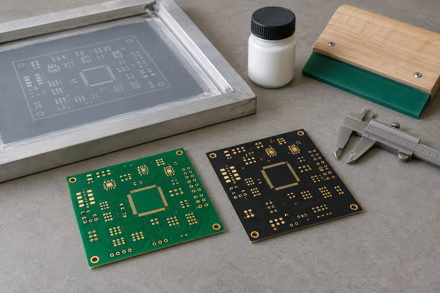
The silkscreen goes on afterwards. Traditional screen printing pushes ink through a mesh with a squeegee, one colour per screen, and the ink is then baked to harden. Direct legend printing (DLP) cures the ink with UV or laser as it is deposited, which removes the screens and suits short runs. Inkjet printing is the newest option, useful when you need many unique part numbers and no tooling.
Why your silkscreen gets clipped
Mask openings are cut before the legend is printed, and the fab house’s CAM step removes any ink that falls inside an opening. Left alone, silkscreen over an open pad would wick solder during reflow and could bridge a fine-pitch pad to its neighbour.
Four things cause clipping, and all four are fixable in your layout. Text crossing a pad or via gets trimmed mid-stroke. Legend drawn over a mask-defined keepout is cut back. Silkscreen running off the board edge is trimmed at the edge, which is why a border drawn 0.2 mm inside the profile loses its outside line. And silk text placed close to a copper trace can be flagged for poor legibility, a point that came up on r/PrintedCircuitBoard where a designer was told their fab publishes pad-to-silkscreen clearance but nothing about silkscreen-to-trace spacing.
The fix is the same in every case: add clearance in CAD, check it with your fab house’s DFM report before you pay for tooling, and do not rely on the CAM step to preserve something you drew too close.
What Colors and Materials Are Available?
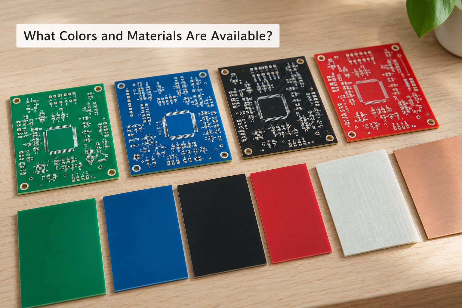
Green is the default because it is the easiest colour for AOI to see copper defects against, and it is the cheapest ink to make in volume. Blue, black, red, white and matte finishes are all normal production options now, and they cost a little more because the fabricator runs a different ink batch.
Silkscreen is usually white because white has the highest contrast against green, blue, black and red. On a black board, white is close to mandatory. On a red board, a white legend reads well, but a dark legend has better contrast, which is why red and white silkscreen combinations come with a contrast warning attached.
Two practical notes. White silkscreen on white soldermask is invisible, and yellow on light green is nearly as bad. And on a high-voltage board, the mask colour has no effect on creepage, but the mask coverage does, so keep the coating continuous between conductors rather than relying on a particular colour.
What Are the Most Common Soldermask and Silkscreen Mistakes?
Mask covering a pad. Too little expansion, or a manual mask edit drawn smaller than the pad, leaves no clean metal to wet. Solder beads, voids and a joint that never wets. A negative expansion of -0.05 mm on some pins is used deliberately by careful designers, but it has to be intentional, and a corrected TPS63070 footprint published on r/PrintedCircuitBoard did exactly that asymmetrically on the top pins.
Sliver or dam breakage. When two mask openings sit close together, the mask left between them is a sliver. Below about 4 mil it can break, and a broken sliver that curls up can lift a pad or bridge a gap. Widen the dam, or merge the openings into one.
Silkscreen over a pad. The classic version is a reference designator whose first character lands on a pad. The assembler gets a trimmed digit, or solder wicks into the ink and makes the joint non-wet. Keep 4 to 6 mil of clearance and let the CAD tool trim the rest automatically.
Residual mask or debris inside an opening. This is a process defect rather than a design one, but it shows up the same way, so check your DFM report for it and ask what the fab does about it.
Unreadable contrast. Light legend on light mask, or text so small it blurs at normal viewing distance, both come back to a minimum text height of about 40 mil, roughly 1.0 mm.
Legend drawn across a trace. The text is printed, but a nearby copper trace crossing behind it looks like part of the character, so the label reads as garbage. Move the silk or the trace.
Vias left exposed when they should be tented. An exposed via collects solder during wave or reflow and can wick it off a nearby pad, or bridge to a neighbouring net in a hand-soldered joint. Tenting a via, covering it with mask, trades away a little test access for a much lower defect rate.
A long-running SparkFun community thread covers the related argument of whether silkscreen should be drawn over the mask area or clipped to component outlines. The practical consensus is that readable legend beats a tidy mask, which is also why most fab houses default to clipping only at exposed metal.
How Do You Prepare Soldermask and Silkscreen Artwork?
Work through this before you zip the Gerbers. It takes ten minutes and saves a spin.
- Confirm both mask layers are present, top and bottom, even if you think you have no bottom parts.
- Check the mask expansion value against your fab house’s spec rather than the default your tool shipped with.
- Verify every pad has an opening, and every pad you meant to leave covered does not have one.
- Run DRC with the silkscreen-to-mask clearance rule enabled, so the tool clips legend away from every open pad. Do not turn that rule off.
- Check text height is at least 40 mil and line width at least 5 to 6 mil. Thicker than that if the board is large and viewed at a distance.
- Confirm polarity marks, plus and minus, pin 1 indicators and diode bars are all present and all readable.
- Look for silkscreen crossing the board profile, and pull it back from the edge.
- Leave room for the component body. Silk under a tall part is invisible, and silk under a moving part is a scrape risk.
- Name the files in your fab house’s expected convention, including the .gts or .gbs mask and .gto or .gbo legend files.
- Ask for a DFM or CAM review before the build, and read the mask and silk sections of the report. That is where clipping and dam issues show up while they are still cheap.
On the clearance conflict everyone runs into: different fab houses publish different numbers, and the forum threads about it are full of people comparing 0.15 mm, 0.26 mm and 4 to 6 mil. Treat your fab house’s published value as the one that matters and the values in this article as the industry floor. If your assembler runs the pick-and-place line, ask them directly, as one KiCad thread concluded, because machine accuracy varies and the person processing your job is the authority.
Soldermask and Silkscreen Design Rules for Readable Boards
Here are the numbers that decide whether a board assembles and reads cleanly. Use the mil value and the millimetre value together, since fab houses quote both and rounding is where mistakes happen.
| Design rule | Mil | Millimetres | Who sets it |
|---|---|---|---|
| Mask expansion per side | 3 to 5 | 0.08 to 0.13 | Fab house, applied to your copper data |
| Minimum mask dam between openings | 4 | 0.10 | Designer, and a hard limit on fine-pitch work |
| Minimum silkscreen text height | 40 | 1.0 | Designer |
| Minimum silkscreen line width | 5 to 6 | 0.13 to 0.15 | Designer |
| Silkscreen to solder mask clearance | 4 to 6 | 0.10 to 0.15, some fabs specify 0.26 | Fab house, enforced in CAM |
| Legend to board edge | 10 | 0.25 | Designer, and routing tolerance on top |
| Registration tolerance, mask to legend | Fab dependent | Fab dependent | Fab house capability |
A few habits that follow from those numbers. Keep the legend layer on a consistent grid so the whole board can be inspected quickly. Orient text so it reads when the board is held with the components up and the connector end nearest you, which is how it will be handled at test. Coordinate the mechanical and electrical data before release, not after, because the assembly drawing is what both the silkscreen and the mask are checked against.
And use IPC-2221 and the IPC-7351B/C family as the authority when a rule in your CAD tool disagrees with a rule you have read somewhere else. The fab house capability sheet wins over all of them, but the standards are what the capability sheet was written against.
Frequently Asked Questions
What is the main difference between soldermask and silkscreen?
Soldermask is a nonconductive coating applied over PCB copper to protect it from oxidation and to confine solder to pads, while silkscreen is a printed marking layer carrying component labels, polarity marks and other visual information. Soldermask defines the solderable surface and is part of the board structure. Silkscreen sits on top of it, conducts nothing, and only tells the assembler and the technician what is what.
Is silkscreen the same as soldermask?
No, though both are nonconductive PCB markings made in different ways. Soldermask covers and protects copper while leaving selected pads exposed, and it is applied before drilling and assembly. Silkscreen is printed onto the cured mask afterwards, carries reference designators and warnings, and is trimmed automatically anywhere it crosses a mask opening. Removing silkscreen leaves a working board; removing soldermask does not.
Why is silkscreen usually white?
White is the default because it gives the strongest contrast against green, blue, black and red soldermask, which is what assembly and inspection need to read. The required ink colour depends on your design and on what the fabricator’s process supports. White ink on a white mask is invisible, and a dark legend on a red board can read better, so contrast is worth checking before you commit to a colour pair.
Should silkscreen be placed over solder pads?
No, not as a rule. Silkscreen should stay clear of exposed pads, vias and any area that needs clean metal, because ink there can wick solder and stop a joint wetting properly. A small amount of overlap gets clipped by the fab house during CAM processing anyway, which leaves a truncated designator. Keep 4 to 6 mil, or 0.10 to 0.15 mm, of clearance and let the clipping rule catch the rest.
Why is my silkscreen getting clipped by the solder mask?
The fabricator’s CAM step removes any legend that falls inside a mask opening, because ink over exposed metal would wick solder during reflow. Clipping also happens at the board profile and at keepout areas. The causes are text crossing a pad, silk drawn over a keepout, silk running off the board edge, or text placed so close to a copper trace that it is flagged as garbled. Add clearance in CAD and check the DFM report before the build.
Can a PCB work without soldermask or silkscreen?
A board can work without either, and prototype services do offer bare copper, but you trade away real protection. Without soldermask, copper oxidises, solder wets along exposed traces, joints take longer to build, and a wave or hand solder operation bridges more often. Without silkscreen, assembly slows down and field debug gets slower because nobody can read the reference designators. Mask it; treat the legend as optional only on the cheapest prototypes.
Conclusion
Start by keeping the two artworks apart in your head and in your file list. Draw mask openings from the copper, expand them by your fab house’s value, and treat the silkscreen as a separate document that only has to stay clear of those openings. Then check both against the assembly drawing, confirm every reference designator, polarity mark and pin 1 indicator is readable at 40 mil or taller, and read the DFM report before you release the build. That sequence catches almost every mask and legend defect before it becomes a wasted spin.