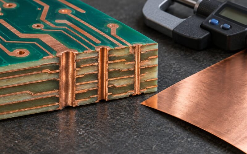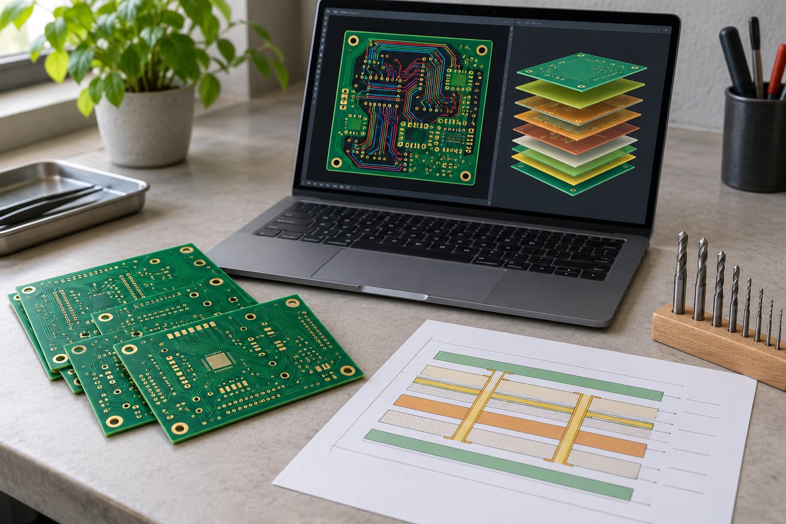
To prepare a PCB for fabrication, you finish the design, check it against your chosen board house’s real manufacturing limits, then export a verified package of Gerber files, an Excellon drill file, your stackup, and your fabrication drawing. If you also want parts placed, you add a bill of materials and a pick-and-place file on top of that. This guide covers how to prepare a PCB for fabrication step by step.
Here is the blunt truth about the process: manufacturing itself is highly automated and boring. Lamination, imaging, etching, drilling, plating, masking and routing are mature, repeatable steps any competent fab runs ten thousand times a year. The difficulty in building a PCB sits almost entirely in preparation.
That is where things go wrong. A missing copper layer, a drill file in the wrong format, a copper pour that swallows your isolation, an acid trap in an acute-angle trace — none of these produce an error message at your desk. They produce a rejected CAM review, a lead-time clock that restarts, and a board that arrives dead. Preparation is the one phase where a mistake costs you nothing but time.
The workflow below runs from requirements to submission in eight steps. It is written for the person who has a finished layout and now has to release it, whether that is a student’s first two-layer board or an engineering team’s EVT build. Last reviewed for 2026.
Table of Contents
- What You Need
- Step-by-Step: How to Prepare a PCB for Fabrication
- How to Prepare a PCB for Fabrication, in Plain Terms
- 1. Confirm the PCB Fabrication Requirements
- 2. Check the PCB Layout and Design Rules
- 3. Add or Verify Fabrication Data
- 4. Create and Inspect the Gerber Files
- 5. Create and Check the Drill Files
- 6. Add the Bill of Materials and Assembly References
- 7. Run a Final Preflight and Manufacturing Check
- 8. Package and Submit the Files
- Common Mistakes
- Frequently Asked Questions
- What files are needed for PCB fabrication?
- How do I make a Gerber file for a PCB?
- What is the difference between PCB and PCBA?
- What does a fabricator check in my design?
- How do I know if my design is manufacturable?
- How many prototype boards should I order on the first run?
- Conclusion
What You Need
You cannot check a package you never assembled. Before you start, gather these six things.
The design source files. The schematic and board database in whatever ECAD tool you use, saved and versioned. The fab never sees these, but you need them to regenerate outputs whenever something changes.
Your fabricator’s capability data. This is the single most underrated item. Every serious board house publishes a minimum feature table: minimum trace and space, minimum hole, minimum annular ring, aspect ratio, copper weight, surface finish, tolerance on finished holes. Generic DRC rule sets in ECAD tools assume a high-end process. A low-cost fab’s real limits are looser, and designing to the wrong rule set is how you get a rejection.
Layer stack and board profile. How many layers, what laminate, what finished thickness, what copper weight on each layer, and the board outline. For any board with a defined impedance, you also need a stackup and impedance targets.
The output job files. Your ECAD tool’s fabrication output configuration, saved as a reusable job. Setting up units, leading-zero format, layer naming, and file extensions once and reusing it across revisions prevents a whole class of silent errors.
Assembly reference data, if you want a PCBA. Component part numbers, manufacturer names, a pick-and-place source, and assembly drawings showing orientation. Where approved parts exist, note them.
A Gerber viewer. A free one is fine. What matters is that you can toggle layers, measure features and view the board in 3D before a single file leaves your machine.
Step-by-Step: How to Prepare a PCB for Fabrication
How to Prepare a PCB for Fabrication, in Plain Terms
A board is fabrication-ready when the manufacturer can build it without asking you a question. Concretely, that means every layer exists as its own file, the holes match the layers, the written specifications state anything the artwork cannot express, and the package says which revision it is.
Three deliverables do the heavy lifting. The Gerber files are the per-layer manufacturing artwork — each copper layer, the solder mask, the silkscreen, and if you need one, the paste layer. The Excellon drill file is the numerical control program describing every hole and slot, including which are plated. The fabrication drawing is a document a CAM engineer reads alongside the artwork for anything geometry cannot carry: surface finish, tolerances, impedance targets, special instructions.
Everything else — BOM, pick-and-place, assembly drawings — belongs to assembly, not fabrication. Keeping those two packages mentally separate removes the most common ordering mistake.
Here is the file map that falls out of that split.
| File | Extension | Purpose | Who consumes it |
|---|---|---|---|
| Copper layer artwork | .GTL, .GBL, .G1, .G2 | Etched conductive pattern for each layer | Fab |
| Solder mask | .GTS, .GBS | Where resist is removed to expose pads | Fab |
| Silkscreen (legend) | .GTO, .GBO | White component outlines, polarity marks, text | Fab |
| Outer copper / inner copper set | .G1 through .G30 | Every conductive layer, named by number | Fab |
| NC drill program | .TXT, .DRL, .XLR | Every hole and slot, tool by tool, plated or not | Fab |
| Drill drawing / table | .DRR, .DRT | Human-readable list of hole sizes and tolerances | Fab |
| Electrical netlist | .IPC, .LNT | IPC-356 netlist used for bare-board electrical test | Fab |
| Fabrication drawing and notes | Dimensions, stackup, finish, tolerances, instructions | Fab | |
| Board outline / profile | .GKO, .GML | Routing path and edge definition | Fab |
| Stackup definition | .PDF or tool export | Layer-by-layer materials, thickness, copper weight | Fab |
| Bill of materials | .CSV, .XLSX | Part numbers and quantities to buy | Assembler |
| Pick-and-place (centroid) | .CSV, .CPL, .TXT | Component X, Y, rotation, and side | Assembler |
| Assembly drawings | Top and bottom component placement views | Assembler | |
| Paste / stencil layer | .GTP, .GBP | Apertures defining solder paste deposit per pad | Assembler |
| Gerber job file | .GBRJOB | Machine-readable layer stack and file mapping | Fab and assembler |
1. Confirm the PCB Fabrication Requirements
Before touching the layout, write down what you are actually ordering. Board dimensions and outline, layer count, base material, copper weight, surface finish, minimum trace and space you will actually use, minimum hole, hole tolerance, and solder mask and silkscreen colors.
These are not formality. They are the difference between a quote that arrives in a day and a quote that comes back full of questions. Every parameter you leave undefined is a parameter the CAM engineer assumes on your behalf, and their assumption may not match your design intent.
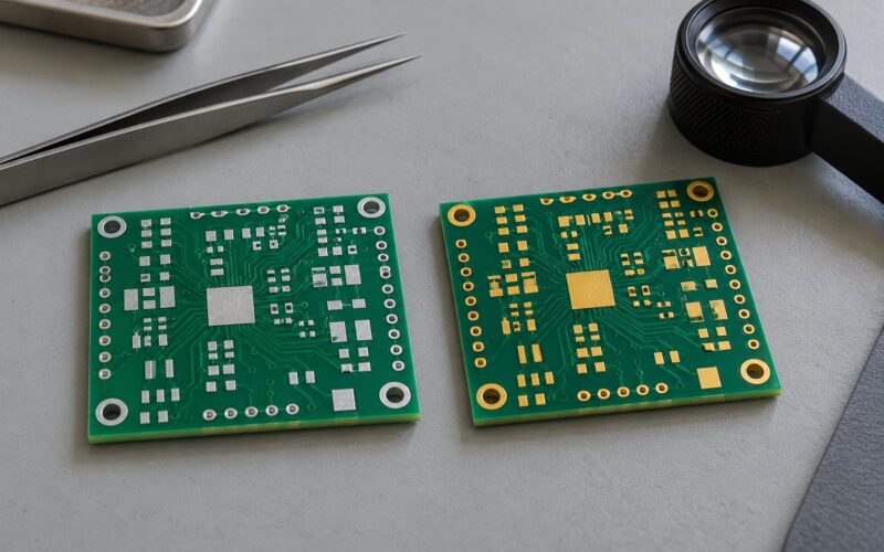
Decide the surface finish early. For hand-soldered prototypes, lead-free HASL is forgiving and cheap. For fine-pitch parts, or anywhere you need flat pads, ENIG is the usual choice. Immersion gold and immersion tin are options when a specific requirement demands them.
If any signal on the board has a defined impedance, say so in writing with target values and tolerances. A fab will not guess your stackup, and an unstated impedance target means no impedance control at all.
2. Check the PCB Layout and Design Rules
Now check the layout against the fabricator’s published limits, not your tool’s defaults. Load the board house’s rule set into your DRC if one is offered. If not, set the constraint values manually to match the published table.
While the DRC runs, look at the things a rule engine will never catch. Trace widths that are legal but unmanufacturable at a specific corner. Vias placed where the next layer’s plane would be destroyed. Copper pours touching copper traces on the same net and different nets alike. Pads placed on the board edge with no mask dam. Components spaced so tightly that the pick head cannot approach them.
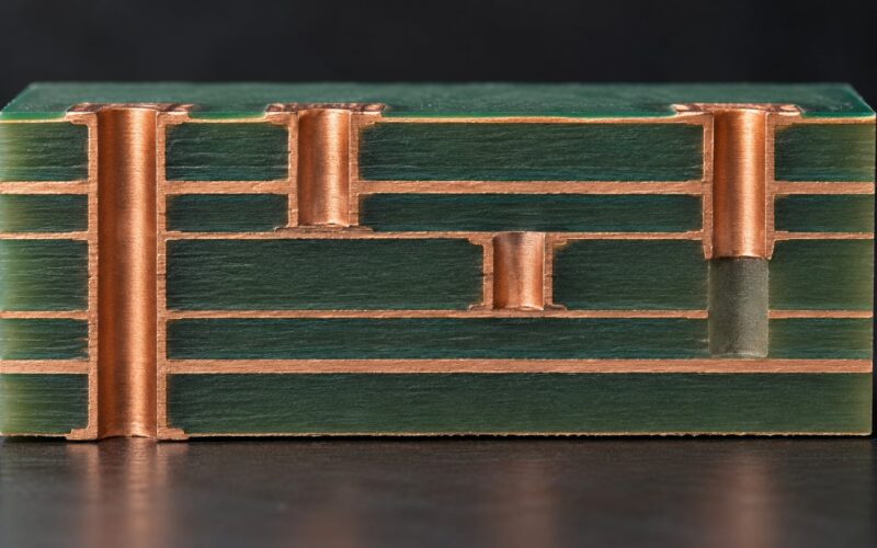
Check the mechanical side too. Every hole needs its annular ring intact, so keep copper clear around it. Plated holes should be annular in the artwork, not added as a separate copper shape later. Mounting holes need a stated size, a stated plating status, and enough clearance that a screw head cannot touch a nearby trace.
Here is what typical capability classes look like. These are realistic ranges for commercial board houses, not a specific vendor’s guaranteed specification — always confirm against your chosen fab.
| Feature | Advanced process | Standard process | Low-cost process |
|---|---|---|---|
| Minimum trace / space | 3 mil / 3 mil | 5 mil / 5 mil | 6 mil / 6 mil |
| Minimum finished hole | 8 mil | 10 mil | 12 mil |
| Minimum annular ring | 5 mil | 7 mil | 8 mil |
| Maximum aspect ratio (plated) | 12:1 | 10:1 | 8:1 |
| Hole tolerance (plated) | +/- 0.001 in | +/- 0.002 in | +/- 0.003 in |
| Layer count (typical max) | 24 and above | 12 to 16 | 4 to 6 |
If a clearance on your board falls below the class you are ordering, either change the design now or change the process class. Both are fine. What is not fine is finding out at CAM review.
3. Add or Verify Fabrication Data
The artwork cannot express intent, so the documentation carries it. Your fabrication drawing needs the board dimensions and tolerances, the layer count and which layer is which, the stackup, the surface finish, the solder mask and silkscreen colors, hole tolerance, any impedance targets, and a revision number.
Write notes for the things that are genuinely ambiguous. Routing direction on a controlled-impedance layer. Copper weight on inner planes. Whether a set of holes is plated or not. Where a specific component must sit, and how close it must sit to the board edge. Which side the fiducials are on.
A worked note reads something like this: 4-layer FR-4, 1.6 mm finished thickness, 1 oz outer and 0.5 oz inner copper, ENIG finish, green solder mask, white legend. 50 ohm single-ended controlled impedance to +/- 10 percent, referenced to the stackup on sheet 2. All 0.3 mm plated holes per drill table; four 3.2 mm mounting holes unplated, 5.0 mm copper keepout. Break tabs on the panel edges are not permitted.
That paragraph alone prevents several rounds of clarification email.
4. Create and Inspect the Gerber Files
Export Gerbers from the CAM or output job. Set units to millimeters unless your fab specifies otherwise, use 4:5 or 4:6 leading-zero format, enable block apertures, and keep one file per layer. Do not merge layers, and do not let the export flatten your copper pours into a single region without connectivity.
Always ship the Gerber job file that your tool generates alongside the artwork. It tells the CAM system which file is which layer, and a machine that guesses the stackup order from filenames is a machine that will eventually guess wrong.
Once exported, open the package in a viewer and check it layer by layer. This is the highest-value habit in the whole workflow, and the one most first-time senders skip.
Load each layer alone and confirm the expected content. Copper layers should show pads, traces and poured regions. The mask layer should show openings at pads only. The silkscreen should show outlines, reference designators, polarity marks, and pin-1 indicators. The outline should be a closed shape with no gaps.
Then look for the classic export failures: a missing internal layer, a silkscreen swapped with the mask, copper pour fills that swallowed nearby traces, polarity that disappeared, text converted to outlines in the wrong layer, and board dimensions that do not match your drawing.
Use the viewer’s 3D mode last. It is a crude way to catch missing components and shifted footprints, and it takes a minute.
5. Create and Check the Drill Files
Drill data is a separate export and the most commonly mishandled deliverable. Two things must be right: the format and the plating status.
Generate the NC drill program in Excellon format. Set the units to match your Gerbers, confirm the zero suppression format matches too, and confirm whether the tool expects leading or trailing zeros. A mismatch here is one of the most common reasons a package is rejected, because the drill coordinates are silently read as the wrong values.
Verify the plating status. A plated through hole is a hole whose barrel is copper-plated; a non-plated hole is a bare laminate hole, used for tooling, mounting, or alignment. The drill file, the copper artwork, and the drill table all have to agree. A mounting hole plated when you meant it unplated costs money and time.
Check the drill report. Every tool should have a diameter, a plating flag, a count, and a tolerance class. Compare total hole count against the number of footprints with holes. If two tools overlap within a drill bit diameter of each other, split them into a slot or move one; overlapping hits can break bits mid-board and produce burrs or breakout.
Finally, compare the drill holes against the copper layers. A plated hole should be surrounded by an intact annular ring on every layer it passes through. A hole sitting on a plane without its own pad leaves a void in that plane that will show up as a return-path discontinuity on high-speed nets.
6. Add the Bill of Materials and Assembly References
Be precise about what these are for. The BOM (bill of materials) and the pick-and-place file do not tell the fabricator how to make a bare board; they tell an assembler what to place and where. If you are ordering bare boards, they are optional. If you are ordering a PCBA (a populated board), they are the entire assembly handoff.
For the BOM, use manufacturer part numbers rather than generic descriptions wherever possible, because a part number resolves to one exact component. Include quantity, reference designators, manufacturer, and any approved alternates. Flag the parts that are genuinely hard to source.
The pick-and-place file is the centroid data: for each component, its X and Y position, its rotation, and which side it sits on. Keep the coordinate origin documented, because an assembly house using a different origin will place the entire board backwards. Note that in the assembly drawing, not just in a filename.
Add assembly drawings showing the top and bottom with the designator visible on every part, and mark polarity clearly: the plus on an electrolytic, the pin-1 triangle, the diode bar, the orientation of every one-way part. A silkscreen mark that vanishes under a new footprint is a defect, so verify markings against the footprint you are actually shipping.
Finally, think about test points. A small number of labelled pads on key nets costs almost nothing and saves a probe during bring-up. Decide now, not after your first board is assembled and unmeasurable.
7. Run a Final Preflight and Manufacturing Check
Run your EDA tool’s own preflight or output-job checker, then do the checks it cannot do.
Visually, inspect the assembly render one more time at full size, checking part placement and rotation. Electrically, run the design rule check with the fabricator’s values, and confirm zero errors and that you understand every warning. For connectivity, run an electrical rule check on the schematic and confirm the netlist exported from the schematic matches the layout’s net count.
For files, confirm the layer set is complete, the drill file matches the copper artwork, the outline is closed, the Gerber job file is present, and every file in the package is the current revision. A single leftover file from the previous revision is a genuinely common cause of a wrong board.
For documentation, confirm the drawing states the same revision, the same dimensions, and the same finish as the artwork. Then check the panelization decision: for a first run, most builders order single boards or a shared panel with breakaway tabs. If you panelize, verify the design rules account for the tab routings, that the fab does not mistake a tab for a defect, and that fiducials sit where a machine can see them on every board in the panel.
Finally, name every file identically, with the revision and a short project descriptor, and archive the entire output set before you transmit it. When the fab asks for a change in four days, you will want the exact package you sent, not a regenerated one.
8. Package and Submit the Files
Assemble one folder or one archive containing every file with a consistent naming scheme. Send it as a single download rather than a folder tree, so nothing gets lost in transit.
State the revision and the order intent plainly: bare boards or assembled, quantity, target layer count, surface finish, and the build stage if you have one (EVT for engineering validation, DVT for design validation, PVT for production validation). A fabricator who does not know which stage you are at will assume your smallest run and your most relaxed tolerances.
Then read the confirmation. A CAM engineer will either accept the package or return a DFM report listing each flagged item. That report is normal on a professional release, not a sign of failure. Expect it to mention things like isolated copper, unconnected pads, text too small to read, or a design rule outside the process window.
Triage it: for each flag, decide whether to fix the design, adjust the requested process class, or accept the risk in writing. Fix the design for anything that affects function. Accept in writing for anything cosmetic. Then resubmit as a new revision and keep the original archived.
Before payment, confirm the returned stackup matches what you specified, especially on impedance-controlled boards, and confirm the finished thickness, copper weight, and surface finish are written on the order. A quote that quietly drops to a different laminate is worth catching here rather than on the box that arrives.
Common Mistakes
These are the errors that show up repeatedly in CAM review, and each one is cheap to prevent.
Shipping a default DRC rule set. Your tool assumes a capable process. A low-cost fab’s real minimum feature is looser, so a board that passes cleanly in your tool can still be rejected. Load the fabricator’s numbers, or set them by hand.
Leaving copper pours in an undefined state. Whether a pour is hatched, filled, or left as a polygon changes the etch result and the connectivity. State it in the output job and in the notes, and confirm in the viewer that nearby clearances survived the fill.
Acid traps in acute-angle traces. A sharp inner corner in a trace can hold etching chemistry that no rinse removes, leaving a notch that may or may not break the conductor. Round or chamfer those corners. This is a visual check in the viewer, not a rule the DRC knows about.
Overlapping drill hits. Two holes close enough to share a bit position can cause breakout, burrs, or a broken bit inside the board. Move them apart or convert the pair into a routed slot.
Missing solder mask dams. When two mask openings nearly touch, the exposed gap fills with solder and the pads bridge. Widen the mask opening gap, or reduce the opening size, so a real dam of mask survives between them.
Confusing the fab package with the assembly package. Ordering a PCBA and sending only Gerbers leaves the assembler unable to place anything. Ordering bare boards and expecting parts is a different, more common mistake. Decide which you want before you upload.
Version drift. Quoting rev A and sending rev B, or regenerating outputs after the design changed without updating the revision label, produces boards nobody can trace. One naming convention applied to every file solves it.
Silkscreen that disappears. Overlapping reference designators, text under a component body, or a polarity mark that falls outside a new footprint all vanish at print. Silkscreen is printed before assembly, and a mark hidden under a body is a mark nobody can read during bring-up.
One habit prevents most of these: open the finished package in a viewer, at real scale, and look at every layer on its own. It takes ten minutes, and it catches the majority of what would otherwise cost a week of lead time.
Frequently Asked Questions
What files are needed for PCB fabrication?
For bare boards you need the copper layer Gerbers, the solder mask and silkscreen layers, the board outline, the Excellon NC drill program, the drill drawing, and a fabrication drawing with your notes. Add the Gerber job file and, for any board with defined impedance, the stackup. An IPC-356 netlist lets the fab run bare-board electrical test. Bill of materials, pick-and-place, and assembly drawings are only needed if you are ordering a populated board.
How do I make a Gerber file for a PCB?
In your ECAD tool, open the CAM or output job configuration, select Gerber format, set units and leading-zero format, and export one file per layer including mask, silkscreen, and outline. In KiCad the path is File, Plot, then Generate Drill Files; in Altium it is Project, Outputs, Fabrication Outputs. Always keep the generated Gerber job file, and never merge layers. Open the result in a Gerber viewer before sending it anywhere.
What is the difference between PCB and PCBA?
A PCB is the bare printed circuit board: laminate, copper, drilled holes, solder mask, and silkscreen. A PCBA is that board after components have been placed and soldered onto it. Fabrication consumes Gerbers, drill data, and a fab drawing. Assembly adds a bill of materials, a pick-and-place file, assembly drawings, and sometimes a paste layer. Ordering the wrong one is the most common first-time mistake.
What does a fabricator check in my design?
A CAM engineer checks the file set for completeness, then the artwork for manufacturability: minimum trace and space against their process, hole sizes and annular rings, aspect ratio, copper-to-copper and copper-to-edge clearances, and whether your notes match the geometry. Many runs also come back with a DFM report listing isolated copper, unconnected pads, or text too small to print. Review it item by item before approving production.
How do I know if my design is manufacturable?
Set your design rule constraints to the published capability of the specific board house you intend to use, not to your tool’s defaults, and run DRC with those values. Then look for what rule checking misses: acid traps in sharp trace corners, overlapping drill hits, missing solder mask dams, copper pours merging nets, and component spacing a pick head cannot reach. Confirm the final answer visually in a Gerber viewer, and ask your fabricator to run a DFM check before you commit to a run.
How many prototype boards should I order on the first run?
Five is the most common first-run quantity because it gives you spares for two or three soldering mistakes while keeping the cost low. If your board is large, consider ordering several small designs together on a shared panel, which lowers the per-board cost but adds breakaway tab work. For anything with fine-pitch parts or tight impedance targets, buy a few more than you think you need, because the next board is usually a revision.
Conclusion
Start with the fabricator’s capability table, not your layout. Load their minimum feature numbers into your design rules, then export, open the package in a Gerber viewer, and look at every layer on its own before you transmit anything.
That is how to prepare a PCB for fabrication in a way that leaves nothing to guesswork. Everything else in this guide is detail on that one idea: the more completely you specify the board, the fewer decisions a CAM engineer has to make on your behalf. Preparation is where mistakes are free. After the order is placed, they are not.