Gerber files explained for PCB manufacturing comes down to one idea: a Gerber file is a flat, per-layer picture of your board that a fabricator turns into real copper, mask, legend and holes. This guide walks through what sits inside a fabrication package, which file answers which question, and the checks worth running before you send anything to a shop.
Table of Contents
- What Are Gerber Files in PCB Manufacturing?
- Gerber Files Explained for PCB Manufacturing
- What Is the Difference Between Gerber Files, Drill Files, and CAD Files?
- Which Gerber Layers Are Required for PCB Manufacturing?
- How Do Apertures, Pads, and Tracks Work in a Gerber File?
- How Do You Check Gerber Files Before Sending Them to a Manufacturer?
- What Common Gerber File Errors Cause PCB Manufacturing Problems?
- How Should Gerber Files Be Named and Packaged for a PCB Order?
- Frequently Asked Questions
- Are Gerber files safe to send to a PCB manufacturer?
- Do I need to send drill files separately from Gerber files?
- What is the difference between Gerber X2 and standard Gerber?
- Why does my PCB drill file not line up with the copper layers?
- What should a manufacturer check in a Gerber file before quoting my PCB?
- Can a fabricator repair missing connectivity in Gerber files?
- Conclusion
What Are Gerber Files in PCB Manufacturing?
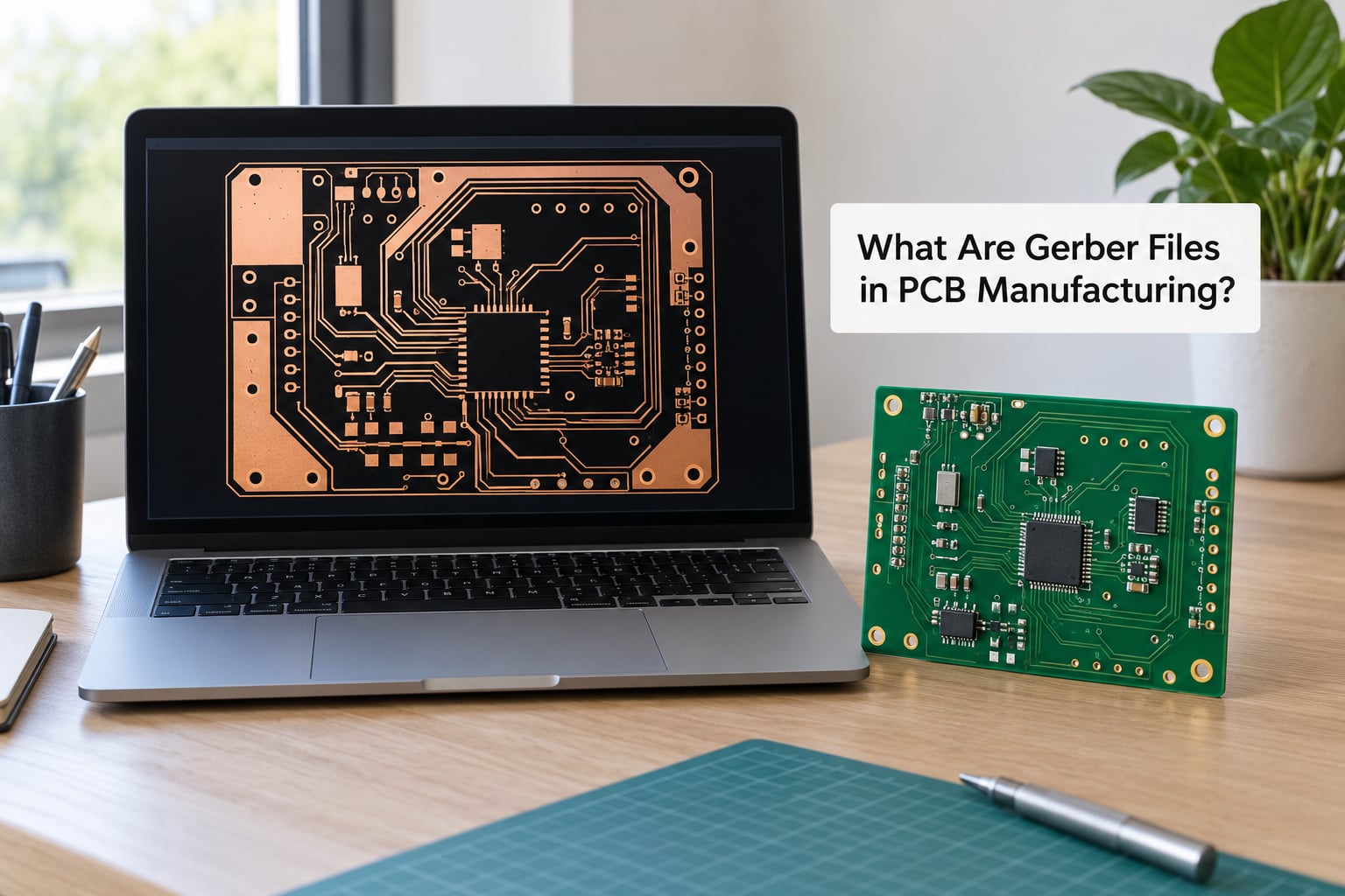
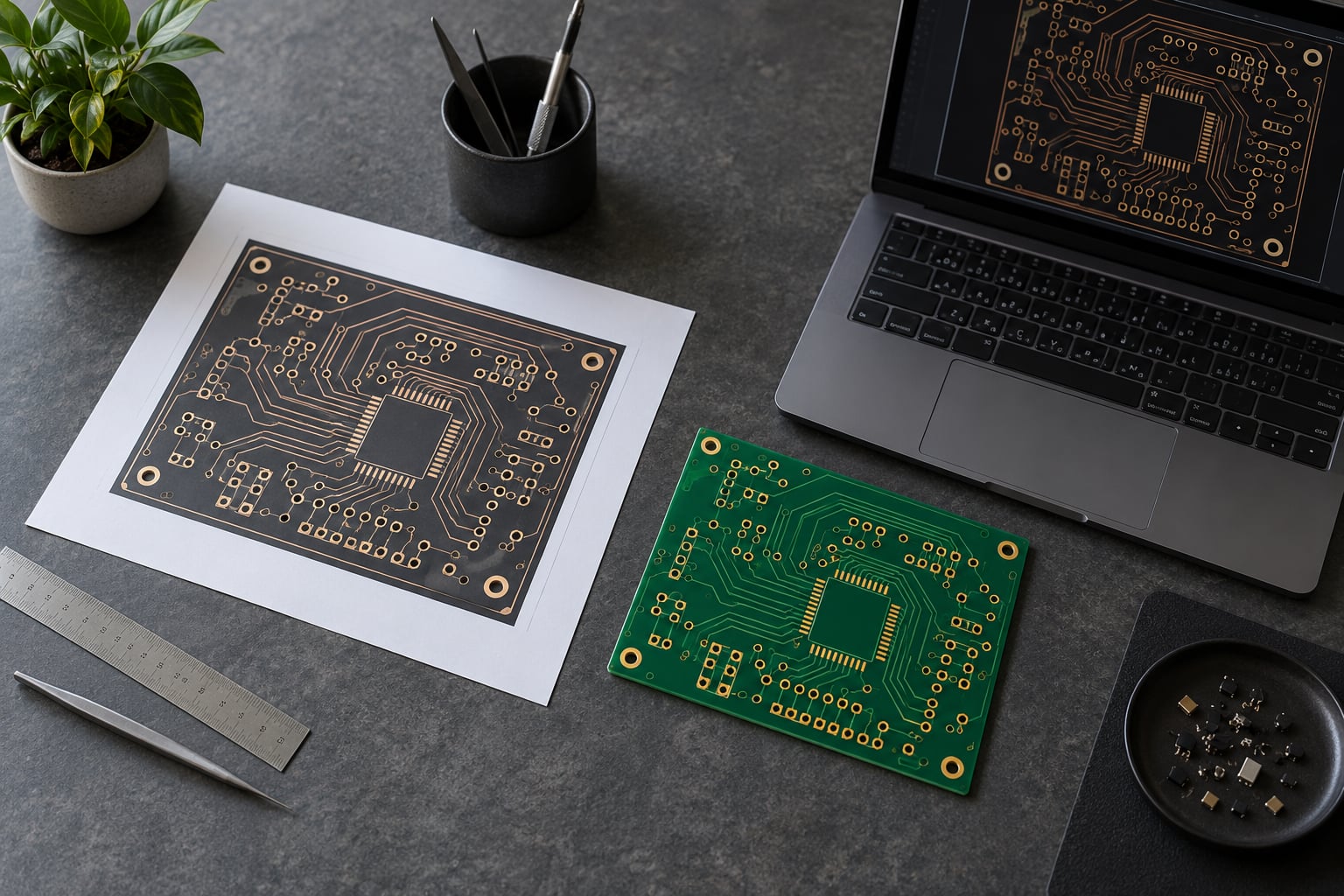
A Gerber file is a 2D vector fabrication artwork file: a plain-text “light drawing” of one printed circuit board layer, written in the RS-274X specification that every major PCB CAD tool exports. It carries the exact geometry of that layer — trace widths, pad shapes, clearances, mask openings, reference designators, board edge — and nothing more.
It is not your design. A Gerber is a flattened picture of your design: connectivity is gone, component names are gone, and the file has no sense of which pad belongs to which net. That is the whole point. It is a manufacturing output, not an editable source.
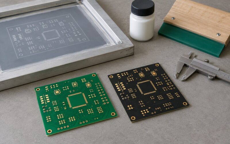
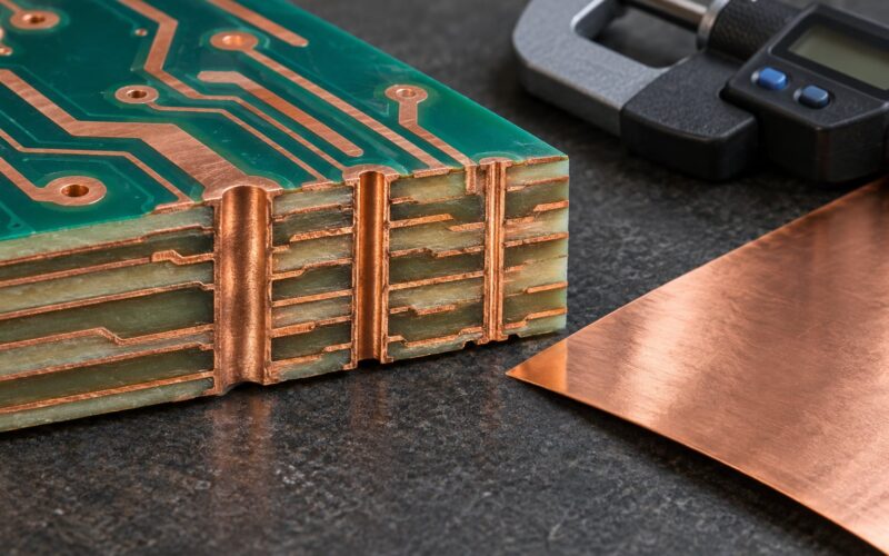
When a package reaches a fabricator, a CAM engineer imports the layer set, checks it against the factory’s own process window, and generates the phototools and drill program from it. From there the data drives physical steps: imaging copper, pressing the layers together in a laminate stack, etching away the unwanted copper, printing solder mask and legend, drilling and plating holes, then routing the boards out of the panel. The Gerber package is the complete description of the board geometry, so anything missing from it cannot be recovered downstream.
Gerber Files Explained for PCB Manufacturing
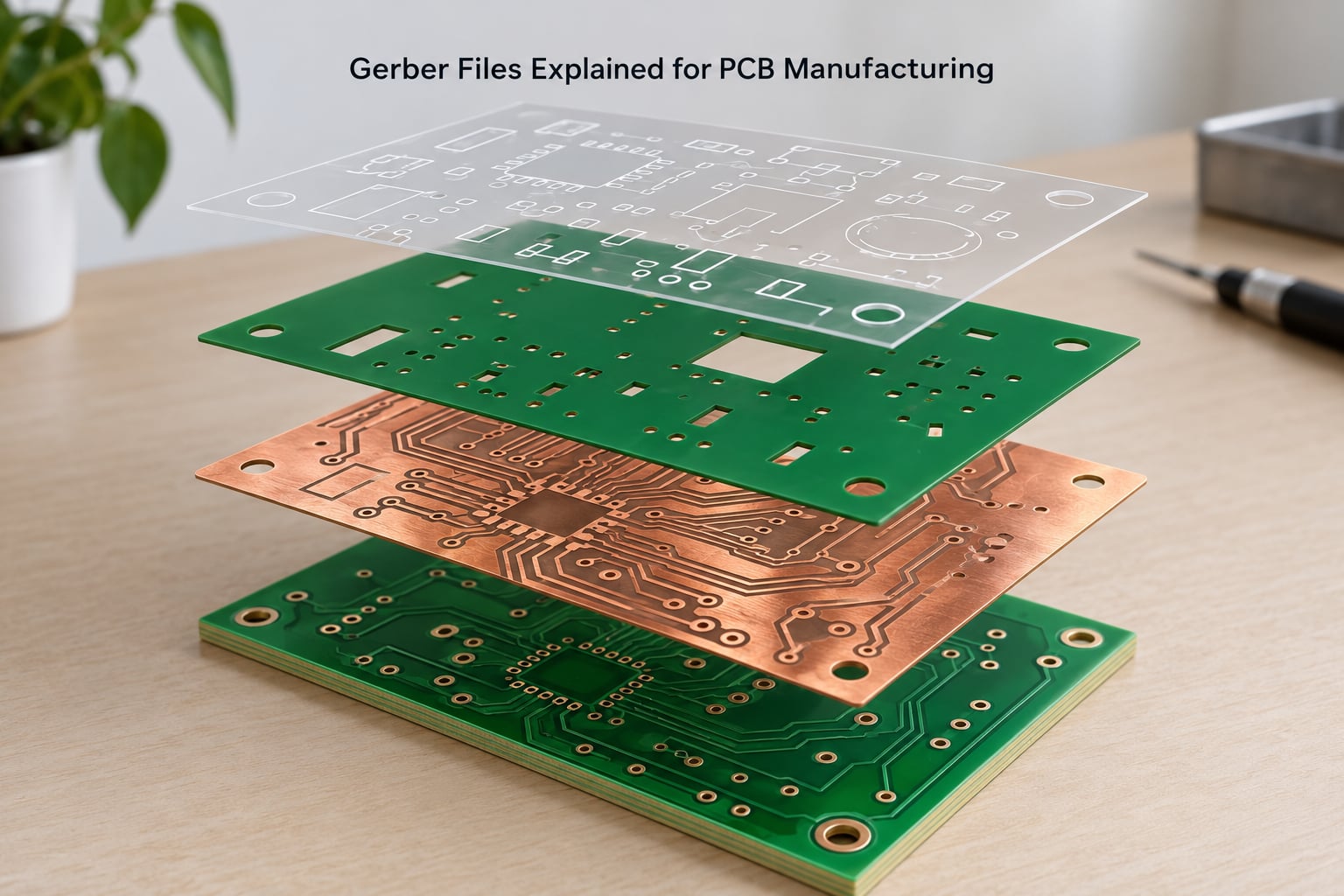
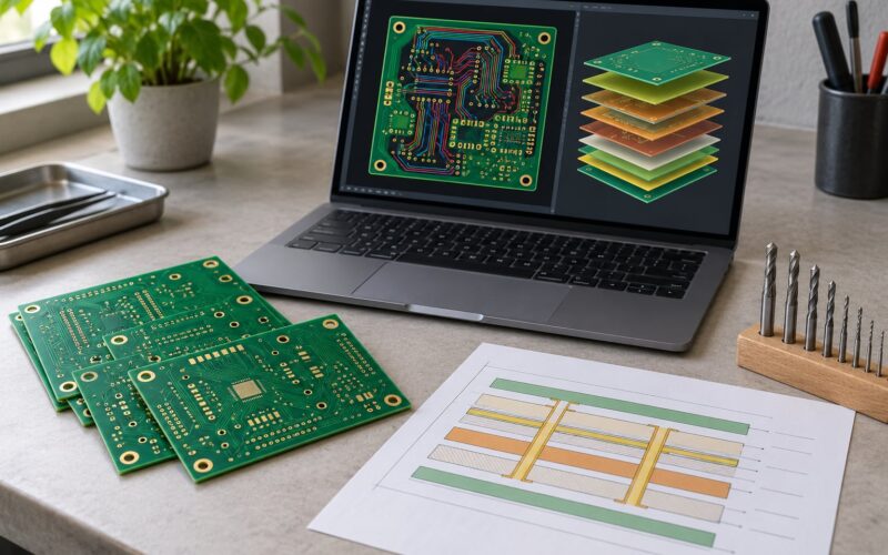
One board needs several Gerber files, because a Gerber file only ever describes a single layer. A two-layer board usually produces four or five; an eight-layer board with a ground plane on every inner layer produces considerably more.
Every layer file follows the same internal structure. It opens with a header that declares the format (FS, MO, AD, G04 comments), then defines apertures — the reusable shapes the image is drawn with. A circular pad might be aperture 11, a 0.25 mm track aperture 21. After the definitions come the drawing commands, which move the image head and either draw, move, or flash each aperture at specific coordinates.
Here is what that vocabulary maps to on a real board:
| Layer file | Typical extension | What it controls |
|---|---|---|
| Top copper | .GTL | Topside traces, pads, pours and plane connections |
| Bottom copper | .GBL | Bottom-side copper artwork |
| Inner copper | .G1, .G2, .G3 | Signal and plane layers inside the stackup |
| Top solder mask | .GTS | Openings that expose pads; the green coat everywhere else |
| Bottom solder mask | .GBS | Bottom-side mask openings |
| Top silkscreen | .GTO | White reference designators, polarity marks, outlines |
| Bottom silkscreen | .GBO | Bottom-side legend |
| Top paste | .GTP | Apertures for the solder paste stencil, assembly only |
| Bottom paste | .GBP | Bottom-side stencil apertures |
| Board outline | .GKO, .GM1 | Routing path, slots and cut-outs |
| Drill data | .TXT, .DRL | Hole coordinates and tool sizes (Excellon) |
The extensions are conventions, not requirements. A fabricator’s CAM tool identifies layers by content and by the X2 attributes if they are present, so renaming a file usually breaks nothing technically. It does, however, make the CAM engineer guess, and guessing is where orders get held for clarification. Keep the standard names.
What Is the Difference Between Gerber Files, Drill Files, and CAD Files?
Gerber files describe surfaces. Drill files describe holes. CAD files describe intent. Conflating them is the single most common source of confusion for people new to the handoff, so it is worth being precise about which file answers which question.
| File type | Format | Carries | Connectivity? |
|---|---|---|---|
| Gerber layer artwork | RS-274X, X2, X3 | Geometry of one layer: traces, pads, mask, legend, outline | No |
| NC drill file | Excellon | Hole coordinates, tool diameters, plating flags, slot routing | No |
| IPC-356 netlist | IPC-D-356A | Net assignments for electrical test after build | Yes, one-way |
| CAD source | KiCad project, Altium file, OrCAD, Eagle | Full editable board: layers, netlist, components, rules | Yes |
| ODB++ | ODB++ | Layer artwork plus panel, netlist and assembly data in one structure | Yes |
| IPC-2581 | IPC-2581 | Full manufacturing description: layers, netlist, BOM, assembly, test | Yes |
So, is a Gerber file a CAD file? No. It is a derived, flattened, single-purpose output of a CAD file. The distinction matters in practice: if a pad needs to move after export, the Gerber cannot be edited meaningfully. You change the design and re-export.
Drill data is the exception that proves the rule. Because holes are physical voids rather than deposited artwork, they live in a separate Excellon file with its own coordinate system. Practitioners describe the result bluntly: gerber files do not include drill holes, which is why a package missing the drill file produces a board with every pad intact and no way to mount a component. When a board arrives with holes that miss the pads, the usual cause is a drill file exported from a different origin or datum than the copper layers, and the two sets of coordinates no longer agree.
Extended Gerber formats add metadata without adding layers. X2 attaches structured attributes to apertures and objects, so a file can declare itself as a solder mask or a profile. X3 adds assembly attributes such as component part and function data to X2. Both remain backwards compatible with RS-274X readers, which is why asking for “X2 files” is a safe default on a modern package.
Which Gerber Layers Are Required for PCB Manufacturing?
For a bare board, the required set is small and the rest is assembly data. Copper for every layer in the stackup, solder mask and silkscreen on both sides, a board outline that closes, and a drill file that matches those layers. Paste layers are only needed if you want stencilled boards. Paste mask files are needed for assembly, not fabrication.
Knowing which layer drives which physical step makes it far easier to spot a missing file, because each step needs exactly one piece of artwork:
| Gerber layer | Physical fabrication step it drives |
|---|---|
| Inner copper (image layers) | Laminating the prepreg and core into a stack, then imaging for the inner etch |
| Top and bottom copper | Imaging the outer layers and etching back to leave traces, pads and planes |
| Solder mask | Applying the solder resist coat and its pad openings |
| Silkscreen | Printing the white legend layer |
| Drill file | Drilling, plating and the mechanical aspect of vias and pads |
| Board outline | Routing or scoring the finished board out of the panel |
| Paste | Laser-cutting the solder paste stencil used during assembly |
Now the part that catches experienced engineers out. A Gerber package does not carry stackup, dielectric thickness, impedance targets, laminate material, copper weight or surface finish. Those live in the fabrication drawing and the specification notes, and they are not optional decoration.
Engineers posting on the eevblog forums have made the point that layer separation on a four-layer prototype can vary from about 0.1 mm to 0.25 mm depending on the fabricator’s published stackup, and that number changes the trace width you need for a given impedance target. An online calculator run against assumed dimensions will be approximate at best. Reading the actual stackup for the shop that will build the board is the difference between a controlled impedance design and a guess that costs money and returns boards that fail signal integrity testing.
How Do Apertures, Pads, and Tracks Work in a Gerber File?
Reading a Gerber file means reading three things: the aperture definitions, the coordinate data, and the drawing commands that connect them. Everything else in the file is comment.
An aperture definition block looks like this in a typical RS-274X file:
%ADD10C,0.600*%
%ADD11C,1.600*%
%ADD21C,0.250*%
Read it as: aperture 10 is a circle 0.600 mm across, aperture 11 is a circle 1.600 mm across, and aperture 21 is a circle 0.250 mm across. The C is the aperture shape code, and the number is the diameter in whatever measurement the file declared in its header. Circles, rectangles, obrounds and polygons all get defined this way, and they are the only shapes that can appear on the layer.
The drawing commands then place and move them:
%ADD11C,1.600*%
D11*
X1000000Y2000000D03*
X2000000Y2000000D01*
D03 flashes aperture 11 at the first coordinate. D01 draws a line to the second coordinate using the current aperture, which produces a 1.6 mm wide track between them. D02 moves without drawing. Those three codes, plus D10 for switching the active aperture, cover most of what happens in a real copper file.
That coordinate format looks odd because of how it is encoded. The MO command declares the measurement system, and the FS command declares the coordinate format. With the common FS44X44 setting, the last digit before the X or Y is an implicit decimal point and the leading digits are the whole number, so X1000000 reads as 100.0000 in the file’s declared measurement. This is the source of the well-known advice to export at 4:4 coordinate precision or higher. Two extra digits of precision sound trivial, and on a 0.1 mm grid they are not.
Pads, tracks, vias and flashes are all just these operations. A via is two flashed annular rings, one on each copper layer, joined by a plated hole from the drill file. A pad is a flash. A track is a D01 draw. A copper pour is a large filled region defined by the aperture and boundary coordinates. Polarity matters too: dark objects add copper, clear objects remove it, which is how a pour is knocked out around a trace.
How Do You Check Gerber Files Before Sending Them to a Manufacturer?
Every CAM package worth having will open and render your layer set, and any competent fabricator will review it before production. Doing the same check yourself takes about ten minutes and catches the failures that cause delays: incomplete or mistitled packages, mismatched drill alignment, and geometry that falls outside the shop’s process window.
Follow this sequence:
- Open the package in a Gerber viewer. Most tools have one built in, and standalone viewers exist for KiCad, Altium, EasyEDA and DipTrace output. Load every file in the zip, not just the copper.
- Confirm the layer count. Compare what rendered against what your stackup says it should be. A six-layer board missing both inner planes usually means an unselected layer in the export dialog, not a CAD bug.
- Check drill alignment. Overlay the drill file on each copper layer. Holes should sit dead centre in their pads with a visible annular ring all round. This is the fastest way to catch an origin mismatch.
- Verify the outline is closed. The routing path must form one complete loop. An open outline leaves the shop unable to determine the final board dimensions, and that question alone will hold the order.
- Look at clearances and widths. Zoom into the tightest gap on the tightest net. Many fabricators quote against a minimum trace and space, commonly around 0.1 mm, and anything tighter is flagged or refused.
- Check polarity on the mask layers. Mask files should be positive: drawn areas are openings, not mask coverage. Inverted mask artwork is one of those errors that looks plausible on screen and produces an unusable board.
- Read your file names against the contents. If the file called bottom silkscreen renders copper-coloured artwork, stop and re-export.
- State the design rules you used. A short fabrication note listing your stackup, copper weight, finish and any impedance targets gives the CAM engineer something to check against instead of guessing.
The CAM engineer’s role is worth understanding, because it sets expectations. The convention in the industry, repeated by practitioners on r/PCB, is flag but do not fix: a CAM engineer will tell you that a clearance sits outside the shop’s process window, but will not quietly correct your design for you. That boundary protects you from building a board that does not match what you intended.
Export settings are worth getting right once. In Altium, an OutJob file saves the whole output configuration — layer set, format, precision, drill options — so you stop re-walking the export menu every revision. KiCad, EasyEDA and DipTrace all have equivalent saved output job profiles, and reusing one is the cheapest way to eliminate a whole class of recurring export errors.
What Common Gerber File Errors Cause PCB Manufacturing Problems?
Almost every delayed PCB order traces back to a data problem rather than a design problem. The errors below cover most of what comes through.
| Error | What it causes | Fix |
|---|---|---|
| Missing layer (mask, silkscreen, outline or drill) | Order held for clarification, or a board built without a finish layer | Count rendered layers against your stackup and re-export the missing file |
| Drill file exported from a different origin than the copper layers | Holes miss the pads; the board cannot be assembled | Export drill data and copper from the same job configuration, then overlay them in a viewer |
| Board outline absent or unclosed | Final board size unknown; routing delayed | Include a routing path layer and confirm it forms one closed loop |
| Inverted polarity on a mask file | Mask covers the pads instead of opening them | Review mask layers in the viewer and re-export as positive |
| Trace or clearance below the fabricator’s minimum | DFM rejection or a design change after quote | Check the shop’s published capability table before ordering |
| Ambiguous or non-standard file names | CAM engineer has to request clarification; build queue slips | Use the standard extensions with a project and revision prefix |
| Stackup and impedance notes missing | Boards built to a generic stackup, impedance targets missed | Add a fabrication drawing or notes page listing stackup, material and finish |
One more deserves mention because it is easy to hit: exporting before every component is placed and every courtyard is settled. Component side assignments drive both silkscreen and paste files, so a board exported mid-layout arrives with legend and stencil data that do not match the assembled result.
How Should Gerber Files Be Named and Packaged for a PCB Order?
A well-named package removes an entire category of back-and-forth. The convention that works is a project prefix, a revision identifier, and the standard layer extension.
acme-sensor-v2/
  acme-sensor-v2.gtl
  acme-sensor-v2.gbl
  acme-sensor-v2.gts
  acme-sensor-v2.gbs
  acme-sensor-v2.gto
  acme-sensor-v2.gbo
  acme-sensor-v2.gko
  acme-sensor-v2.drl
  acme-sensor-v2.gbrjob
  README.txt
Keep the board outline named as a routing path rather than an ambiguous mechanical layer. A .gbrjob file is the Gerber job manifest Gerber X2 uses to state which file is which layer, and most fabricators prefer it when it is present. Put the drill file in the same directory, not a separate one.
The README is where the things Gerbers cannot carry belong: board thickness, copper weight, surface finish, solder mask and legend colours, stackup with dielectric thicknesses, any impedance targets with their tolerances, panelisation and tooling-hole details, and the minimum feature sizes your design assumes. Keep assembly files separate unless the fabricator is also doing assembly — BOM and pick-and-place belong in their own folder so nobody confuses them with fabrication data.
On revision control, one practical habit stands out from the community: when a design changes between revisions, diff the two Gerber sets rather than trusting your memory of what moved. Layer-by-layer comparison in a viewer, or a script that compares the two zips file by file, catches accidental edits to copper pours and silkscreen that nobody made on purpose. For open-hardware projects, people have had language models read two Gerber revisions and report the differences, which works well as a second pair of eyes on a large file.
If a set contains more than one distinct board design rather than one design repeated on a panel, say so in the README. Fabricators apply different handling rules to multiple designs in a single package versus a single design stepped out across a panel, and knowing which you sent avoids a delay at the quoting stage.
Frequently Asked Questions
Are Gerber files safe to send to a PCB manufacturer?
Yes. A Gerber package is plain text describing only geometry, with no credentials, executable code or confidential design history beyond the artwork itself. Manufacturers expect them by email, upload portal or zip attachment every day. The one thing to check before sending is your IP situation: if the design is not yet public, confirm the fabricator’s NDA terms before uploading to an online quoting service, because many of them store your files on shared infrastructure.
Do I need to send drill files separately from Gerber files?
Yes. Drill data lives in its own file, usually Excellon format with a .TXT or .DRL extension, because holes are physical voids rather than deposited artwork. Most exporters write it for you alongside the Gerber layers. Send it in the same directory as the copper layers and export it from the same job configuration, since a mismatch in origin between the two sets is the usual reason drilled holes miss their pads.
What is the difference between Gerber X2 and standard Gerber?
Standard Gerber is RS-274X, which describes geometry only: apertures, coordinates and drawing commands. Gerber X2 keeps exactly the same geometry but adds structured metadata attributes, so a file can declare itself as a solder mask or a profile layer without relying on its filename. X3 builds on X2 by adding assembly data such as component part and function attributes. Both remain readable by RS-274X tools, so X2 is a safe default.
Why does my PCB drill file not line up with the copper layers?
Almost always an origin or datum mismatch. The drill file and the copper layers were exported with different reference points, so the coordinates describe different physical locations and every hole sits off its pad. Export both from a single saved output job rather than configuring them separately, then load both into a Gerber viewer and overlay them. Holes centred inside their pads with a clear annular ring confirm the match.
What should a manufacturer check in a Gerber file before quoting my PCB?
A CAM engineer checks layer completeness against the stackup, that the drill file aligns with the copper layers, that the board outline forms a closed loop, that traces and clearances meet the shop’s process window, and that the stated material and copper weight are achievable. Any issue is flagged back to you. The convention is flag but do not fix: the engineer reports a problem, you correct the design and re-export.
Can a fabricator repair missing connectivity in Gerber files?
No, and the reason is worth understanding. Gerber files describe geometry only, with no netlist, so there is nothing in the artwork saying which pad connects to which. If connectivity is missing, it means a copper layer is absent, not that the fabricator can infer it. To add netlist data you need a different format: IPC-356 provides net assignments for electrical test, while ODB++ and IPC-2581 carry full netlist, assembly and BOM data alongside the artwork.
Conclusion
Start with the export. Generate the full fabrication output from one saved output job, including the drill file and the routing path, and include a fabrication note covering stackup, material, copper weight and finish. Then open the whole package in a Gerber viewer, overlay the drills on the copper, and confirm the outline closes before anything leaves your machine. When the package arrives, ask the fabricator to confirm what they see before release to production. That single question catches most of what would otherwise become a week of email.