Differential pair routing explained in one line: you run two copper traces side by side, keep their length and spacing matched, and let the receiver read only the voltage difference between them. Everything else in this guide follows from that idea — trace geometry, skew limits, via symmetry, reference plane continuity, and the handful of layout mistakes that break a link which should have worked. If you are new to high-speed layout, read straight through; if you are refreshing for a multi-Gbps interface, jump to the controls table and the workflow at the end.
Key takeaways
- A differential pair is two coupled traces carrying equal-magnitude, opposite-polarity signals; the receiver subtracts one from the other and throws away whatever arrived equally on both.
- Length mismatch between the two traces (intra-pair skew) closes your eye diagram. Budget skew as a fraction of the unit interval, typically 1 to 2 percent for most interfaces.
- Differential impedance is set by trace width, edge-to-edge gap, dielectric height, and the dielectric constant of your actual stackup — not by the width of either trace alone.
- Keep the pair coupled, parallel, evenly spaced, and over one continuous reference plane. Minimum vias, placed symmetrically with a ground via alongside.
- Never length-match by meandering one trace. Add length in coupled sections only, so both traces keep the same delay per millimetre.
- Verify before you fabricate: field-solver impedance numbers, length report, DRC with the diff-pair rules on, then TDR or an eye diagram on the first article.
Table of Contents
- What Is Differential Pair Routing and Why Does Symmetry Matter?
- Differential Pair Routing Explained: What Controls Performance?
- Differential Pair Routing Explained by Geometric Symmetry
- How Much Differential Pair Length Matching Is Required?
- How Do Trace Width and Spacing Determine Differential Impedance?
- How Should Vias, Layer Changes, and Stubs Be Handled?
- Why Do Continuous Reference Planes Matter?
- When Is Differential Routing Preferable to Single-Ended Routing?
- What Workflow Produces a Reliable Differential Pair?
- Frequently Asked Questions
- Should both traces in a differential pair have exactly the same length?
- Can a differential pair cross a split power or ground plane?
- Should differential trace width and spacing remain constant around obstacles?
- How can skew be measured after a PCB is fabricated?
- Is a short via stub harmless in a low-speed differential connection?
- Conclusion
What Is Differential Pair Routing and Why Does Symmetry Matter?
Differential pair routing is the practice of laying out two copper traces on a PCB so they run side by side with matched length and constant spacing, carrying equal-magnitude, opposite-polarity signals that a receiver reads as a single logic level. Differential pair routing explained properly starts with one fact: the receiver cares about voltage difference, not voltage.
One trace carries the data stream, usually named D+ or P. The other carries the exact inverse, D- or N. The differential line receiver amplifies the difference between them and discards the average, which is the common-mode voltage. Any noise that couples equally onto both traces — a switching current on a neighbouring net, a radiated field from an adjacent clock, ground bounce picked up by both conductors — appears at the receiver as common mode and cancels.
That cancellation is why symmetry is not a stylistic preference. The cancellation only works if both traces see the same surroundings: the same width, the same gap, the same dielectric beneath them, the same reference plane, the same number of vias, and roughly the same length. Break any one of those and the two signals no longer arrive with matched delay and matched attenuation, so part of the noise stops cancelling and the difference signal degrades.
Differential signaling also radiates far less than single-ended routing, because the opposing currents produce opposing magnetic fields that largely cancel outside the pair. It tolerates ground offset between two boards where a single-ended signal would simply see a shifted logic level. Those two properties, noise immunity and low EMI, are the real reasons multi-Gbps interfaces like USB, PCIe, HDMI, Ethernet, and MIPI all settled on this architecture.
The trade is cost. Two traces take twice the copper, they constrain where components can sit, they need matched vias at every layer change, and they need a controlled-impedance stackup that a board house can actually hold to. A differential pair is the right tool for a fast link across a noisy board, and pure overhead on a slow link.
Differential Pair Routing Explained: What Controls Performance?
Six things decide whether a differential pair works: length match, trace geometry, physical symmetry, differential impedance, the reference plane underneath it, and the transitions at vias and connectors. The rest of this article takes them one at a time.
| Control | Why it changes the signal | Typical target |
|---|---|---|
| Length match | Difference in propagation delay becomes intra-pair skew, which closes the receiver eye | 1 to 2 percent of the unit interval for most links |
| Trace width and gap | Sets differential impedance and decides how much field stays between the two traces | Set by the interface standard, calculated on your stackup |
| Physical symmetry | Identical geometry keeps delay and attenuation equal on both conductors | Same layer, same width, same gap, same length |
| Reference plane | Defines the return path and the characteristic impedance of each trace | Continuous, unbroken, directly underneath |
| Via and connector transitions | Add inductance, anti-pads, and discontinuity that shift impedance locally | Paired vias, same spacing at both ends, ground via alongside |
| Pair-to-pair spacing | Reduces differential-mode crosstalk from the neighbouring pair | 5W to 10W edge-to-edge for aggressive links, 3W as a floor |
Differential Pair Routing Explained by Geometric Symmetry
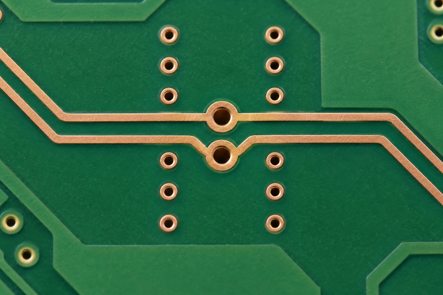
Symmetry is geometric before it is electrical. Two traces of identical width, separated by a constant gap, running parallel over the same dielectric and referencing the same plane propagate at the same velocity and lose the same energy to copper and dielectric loss along the route. Every one of those equalities is a condition the receiver depends on.
Change any of them and the two conductors stop being interchangeable. Widen one trace by a few thousandths of a millimetre and its delay per millimetre changes. Route one trace over a slightly thinner dielectric section and its impedance changes. Give one trace an extra via and its propagation delay grows by the length of that via barrel plus the anti-pad clearance, which on a fast edge is a measurable slice of the budget.
The practical version of the rule is simple: when a differential pair has to move around something, both traces move around it by the same route. Practitioners describe routing one trace of a pair around an obstacle while the other takes a shortcut as the most common pair-breaking mistake on a board, because the two traces then have different delay and different crosstalk environments along the whole detour.
How Much Differential Pair Length Matching Is Required?
Length matching exists to control intra-pair skew, the difference in arrival time between the two traces of a pair. When the traces are different lengths, the two halves of the symbol no longer line up at the receiver, and the vertical eye opening shrinks by roughly the skew. Push skew far enough and one bit latches as two or misses entirely.
The useful way to set a budget is to start from the edge rate, not the clock. The slowest meaningful frequency component of a digital signal is usually taken as roughly 0.35 divided by the rise time, and on FR-4 the propagation delay is around 150 ps per millimetre, or about 6.2 inches per nanosecond. A 1 Gbps link with a 1 ns unit interval that must hold skew under 20 ps therefore needs the two traces within about 0.13 mm of each other, and most designers set the constraint tighter than the spec to leave margin.
Typical published allowances follow the interface rather than the rate. USB 2.0 is commonly budgeted around 0.1 ns, roughly 15 mm on FR-4. PCIe guidance is often quoted near 1 mm on a short link. LVDS display links and MIPI CSI-2 are tighter still, in the tens of picoseconds, because their edge rates are far higher.
For most PCB work the number that matters is the one in your interface specification, and your constraint should be a fraction of it. Match to the spec and you have no margin for vias, connectors, and stackup tolerance; match to half of it and you do. On boards where skew is not critical, tolerance of a few millimetres is fine — the rule of thumb is that skew matters once the edge rate makes the horizontal opening of the eye smaller than the mismatch.
How Do Trace Width and Spacing Determine Differential Impedance?
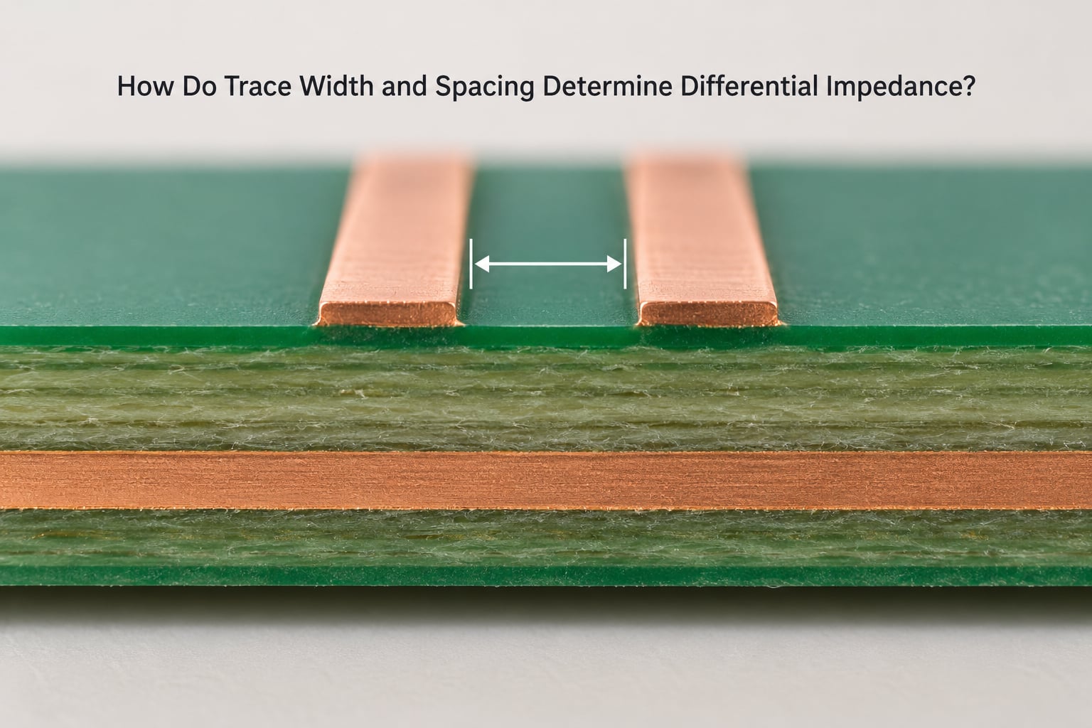
Differential impedance is not the impedance of either trace. It is what the receiver sees looking across the two conductors, and it depends on the pair as a coupled structure: the width of each trace, the edge-to-edge gap between them, the distance to the reference plane, and the dielectric constant of the material involved. The approximate relationship for a coupled pair over a plane is Z_diff = 2 × Z0 × (1 − 0.347 × exp(−2.9 × S / H)), where Z0 is the single-ended impedance of one trace in that geometry, S is the gap between traces, and H is the height to the reference plane.
Read that as a trend rather than a production number. Increase the gap and the coupling between the traces drops, so the differential impedance climbs toward twice the single-ended value. Narrow both traces together at a fixed ratio and the impedance rises for the same reason. Widen a trace and the impedance falls. The gap term is weak at large S/H ratios and strong at small ones, which is why on a thick dielectric the gap matters less than the width, while on a thin one the gap dominates.
| Layout style | Reference plane | Routing constraint | Notes |
|---|---|---|---|
| Coupled microstrip | Solid plane on the adjacent layer | Pair edge-to-edge gap is the impedance control knob | Fastest and easiest to inspect, but radiates a little more |
| Coupled stripline | Planes above and below | Both height and gap must be held | Better shielding, slower, needs more via stubs managed |
| Edge-coupled (asymmetric) | One plane | Gap on both sides kept equal where the tool allows | The usual choice; simplest to fabricate and tune |
| Broadside-coupled | Planes above and below | Traces stack vertically rather than side by side | Stronger coupling and common-mode rejection, harder to route and inspect |
Two numbers worth memorising because they come up in every interface: USB is designed around 90 ohm differential, and PCIe, HDMI, DisplayPort, 100Base-T Ethernet, LVDS under TIA/EIA-644, and MIPI CSI-2 and DSI are designed around 100 ohm. CAN and RS-485 in their usual bus forms run at other values again, typically around 60 ohm and 120 ohm respectively, so read the transceiver data sheet rather than assuming.
Here is the part that trips people up. Impedance is a function of the whole stackup, not of the copper. Board houses quote a target impedance against a specific stackup with a stated tolerance, commonly plus or minus ten percent, and the copper weight, solder mask, and prepreg all shift the number. So do not copy a width and gap from a blog, including this one. Build the stackup first, run the geometry through a field solver such as the one built into your EDA tool or the Saturn PCB Toolkit, and give the board house your target impedance with the stackup attached.
One more geometry note: the tightest legal spacing is a trade-off, not a rule. Coupling and common-mode rejection improve as the gap closes, but crosstalk from the adjacent pair worsens and fabricators have a minimum spacing limit based on their process. Most designers pick the smallest gap that hits the impedance target and their fabricator’s minimum, then use extra space between pairs rather than inside them.
How Should Vias, Layer Changes, and Stubs Be Handled?
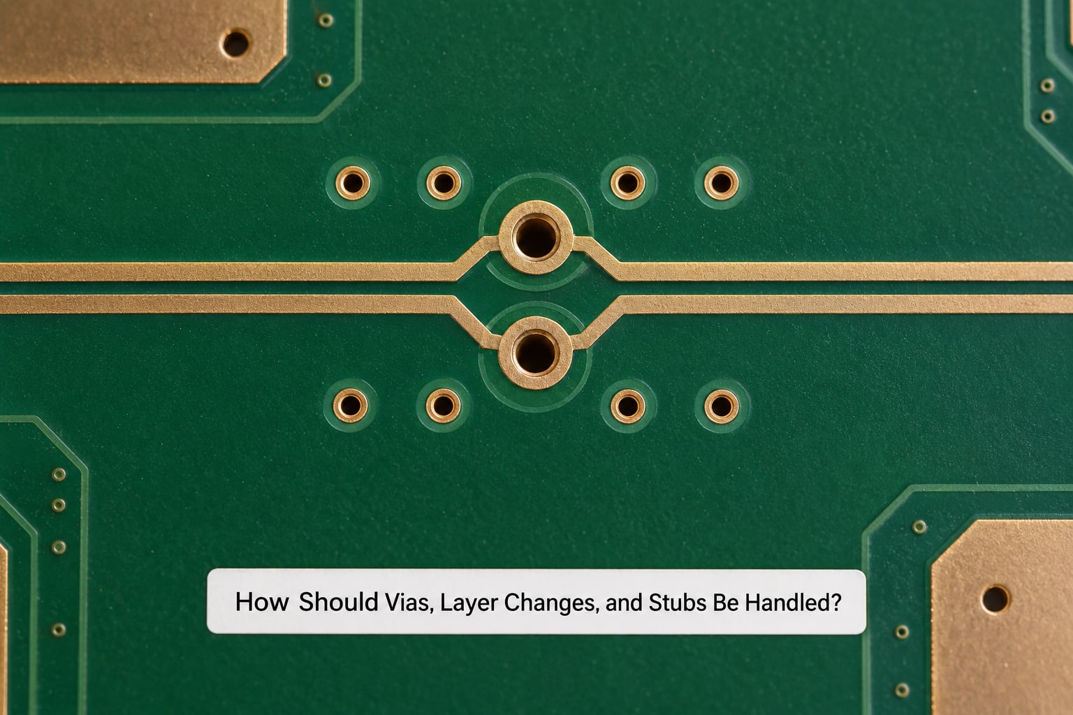
A layer change is the weakest point on most differential pairs, because a via barrel and its anti-pad replace a perfectly uniform coupled structure with a discontinuity. The job is to make that discontinuity identical on both conductors and as short as possible.
- Use two vias, one per trace, with the same diameter and the same antipad clearance. A single fat via for the pair is not equivalent; each conductor needs its own return path.
- Keep the via spacing identical at the driver and at the receiver. Practitioners report the symmetric fanout at both ends as what produces the best result, and it is the cheapest fix when the ends look different.
- Place a ground via alongside each transition. This stitches the reference planes so the return current has a low-inductance path straight through the layer change instead of detouring.
- Keep the pair coupled into and out of the via field. Fan out symmetrically, then become a coupled pair again as soon as the geometry allows.
- Avoid unused branch stubs. A stub left on either trace, or a via that goes nowhere, is a small antenna that reflects energy back at the edge rate. At multi-Gbps rates this shows up as a visible bump on the eye diagram.
The same logic applies at a connector. If the connector’s pin assignment puts the two signals on non-adjacent pins, fan them symmetrically to a coupled route and add ground vias at the breakout. If they are adjacent, keep the escape short and straight.
Why Do Continuous Reference Planes Matter?
A high-speed trace is not really a wire carrying current to the far end. It is one half of a circuit: signal on the trace, return current on the plane beneath it. The impedance the receiver sees only exists because of that return path.
When the plane under a pair is continuous, the return current flows straight back along the mirror image of the signal and the fields stay confined between them. When the plane splits — a plane split under a regulator, an analog and digital partition, a gap between pour regions — the return current has to detour around the gap. That detour turns a small loop into a large one, and large loops radiate and pick up noise. A pair crossing a void on an inner layer is the same problem in a different shape.
So keep the reference plane unbroken under any pair above roughly 1 GHz, stitch planes together with ground vias wherever a pour meets or a layer changes, and never route across a plane split just because the copper is shorter there. If a split is unavoidable, route around it or place a stitching via array to create a virtual ground bridge before the signal crosses.
When Is Differential Routing Preferable to Single-Ended Routing?
| Consideration | Differential pair | Single-ended |
|---|---|---|
| Common-mode noise rejection | Excellent, that is the whole point | Poor, the noise lands directly on the threshold |
| Radiated EMI | Low, opposing fields largely cancel | Higher, especially at fast edges |
| Immunity to ground offset | Good | Offset shifts the logic level |
| Skew sensitivity | High, skew closes the eye | None, there is one trace |
| Board area and copper | Roughly double, plus routing constraints | Minimal |
| Tool effort | Constraint-driven, needs matching vias | Trivial |
Differential wins when the edge rate is fast enough that trace length matters, the environment is noisy, or the link crosses a board boundary where ground potentials may differ. A slow SPI running at a few megahertz between two chips on the same board does not need it. I2C at 400 kHz, a UART at 115200 baud, a slow SPI at 50 MHz, and most GPIO lines will perform just as well single-ended and cost less in board area, constraint effort, and fabrication complexity.
One case people ask about: routing a single-ended source into a differential input on an ADC. If the ADC has a differential input, route it as a pair anyway but keep the two traces physically matched and terminated per the data sheet, because the input stage is built for a specific differential impedance. The signal itself can still be single-ended in content. Whether that matters depends on the converter’s noise performance and whether the input is running fast enough for skew to show up in the conversion.
The cost-benefit line is simple: if the fastest edge on the net is slow compared with the physical length of the route, single-ended is the better engineering choice.
What Workflow Produces a Reliable Differential Pair?
This is the sequence I use before a board goes to fabrication.
- Fix the interface and read its specification. Get the target differential impedance, the maximum skew, the termination scheme, and whether coupling is AC or DC from the standard and the transceiver data sheet, not from a rule of thumb.
- Build the stackup. Decide dielectric heights, copper weights, and where the planes go. You cannot hit an impedance target before this exists.
- Calculate the geometry with a field solver. Enter your width, gap, and dielectric height, read back Z_diff and Z0, and confirm single-ended impedance for the other nets on that layer.
- Set the constraint once and let the tool enforce it. Define the pair from the driver pins to the receiver pins, set the differential impedance, and set a length-matching tolerance tighter than the spec. In KiCad this happens in Board Setup under the net classes and differential pair design rules, and naming the nets P and N is the convention that lets the router recognise them; in Altium the equivalent is the Differential Pair Routing constraint on the net. Neither tool pairs reliably on its own when nets are named randomly, which is the root of the snap-to-pad frustration on design forums.
- Route the pair, then check it. Let the router do the coupled run and tune length with the built-in meander rather than by hand. Generate a length report, run DRC with the pair rules enabled, and confirm no stub vias remain from earlier edits.
- Verify on hardware. On the first article, run a TDR coupon or use a scope on a pseudo-random sequence to check eye height and jitter. This is the only check that confirms the fabricator held your stackup.
If you only remember the mistakes: meandering one trace instead of the pair, changing the gap mid-route to get around a component, routing over a plane split, using single-ended vias for one conductor, leaving a stub from an unused via, and setting the length tolerance so loose that the tuner adds a huge meander. Each of those has a fix that is quicker than the rework.
Frequently Asked Questions
Should both traces in a differential pair have exactly the same length?
No, exactly equal is the goal but not always achievable. What matters is that the difference stays inside the interface’s skew budget, which is commonly one to two percent of the unit interval. Set your length-matching constraint to a fraction of the spec, typically half, so vias and stackup tolerance do not eat the margin. Adding length belongs in coupled sections, never in one trace alone.
Can a differential pair cross a split power or ground plane?
Avoid it. The return current has to detour around the gap, which creates a loop that both radiates and picks up noise, and any pair over a void on an inner layer distorts the signal the same way. If the crossing is unavoidable, route around it, or place a tight row of ground stitching vias across the split to form a virtual bridge before the pair crosses.
Should differential trace width and spacing remain constant around obstacles?
Yes, both should stay constant along the whole run. Changing width or gap changes differential impedance and changes propagation delay, and if only one trace changes you have broken the symmetry the receiver depends on. Route both traces around an obstacle along the same path instead, and adjust the pair geometry once, globally, against your impedance target.
How can skew be measured after a PCB is fabricated?
Use time-domain reflectometry on a coupon or a scope with a differential probe across the pair. The round-trip delay difference between the two traces is the skew, and with about 150 ps per millimetre of propagation delay on FR-4, even a small reading translates directly into length. Measure a few boards if the budget is tight, since impedance and length vary across a production lot.
Is a short via stub harmless in a low-speed differential connection?
Usually, but not always, and it is worth knowing where the line sits. A stub behaves as an antenna whose effect scales with frequency relative to the trace impedance, so it is negligible for a slow link and can produce a real reflection at multi-Gbps edge rates. The safe habit is to never leave a stub from an unused via in the first place, since it costs nothing to remove and removes the question entirely.
Conclusion
If you do one thing before laying out your first pair, write down the target differential impedance and the skew tolerance from the interface specification, then treat everything else as protecting those two numbers. Length match within the budget, keep width and gap constant, route both traces along the same path, use symmetric paired vias with a ground via alongside, and stay over one unbroken reference plane. Check it with a field solver and DRC before fabrication, and confirm with TDR or an eye diagram on the first article. That sequence is the whole practice of differential pair routing explained in a form you can apply on the board you are working on right now.