EMI and EMC basics for PCB designers come down to one idea: every switching circuit on your board is a small radio transmitter, whether you intended one or not. Interference escapes through the fields between traces and planes, through power cables, and along any wire that leaves the enclosure. Good PCB EMC design keeps that energy contained, and it is decided at the schematic and layout stage, not at the test lab.
This guide covers where the interference comes from, which layout decisions move the numbers, and how to check your work before anyone books a chamber. It is written for hardware and layout engineers who have to make the board pass, not for someone studying for a certification exam.
Table of Contents
- What Are EMI and EMC in PCB Design?
- EMI and EMC Basics for PCB Designers: Where Problems Come From
- Conducted interference
- Radiated electric fields
- Radiated magnetic fields
- What Is the Difference Between Emissions and Immunity?
- Which PCB Design Decisions Have the Biggest EMI Impact?
- Stackup and layer count
- Switching loop area
- Edge rate
- Microstrip versus stripline
- Plane cuts and edges
- Cables and connectors
- How Do Grounding and Return Paths Reduce EMI?
- Should you split the ground plane between analog and digital?
- How Can PCB Designers Control EMI with Layout and Components?
- Decoupling close to the pin
- Snubbers on switching nodes
- Series termination
- Ferrite beads and common-mode chokes
- Y-capacitors and connector filtering
- Shielding, and where it belongs
- Fixing EMI on a board that is already built
- How Do You Test EMI and EMC Before Compliance Testing?
- What EMC Standards May Apply to a PCB Product?
- Frequently Asked Questions
- Is EMI the same as EMC?
- What is the most common cause of EMI on a PCB?
- Do I need a separate ground plane for analog and digital circuits?
- Does shielding solve EMC problems?
- When should I test a PCB for emissions and immunity?
- Can PCB layout alone guarantee EMC compliance?
- Conclusion: Start EMI and EMC Planning at Schematic Stage
What Are EMI and EMC in PCB Design?
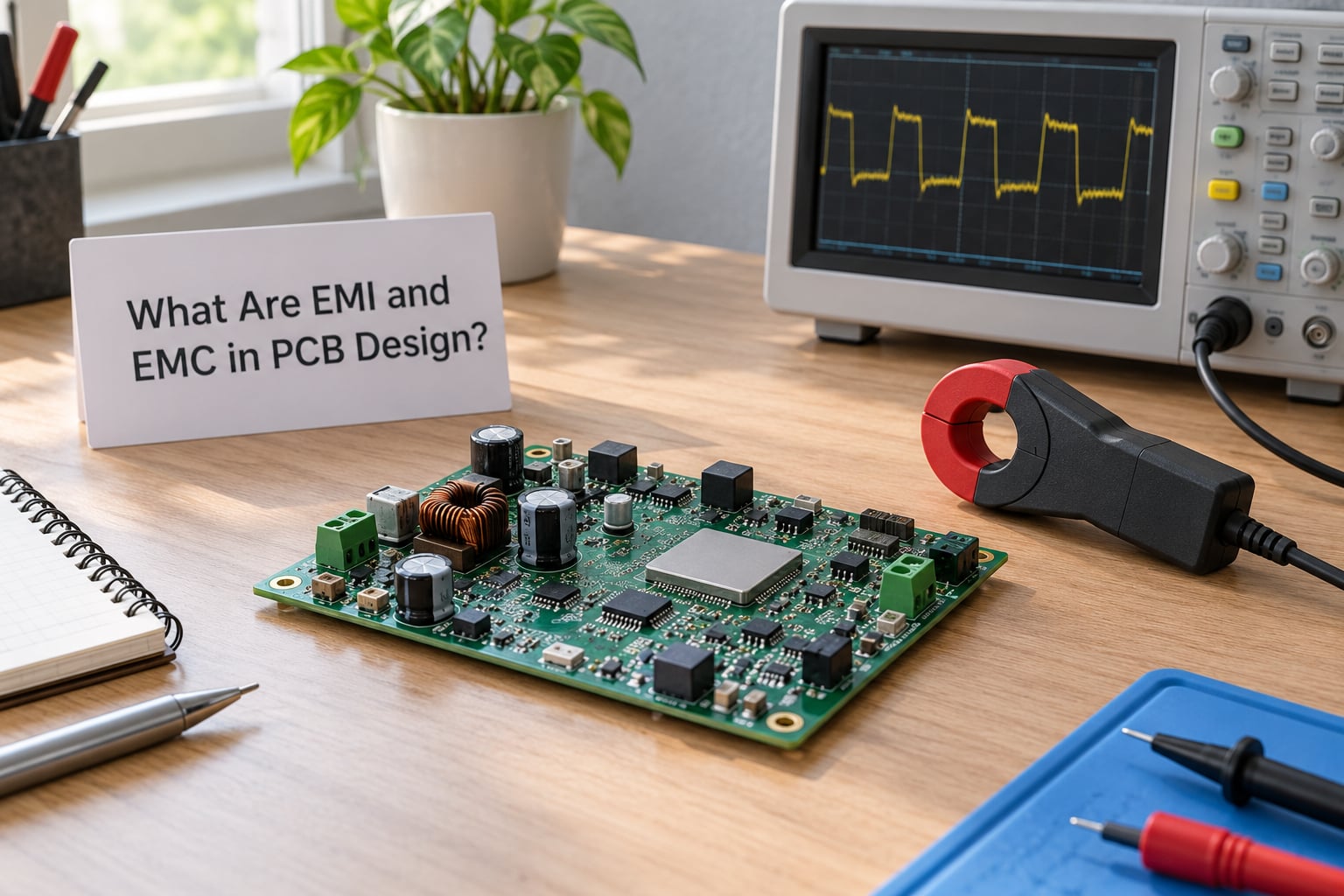
EMI, electromagnetic interference, is the unwanted electromagnetic energy a circuit produces and releases into its surroundings. EMC, electromagnetic compatibility, is the ability of a device to work in its environment without disturbing anything else and without being disturbed.
In practice you have two directions to worry about. Emissions push energy out: radiated into free space from traces, planes and cables, or conducted down the power and signal wires that leave your board. Immunity is the reverse, the ability to keep operating correctly when an outside field, a discharge or a switching surge hits the board.
Both matter for a PCB product. A module that radiates too much fails the emissions test. A sensor board that browns out when a motor starts next to it fails the immunity test even though it emits almost nothing. And both are decided long before certification: by which rails are quiet, how the switching loops are shaped, whether return paths are continuous, and how the cables are treated at the connector.
| Term | What it measures | Direction | Typical failure |
|---|---|---|---|
| Radiated emissions | Field strength in free space, measured in dBµV/m | Board to world | Fails a 3 m chamber scan near a switching fundamental |
| Conducted emissions | Voltage and current on the AC or DC power lines, measured in dBµV | Board to power line | Fails on a LISN at the switching frequency or a harmonic |
| Immunity | Correct operation while an external stress is applied | World to board | Reset, corrupted ADC data or a dropped link during an ESD hit |
EMI and EMC Basics for PCB Designers: Where Problems Come From
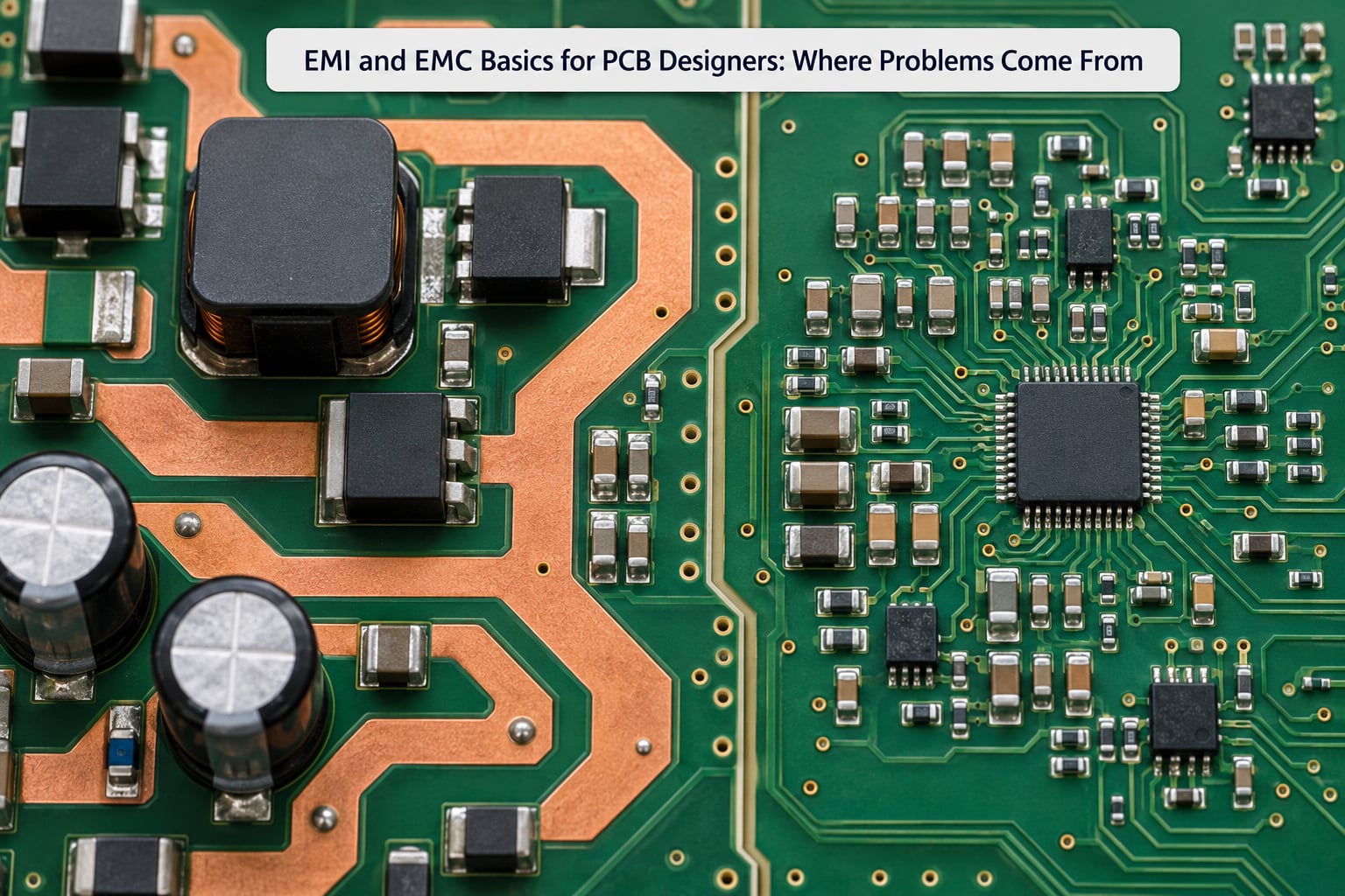
The common mistake is to think the energy travels in the copper. It does not. Signal energy lives in the electric and magnetic fields between a trace and its return plane, and the copper pair behaves like a waveguide. That is why a trace that is perfectly fine for signal integrity can be a radiator, and why the same trace radiating badly is often fixed by changing what sits underneath it rather than the trace itself.
Three mechanisms account for almost everything you see on a spectrum analyser.
Conducted interference
Common-mode current flows in the same direction on every conductor in a cable, including protective earth. It is not a problem the cable was designed to carry, so it radiates, and on a DC input it rides straight out of the board and down the power lead. This is the mechanism behind most conducted emissions failures, and the reason the return path matters more than the forward path.
Radiated electric fields
A trace that rises quickly relative to its return plane drives voltage into the space between them. Faster edges mean more high-frequency content, so the radiated electric field grows with edge rate rather than with clock frequency.
Radiated magnetic fields
Any current loop has a magnetic field around it. Shrink the loop and the field collapses. This is why loop area is the single most reliable number on any EMI checklist.
That leads to the idea designers most often get wrong. A board built around a 16 MHz microcontroller can emit significant energy near 500 MHz, because the interesting content comes from the edge, not the clock. A useful approximation for the highest significant harmonic is f(max) = 0.5 / (trise + tfall), with rise and fall times in nanoseconds giving the result in gigahertz. A 1 ns edge therefore has meaningful content to roughly 500 MHz, and a 100 ns PWM edge to about 5 MHz. The same figure explains why a slow 16 MHz MCU and a 200 MHz part built with the same layout can behave very differently.
Impedance mismatches add to this. An unterminated clock line, a stub, or a via transition with no ground via next to it reflects energy back down the trace, and the reflected edge is another emission event. A trace that crosses a split in its reference plane forces the return current to detour, and that detour is an antenna.
What Is the Difference Between Emissions and Immunity?
Emissions are about what your board gives out. Immunity is about what your board survives. They are measured with different equipment, at different frequencies, and are fixed with different design moves, which is why treating them as one number is a mistake.
Emissions testing is passive. A spectrum analyser with a LISN watches your power port, or an antenna watches the board inside a chamber, and you look for peaks that exceed a limit line. Immunity testing is active. The lab applies something to the board: a contact discharge, an EFT burst, a surge, or a field at 3 V/m, and then checks whether the product still behaves.
A board can pass one and fail the other. A well-laid-out switching converter with a long unprotected input cable can be radiated-quiet and conducted-noisy. A precision analog front end with a floating shield and no ground stitching can emit almost nothing and still reset every time somebody touches the connector.
The layout levers do overlap, though. Continuous return paths lower emissions and raise immunity at the same time, because a signal with an intact return is both quieter to receive and harder to disturb. That is why grounding practice is the first place to look for either problem.
Which PCB Design Decisions Have the Biggest EMI Impact?
Stackup and loop area dominate. Everything else is a refinement of the same two ideas: keep the field between a trace and its return, and keep the area of every current loop small.
Stackup and layer count
A four-layer board with a solid ground plane directly under the signal layer is the cheapest large improvement available. Typical experience puts a two-layer board radiating 10 to 20 dB above a comparable four-layer board in the same frequency band, because the fields are no longer trapped between the traces and the nearest copper.
On a two-layer board you can partly recover that by keeping ground pours on both sides, by keeping return path under the trace, by using the 3W rule, and by treating every signal as slow. It works for a low-speed design. It gets uncomfortable as soon as you route anything with sub-nanosecond edges.
| Stackup | Field containment | Typical emissions | Where it fits |
|---|---|---|---|
| 2 layer | Fields escape on both sides | Highest, often 10 to 20 dB above a 4-layer design | Low-speed controls, sensor boards under 1 MHz |
| 4 layer, signal-ground-power-signal | Fields trapped against the ground plane | Baseline for most industrial products | Most new designs at any clock speed |
| 4 layer, signal-ground-signal-power | Good for signals, weaker plane integrity for the return | Between the two, watch the top reference | Boards with a quiet top analog section |
| 6 layers or more | Inner planes plus tight stripline | Lowest, at higher BOM and routing cost | High-speed interfaces, dense mixed signal |
Switching loop area
In a switching converter the input capacitor, the high-side device and the low-side device form a pulse of current every cycle. Keep that loop under about 3 cm² and you will usually stay well under the 100 mm² figure that shows up in most generic layout rules. The same reasoning applies to gate loops, to the pulse loop around a relay, and to the current loop of a linear regulator’s output capacitor.
Edge rate
You cannot slow the silicon, but you can stop driving the net, remove the unnecessary via, split the load into two chips, or place a small series resistor or RC on the edge. Spreading a 4 ns edge into two 8 ns halves moves energy to lower amplitude at higher frequency, which is often a better trade than the raw number suggests.
Microstrip versus stripline
Microstrip has an open field above it and is easier to probe and rework. Stripline sits between two ground planes, so the field is contained, crosstalk drops, and the radiated field is much lower. For a high-speed or high-emission region on a four-layer board, stripline between the two inner planes is the single easiest win available.
Plane cuts and edges
A trace that crosses a gap in its reference plane forces the return current to flow around the gap, and that loop is an antenna. When a plane has to be cut, bridge it with stitching vias along the signal path. The same logic applies to the board edge: keep the plane continuous to within a few millimetres of the edge, and keep traces away from the edge so the outer copper is not acting as a radiating slot.
Cables and connectors
A cable is an antenna. A quarter-wave resonant length at 75 MHz is about 4 metres of cable, while a USB lead is about 1.5 metres, and at that length it is resonant across a wide band where it re-radiates whatever common-mode current your board pushed into it. This is the most common real-world failure mode, and it is why the connector is an EMI design decision rather than a mechanical one.
How Do Grounding and Return Paths Reduce EMI?
A return path is not a wire to ground. It is the conductive structure that the return current follows to close the loop, and that structure is what sets the field geometry. Get it right and most other problems shrink.
It helps to keep three different things separate in your head. The signal return is the reference plane under a trace, and its only job is to be continuous under that trace. Chassis ground is the metal enclosure, which is the reference for radiated fields and the thing that a shield is bonded to. Protective earth is the safety ground on the mains side, which carries fault current and has nothing to do with signal return quality.
When the return path is broken, two bad things happen at once. The return current detours around the gap, which lengthens the loop and increases the radiated magnetic field. And the inductance of the detour develops a voltage across it, so the receiving circuit sees a signal that is not the one you routed.
Stitching vias are the fix. Placing ground vias along the path of a return current, typically every 5 to 10 mm, gives the current a nearby low-inductance route and stops it wandering. The same vias tie a ground pour to a ground plane, and tie a shield can to chassis ground so the shield actually intercepts fields rather than floating and reradiating them.
Should you split the ground plane between analog and digital?
Almost never, and this is the question that comes up most often in design reviews. A split forces every signal crossing the boundary to lose its return path, so the return detours, and you have created exactly the loop you were trying to avoid. The current practice is a single solid ground plane, with analog, digital, power and I/O circuits kept physically separated on that plane and joined at one deliberate point where it makes sense.
| Approach | Return path at the boundary | Result | Verdict |
|---|---|---|---|
| Solid plane, separated regions | Continuous underneath | Small loops, low radiation, easy to analyse | Default choice |
| Split analog and digital ground, joined at one point | Continuous only at the star point | One crossing carries a large detoured loop | Only with a good reason, such as a high-resolution converter |
| Fully split, never rejoined | Broken | Radiating loop at every crossing, ground bounce | Avoid |
Where people are tempted to split the ground is around a high-resolution ADC or a reference supply, and in those cases a single-point join often beats a full split. The rest of the board still shares one solid plane. And any split you do keep should be bridged with a network of 1 nF to 100 nF capacitors plus a resistor, so that the high-frequency return can cross even though the DC ground cannot.
How Can PCB Designers Control EMI with Layout and Components?
Layout does most of the work. Components handle what layout cannot, and they are cheap to change late in the design, which makes them the right first tool when a fix is needed without a re-spin.
Decoupling close to the pin
Put a 0.1 µF and a 1 nF ceramic within about 2 mm of each supply pin, with the via for the capacitor next to the pin rather than next to the capacitor. The 1 nF handles the fast edge, the 0.1 µF handles the mid-band, and the via inductance is the reason distance matters more than capacitance here. A decoupling capacitor two centimetres away is a capacitor in name only.
Snubbers on switching nodes
An RC snubber across a switching node, or an RCD clamp on a power stage, damps the ringing that adds a clean, easily measured emission peak. It also dissipates real power, so size it from the ringing frequency you see on a probe rather than from a habit.
Series termination
A 22 to 33 Ω resistor in series with a clock or long fast edge line reduces reflections and slows the edge, which cuts harmonics. On a 1 ns edge into a mismatched load this is often the cheapest 6 to 10 dB you will get.
Ferrite beads and common-mode chokes
A ferrite bead in a supply line blocks RF while passing DC, and a common-mode choke on a cable blocks the current that flows in the same direction on all conductors. Be careful with impedance: a bead has a self-resonance, and above it the bead is an inductor, not a suppressor. Pick one whose self-resonance sits above the frequency you are trying to remove.
Y-capacitors and connector filtering
A small capacitor from each line to chassis at the connector shunts common-mode current onto the enclosure instead of down the cable. It has to be a safety-rated part if the line is mains, and the connection to chassis must be a real connection, not a hairline trace.
Shielding, and where it belongs
Shielding reduces radiated field and improves immunity, and it does not fix a bad layout. A shield can only intercept energy that reaches it, and it is only as good as its bonding: the contact spacing rule of λ/20, the seam gap, and the aperture size all matter, and a can floating 2 mm above the board does very little. Treat it as a last step after stackup, loop area and return paths are right, and bond it with vias placed at less than λ/20 spacing around its perimeter.
Fixing EMI on a board that is already built
Before you respin, try the cheap options, because several of them are reversible. Add a snap-on ferrite or a small air-core common-mode choke wound on the cable, which forum users report fixing conducted failures without touching the board. Bridge a plane split with a capacitor. Slower-edge replacement of a buffer often moves several harmonics. Where a radiated peak has a known source, copper tape over a specific trace or region can confirm the diagnosis even if it is not the final fix.
How Do You Test EMI and EMC Before Compliance Testing?
Pre-compliance testing is a design loop, not a formality. You are looking for peaks you can point at, so you can change one thing and see whether the number moves.
- Define the product. Note the power rails, the cable lengths, the intended enclosure, the ports that leave the board, and the standard and market you are aiming at. Emissions limits depend on the product class, and an unshielded board test means very little if the real product is metal.
- Inspect the design before you power it. Check return path continuity, stitching vias across every split, decoupling distance, loop areas, and whether the SW node copper is as small as the datasheet allows.
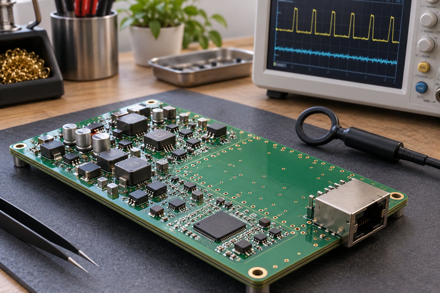
- Set up a near-field scan. A small loop probe and a shielded or filtered oscilloscope will find a radiating trace or inductor in minutes, and the sharpest peak usually maps to a specific component within a few centimetres.
- Measure conducted emissions on the DC port. A cheap conducted pre-compliance setup is a LISN or a current probe plus a spectrum analyser, and it will find problems that a chamber scan hides.
- Compare against the applicable limit line and write down every peak in dBµV/m or dBµV. A log is what lets you tell whether a change helped.
- Change one thing, re-measure, and keep the change if the peak moves. Shielding and filtering go in last, on top of a layout that already works.
| Observed peak | Likely physical cause | First thing to check |
|---|---|---|
| Exactly the switching frequency and its low harmonics | Switching converter input or power loop too large | Input capacitor distance, SW node copper area |
| Broad rise across a wide band | Fast edges on a long trace, or an unrouted return | Edge rate, series termination, return continuity |
| Only when the cable is attached, and it scales with cable length | Common-mode current pushed out through the cable | Common-mode choke, Y-caps at the connector |
| A single sharp peak, easily localised by a near-field probe | Inductor or transformer radiating into a floating shield | Shield bonding, keep-out copper around the device |
| Strong at twice or three times the clock | Harmonic series from a square-ish edge | Slower-edge part, RC on the net |
| Peaks that move when you move the board or cable | Antenna effect from a resonant structure | Board edge copper, trace length, chassis bonding |
Immunity gets a pre-compliance pass too, and it is mostly a review exercise. Check that the ESD path has a short, wide route to chassis, that the surge and EFT entry points have series impedance or filtering in front of them, and that no critical signal runs unprotected across a long cable. A read-only register or a debounce on a reset line buys you more practical immunity than any filter.
What EMC Standards May Apply to a PCB Product?
There is no universal EMC standard for a PCB. The applicable document depends on the product class, the market it ships into, the ports it exposes, and the environment it will be used in. What you can do at design time is know the candidates, and the table below covers most of the ones a board designer meets.
| Product or market | Emissions | Immunity | Typical test |
|---|---|---|---|
| Unintended radiators, United States (FCC Part 15, Subpart B) | Class A or Class B | Not part of Part 15 B | 3 m chamber or 30 m, radiated |
| IT and telecom equipment, Europe and CISPR countries | CISPR 22 / EN 55032 Class B | EN 55035 or IEC 61000-6-1 | Chamber plus LISN on the AC and DC ports |
| Audio and video, broadcast receivers | CISPR 18 or CISPR 32 Class B | EN 55020 | Radiated and conducted on the mains port |
| Automotive electronic sub-assemblies | CISPR 25 | ISO 11452 and ISO 7637, CISPR 25 class per application | Component-level conducted and radiated measurement |
| Laboratory, medical and industrial measurement | EN 61326-1 / CISPR 11 group and class | IEC 61000-4-x | Group and class determine the limits |
| Generic component-level immunity | Not applicable | IEC 61000-4-2 ESD, 61000-4-4 EFT, 61000-4-5 surge, 61000-4-3 radiated RF | Applied at the port or enclosure |
Check the current edition in force for your market before you design to it. Limits and test setups get revised, and the class your product falls into is a commercial decision as much as a technical one.
If you want one book behind all of this, Henry W. Ott’s Electromagnetic Compatibility Engineering is the reference that comes up most often in engineer forums, and it is the one I would put on the desk before starting.
Frequently Asked Questions
Is EMI the same as EMC?
No. EMI is a problem: the unwanted electromagnetic energy a circuit radiates or conducts, both inside and outside the device. EMC is a property: the ability of that device to work in its environment without disturbing other equipment and without being disturbed. A product can have EMC while still producing measurable EMI, and a product with strong EMC may still need filtering to keep its own emissions inside the legal limits.
What is the most common cause of EMI on a PCB?
A large high-frequency current loop, usually a switching converter with its input capacitor too far from the switching devices, or a trace whose return path is broken by a plane split. Closely behind it come fast edges on long unrouted returns and cables carrying common-mode current out of the board. The first three are decided in the schematic and the layout, which is why the fix is nearly always made there.
Do I need a separate ground plane for analog and digital circuits?
Usually not. Current practice is one solid ground plane with analog, digital, power and I/O sections kept physically separate on that plane, rather than a split. A split forces every signal crossing the boundary to detour its return current, which creates exactly the radiating loop you were trying to avoid. Separate planes are worth considering around a high-resolution converter or a precision reference, joined at a single deliberate point.
Does shielding solve EMC problems?
It reduces radiated field and helps immunity, but it is a mitigation, not a fix. A shield only intercepts energy that reaches it, and it works according to how it is bonded: contact spacing at less than one twentieth of the wavelength, a tight seam, and a real connection to chassis ground. A can floating above the board does very little, and shielding a board with a 10 cm² switching loop will simply enclose the antenna.
When should I test a PCB for emissions and immunity?
Before you release it for fabrication, and again on the first article. Pre-compliance with a near-field probe, a current probe and a spectrum analyser takes an afternoon and routinely finds a radiating loop in minutes. Waiting for a chamber test means a failed re-spin, a new round of chamber time, and a delay to certification, which is the single most expensive way to learn a layout mistake.
Can PCB layout alone guarantee EMC compliance?
No, and anyone who promises it is overselling. Good layout, a sensible stackup, continuous return paths, controlled loop area and treated cables get you most of the way, and they are what determine whether you pass first time. The remaining margin usually comes from enclosure design, cable and connector treatment, and sometimes shielding. Layout is the part you control fully, so it is where the effort belongs.
Conclusion: Start EMI and EMC Planning at Schematic Stage
If you do three things this week, make them these. Mark every noisy circuit and every sensitive circuit on the schematic, so the layout partitions them by function instead of by convenience.
Then plan the current loops and the return paths before routing anything, keep the switching loops under about 3 cm², and decide at the schematic stage where the filtering and the connector treatment will live, because those components need board area and ground references that are much harder to add later.
Finally, measure before you fabricate. An afternoon with a near-field probe on the first article tells you which loop to fix, and it costs far less than a chamber re-test. The design rules behind all of this are worth reading once more before you place the first component, and the standard that will apply to your product is worth checking early, since the emissions class changes how much margin you need.