Boundary scan testing is a standardised method, defined as IEEE 1149.1 and commonly called JTAG, for checking the connections between integrated circuits on a printed circuit board by shifting test data through dedicated boundary scan cells inside the ICs. No physical probes, no bed-of-nails fixture, and it works on ball grid arrays and fine-pitch parts that no probe can reach.
This guide walks through the architecture, the test sequence, the fault classes it finds, and the design rules you need to follow so the technique actually works on your board. It is written for hardware and PCB engineers who have heard of JTAG but never designed a scan chain.
One quick note before we go further. If you arrived here searching for software testing, this is the wrong article. Hardware boundary scan has nothing to do with boundary value analysis, the software quality technique that checks input and output limits. Different field, same words.
Table of Contents
- What Is Boundary Scan Testing and Why Is It Used?
- How Does Boundary Scan Testing Work?
- How Do JTAG, TAP Controllers, and Boundary Registers Work Together?
- What Is the Four-Wire JTAG Connection?
- What Instructions Are Used in Boundary Scan Testing?
- How Is a Boundary Scan Test Performed Step by Step?
- How Does Boundary Scan Locate Wiring and Interconnect Faults?
- What Does a Boundary Scan Test Report Look Like?
- What Are the Main Benefits of Boundary Scan Testing?
- What Are the Limitations and Common Failure Points?
- How Do You Add Boundary Scan Support to a PCB Design?
- Frequently Asked Questions
- Is boundary scan testing the same as JTAG testing?
- What faults can boundary scan testing detect?
- Does boundary scan replace in-circuit testing?
- Which devices support boundary scan testing?
- Is boundary scan testing required for every PCB?
- Conclusion
What Is Boundary Scan Testing and Why Is It Used?
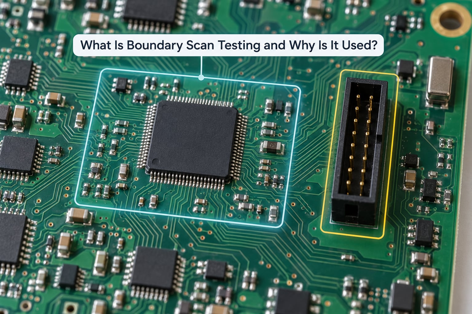
Boundary scan testing checks interconnections at the solder joint and trace level. Each scannable IC carries a small state machine and a set of boundary scan cells, one per digital pin, that can either drive a known logic level onto that pin or capture the level arriving on it. A controller shifts patterns into the driving cells, lets the board settle, captures what the receiving cells see, and compares it with what the design netlist says should be there.
The reason the industry adopted it is simple: physical access disappeared. A QFP with 0.5 mm pitch has pads narrower than a probe tip can land on without a custom fixture, and a BGA hides every joint under the package. The nets that used to be trivially testable are now the ones you most want to test. Boundary scan puts the test access inside the silicon, where the packaging density cannot hide it.
What it catches in practice:
- Open circuits, including a lifted BGA pad that never bonded to the board
- Shorts and solder bridges between adjacent nets
- Stuck-at-0 and stuck-at-1 conditions on a driver pin
- Missing, wrong or misoriented devices, caught by reading the IDCODE
- Wiring mistakes that survived schematic review, such as a net mapped to the wrong pin
It also gives you a second and third job with the same four wires. Those pins can load a bitstream into an FPGA, write a bootloader into flash, and act as a debug port into a microcontroller. The scan chain that finds a bridge on a production line is the same chain that flashes the board at end of line.
How Does Boundary Scan Testing Work?
The mechanism is a shift register stitched through every scannable device on the board. Each boundary scan cell holds one bit of state plus a control section, and those bits are connected in series so data walks from the controller into the first device, through that device’s cells, into the next device, and back out to the controller.
Around that bit sits a small control multiplexer with a few distinct functions. The capture function copies the logic level on the physical pin into the cell. The update function copies the cell’s stored value out onto the physical pin, which is how a cell drives. The shift function moves the captured bit along the chain, and the select function chooses which of those behaviours is active based on the instruction currently loaded.
Here is a small worked example. Suppose U1 pin 40 drives net N1 and U2 pin 12 receives it. The tester loads the EXTEST instruction into both devices, then shifts a pattern where U1 pin 40 is set to drive 1 and U2 pin 12 is set to capture. It moves to the capture phase, and U2 pin 12 latches the level currently present on N1.
Three outcomes are possible. If U2 captures 1, the connection is intact. If it captures 0, either the driver cell is not driving or the net is open somewhere between the two pins. Reverse the roles, drive from U2 pin 12 and capture at U1 pin 40, and the direction of the fault becomes clear. A one-way failure means an open on the driving side or a dead driver; a two-way failure points at the net itself.
That two-way pattern is why boundary scan produces diagnosis rather than just a pass or fail. You do not get told the board is bad, you get told that net N1 fails to conduct in both directions and that U1 pin 40 is the driving pin in the failing pattern.
How Do JTAG, TAP Controllers, and Boundary Registers Work Together?
Every scannable device has a Test Access Port, which is the small group of pins that gives a controller access to the internal test logic. Inside sits the TAP controller, a 16-state state machine defined by the standard. It reads one serial bit of control on every clock edge and decides what the rest of the test logic should be doing next. Nothing about the test happens unless the TAP controller has been walked into the right state first.
Two registers sit under that controller. The instruction register holds the command telling the device what to do next, such as EXTEST or BYPASS. The data registers hold the actual test data, and the boundary scan register is one of them, made of one cell per pin. Selecting which data register is active is the job of the instruction the TAP controller shifts in.
The cycle that matters repeats constantly. The controller moves the TAP into the shift instruction state and shifts a new instruction through the instruction register of every device in the chain. It then selects the data register named by that instruction, drives one or more clock cycles to let the cells capture, and shifts the captured bits out for comparison.
Because all devices share TCK and TMS, they all change state at the same time, which is how a single controller stays in lockstep with a chain of a dozen or more parts. The trick that makes this practical is the BYPASS instruction. Any device that is not part of the current test gets a one-bit bypass register inserted into the chain, so the tester can shift past it without knowing anything about its internal logic. The chain stays a straight shift register no matter how mixed the board is.
What Is the Four-Wire JTAG Connection?
Four signals carry everything. Three of them are mandatory, and a fifth, TRST, is optional and asynchronous. There is no separate reset requirement even without TRST, because the TAP controller can be walked to its Test-Logic-Reset state through TMS alone.
| Signal | Name | Direction | Purpose | Typical failure mode |
|---|---|---|---|---|
| TCK | Test Clock | Input to device | Clocks shift, capture and update operations across the whole chain | Excessive fanout or skew between distant devices causes shifted data to arrive at different times |
| TMS | Test Mode Select | Input to device | One serial bit per clock that walks the TAP controller state machine | Floating input with no pull resistor, so noise moves the state machine to an unknown state |
| TDI | Test Data In | Input to device | Carries instructions and shifting-in data toward the first device in the chain | Swap with TDO during wiring, which inverts the entire bit sequence |
| TDO | Test Data Out | Output from device | Carries captured data and responses back toward the controller | Two TDO lines shorted together when a designer forgets that outputs cannot be daisy chained |
| TRST | Test Reset | Input to device | Optional asynchronous reset of the TAP controller, active low | Held in the wrong state, or pulled low by a supply rail collapsing during power-up |
Devices connect in a daisy chain. TDI from the controller goes to the first device, that device’s TDO goes to the second device’s TDI, and the last device’s TDO returns to the controller. TCK and TMS fan out to every device in the chain, which is why those two lines need buffering when the chain is long or physically spread out.
Buffering is not optional on a big board. Clock skew between a device near the connector and a device at the far edge can be enough to corrupt a bit at high shift rates. The usual fix is a TCK buffer per device, which equalises delay. TMS can run a little slower because it only changes state every few cycles.
What Instructions Are Used in Boundary Scan Testing?
The instruction loaded into the instruction register decides what a device does for the rest of the test. Three instructions are mandatory in every IEEE 1149.1 device, and the rest are optional or vendor-defined.
| Instruction | Status | What it does | Typical use |
|---|---|---|---|
| EXTEST | Mandatory | Selects the boundary scan register so cells drive their output pin and capture their input pin | Interconnect test, pin-level fault detection, board bring-up |
| SAMPLE/PRELOAD | Mandatory | Captures the current state of the system outputs into the boundary scan register for shifting, without changing what the pins drive | Sampling a running system for debug, and preloading cells before a test |
| BYPASS | Mandatory | Selects a one-bit register so the chain can shift through a device that is not under test | Chain navigation, isolating a device, chain integrity checks |
| IDCODE | Optional | Shifts out the manufacturer, part number and version bits the device holds in a dedicated 32-bit register | Device presence, orientation and part verification |
| INTEST | Optional | Runs the device’s own internal test while the boundary cells drive a known pattern | Combining internal logic test with interconnect test |
| USER1 | Vendor | Vendor-defined instruction, commonly a private data path or a device-specific function | Programming, serial flash access, private debug channels |
A short example of why the combination matters. A tester uses BYPASS to shift a known pattern through the whole chain and confirm the bits come back intact, which is a continuity check of TCK, TMS, TDI and TDO themselves. It then switches to IDCODE to read every device, then to EXTEST to run the interconnect patterns. The first two steps often happen automatically before you ever ask for an interconnect test.
How Is a Boundary Scan Test Performed Step by Step?
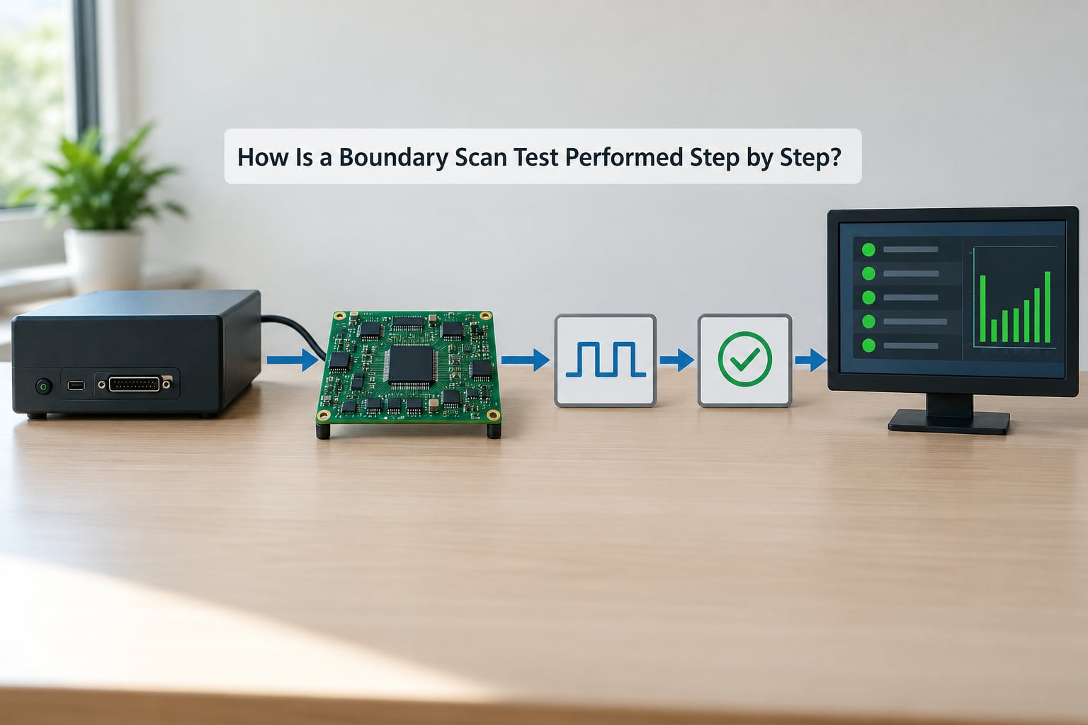
The flow below is what a production test system does once the fixture is built and the test program is generated. The specific menus differ between tools, but the sequence is the same everywhere.
- Apply power and confirm the board is alive. The tester checks supply rails and any power-on self-test before touching the chain. A board that fails here should never be scanned, because a partly powered device can shift nonsense.
- Reset the TAP and detect the chain. The controller walks to Test-Logic-Reset, then shifts an all-ones pattern through the chain. Anything that does not come back as 1 indicates a broken device, a wiring problem or a chain-order mistake in the model.
- Read the IDCODE of every device. This confirms which part is on which link of the chain. A mismatch here usually means the device order in the test program does not match the board.
- Load EXTEST into the boundary scan registers. Known patterns go into the driving cells while the receiving cells are set to capture.
- Apply settle time, then capture. A short pause lets the board settle before the capture phase latches the received values.
- Shift the captured data out and compare. The tester matches observed against expected for every net it can observe.
- Retest and diagnose. Failing nets are tested again, including in the reverse direction, to separate opens, shorts and driver problems.
- Report and route. Pass, fail, or fail with a diagnosis. A failing board is usually held for rework rather than scrapped, since the fault is named.
Generating the patterns is mostly automatic, and that is where the input files matter. You give the tool the board netlist and the BSDL file for every device, which is a vendor-supplied text file describing the boundary scan register pin order, the instruction opcodes and the device’s IDCODE. A test program generator combines them into patterns.
For a mid-sized mixed-signal board, a vendor tutorial reports generating a test of 5,638 nets and 19,910 pins in about 23 seconds, with net coverage above 60 percent on a design that was never laid out for test. The BSDL is the piece that is hardest to obtain, because it is usually published on the manufacturer’s site rather than included with the part, and when it is missing, engineers end up asking for it on vendor forums.
How Does Boundary Scan Locate Wiring and Interconnect Faults?
The whole diagnosis comes down to comparing an expected response with an observed one, and then re-running the comparison with the roles of the two ends of the net swapped. That single extra step is what separates a fault class from a symptom.
Consider four nets running between two devices, tested with U1 driving and U2 capturing:
- Net 1, open. U1 drives 1, U2 captures 0. Reverse the direction and the fault repeats, so the net is broken somewhere along the trace, the via or the joint. The tester then narrows the location by testing sub-segments where extra boundary cells exist, for instance on a resistor divider in the middle of the run.
- Net 2 shorted to Net 3. The tester drives a 1 on Net 2 and a 0 on Net 3, and every pin on both nets captures 1. That wired-AND result is the signature of a bridge: the two nets are joined, so anything driving high wins. Seeing it on both nets at once tells you it is a short between those two, not a stuck driver.
- Net 4, stuck-at on a driver. The driver cell is set to 0 and the receiving cell still captures 1, and the same thing happens in reverse. A fault that does not follow the test pattern is a stuck pin, not a wiring problem.
Two more classes fall out of the same data. A missing pull-up or a wrongly fitted bias resistor shows up as a net that reads a state nobody drove, and an incorrectly wired device shows up in the IDCODE step rather than the EXTEST step, which is why that step always runs first.
It is worth knowing where the resolution stops. Boundary scan reports nets, not coordinates. Naming the failing net is genuinely useful for rework, but the technician still has to find the physical location, and for that you pair the result with AOI or X-ray inspection of the same board.
What Does a Boundary Scan Test Report Look Like?
A test report is small, and the useful version is a list rather than a chart. Typical fields are a pass or fail verdict, total nets tested, nets covered by boundary scan, nets not covered and why, and a list of detected faults with pin-level detail for each one.
For every detected fault you normally get the net name, the driving pin and the receiving pin, the expected and observed value, the fault class the tool assigned, and a confidence value describing how certain the tool is about the diagnosis. That confidence figure is worth reading. A tool that retests a failure in both directions and sees a clean open pattern is more certain than one reporting a single mismatched bit.
Typical fault classes in a report are open, short between two named nets, stuck-at, incorrect device, and untested. The untested entry matters just as much as the failures, and it is the one most reports bury. Nets running to analog components, memory devices with no scan support, or a mixed-signal block with no boundary cells at all cannot be observed, and a report that says 60 percent coverage is telling you that 40 percent of the board was never checked by this method.
Two limits on interpretation. A pass means the scanned digital interconnects behaved as expected under the patterns used, which is not the same as the board working. And a fault list is not a repair instruction, because one bad solder joint can show up as a fault on several nets at once, and one short can light up every net between the bridged pair.
What Are the Main Benefits of Boundary Scan Testing?
The coverage argument comes first. On a board with a large BGA and fine-pitch parts, a bed-of-nails fixture can often only reach a fraction of the nets, and the fraction it cannot reach is the fraction that carries the most risk. Boundary scan reaches the joints under the package, which is where solder defects concentrate.
There is a fixture cost angle too. Every bed-of-nails fixture is a custom mechanical and electrical design that has to be maintained as the board changes, and boundary scan needs only a connector, a cable and a controller. For low and medium volume lines, that difference is usually the deciding factor, and for prototype work it is the reason boundary scan is the only practical option at all.
Debugging is the underrated benefit. Before boundary scan, finding a bridge on a prototype meant cutting traces and bisecting by hand. With a scan controller on the bench, a fault that is invisible to a multimeter because two nets sit between two inaccessible pads becomes a named net in seconds. Several devices that support it can also be told to hold a safe state or drive a reset line, which stops a bad part from fighting the good ones while you look.
Test time is a real number, not a marketing one. An interconnect test on a mid-sized board typically completes in seconds, because the patterns are generated from the netlist rather than written by hand.
Finally, the same infrastructure serves three other jobs. In-system programming of flash, CPLDs and FPGAs happens over the chain. Source-level debugging through a JTAG emulator uses it. And field service teams use it to read a fault off a board that has already left the factory, which is only possible because the four test wires are still connected and documented.
What Are the Limitations and Common Failure Points?
Boundary scan is a digital interconnect test, and it stays inside that boundary. It does not check analog component values, it does not measure power and ground integrity, it does not verify RF behaviour, and it does not exercise the internal logic of the chips themselves. A board can pass boundary scan and still fail functional test, and on a mixed-signal design that is the normal outcome rather than a surprise.
The comparison below is the honest version of where each method sits.
| Method | What it sees | Analog coverage | Setup cost | Best fit |
|---|---|---|---|---|
| Boundary scan | Digital interconnects, device presence, pin faults | None | Low, no custom fixture | BGA and fine-pitch digital boards, prototype debug, ISP |
| Bed-of-nails ICT | Net connectivity plus many analog values | Good | High, custom fixture per board | High volume production of mixed-signal boards |
| Flying probe | Net connectivity, some analog values, no fixture | Moderate | Low, no fixture but slow | Prototype and low volume work |
| AOI | Solder joint appearance and placement | Visual only | Moderate | Finding the physical location of a defect |
| X-ray | Hidden joints under BGAs and QFNs | Visual only | High | BGA solder inspection and failure analysis |
| Functional test | Whether the board does its job | Indirect | Moderate | End-of-line verification of behaviour |
These methods are complementary rather than competing. The common production flow runs boundary scan first because it is fast and names the fault, then AOI or X-ray to find it physically, then functional test to confirm the repair worked.
When boundary scan itself fails, the causes are mostly practical:
- Chain integrity errors. One failed or badly soldered device can make the entire chain unreadable, which is the most common practitioner complaint about the method. The workaround is chain partitioning, where you split a long chain so a failure affects fewer devices.
- Missing or wrong BSDL. A wrong BSDL gives you the wrong pin order, and the results look like a board full of opens.
- Unsupported devices. A memory or analog block with no boundary cells caps your achievable coverage, and no amount of testing changes that.
- Unbuffered TCK. Skew on a long chain corrupts shifted data and shows up as random, unrepeatable failures.
- Floating JTAG inputs. An unconnected TMS or TRST lets noise drive the state machine somewhere unpredictable.
- Poor fixture contact. A dirty or worn pogo on the JTAG connector breaks the whole test, since the connector carries every bit of the chain.
It is also fair to say why boundary scan is less visible than it once was. Most development boards give each CPU, FPGA and PHY its own chain, and most engineers use those chains for debugging and programming rather than for board-level test. That is a tooling and habit issue, not a limitation of the technique. The hard part of boundary scan is the DFT work that happens before layout, and that is the part that quietly gets skipped when a board is small or when a prototype has to be turned around this week.
How Do You Add Boundary Scan Support to a PCB Design?
Boundary scan is decided in the schematic, not in layout, and most of the work is a checklist rather than a routing problem. Work through it in this order before you release the layout.
Pick scannable parts where you can. Choose devices with boundary scan support and a published BSDL before you commit to a part, not after. A microcontroller with 800 pins and no boundary cells gives you no interconnect coverage on any net that only reaches that device.
Check the BSDL situation early. Confirm the file exists on the manufacturer site and that the boundary scan register pin order in it matches your symbol and footprint pin numbering. This mismatch is a common source of tests that pass on one board and fail on the next.
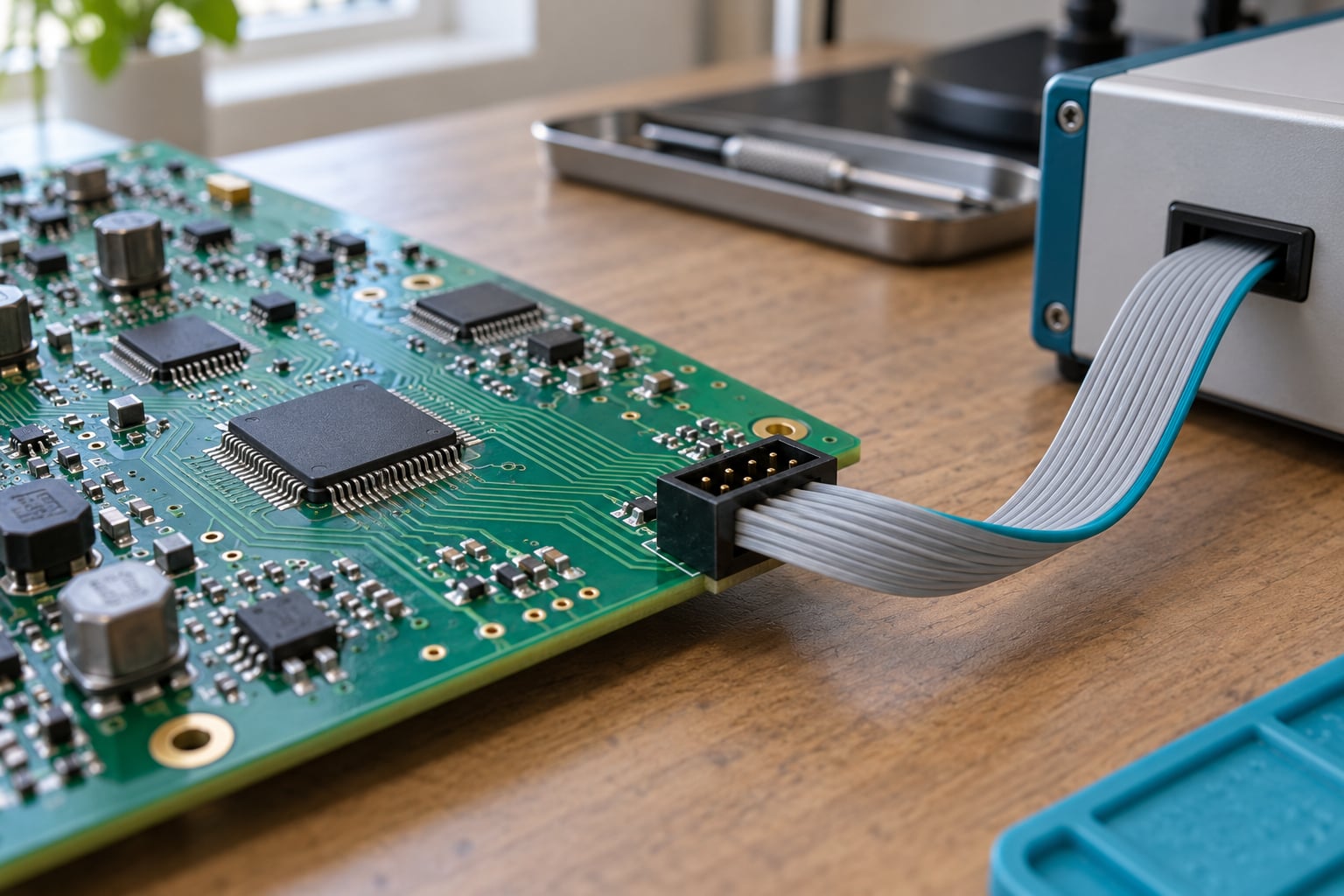
Bring the TAP out to a connector. A standard 2 by 5 pin 1.27 mm header with the four mandatory signals plus TRST is the conventional choice, with TCK, TMS, TDI and TDO labelled on the board. Put it where a fixture pogo or a cable can reach it without a mechanical change.
Set the chain order deliberately. The serial order in the model must match the physical order on the board, and it changes with every component move. If the chain is long, plan to use separate chains per FPGA or processor bank rather than one global chain, which limits the blast radius of a single bad device and gives you natural bisect points when something fails.
Buffer the clock. Add TCK buffers so the clock arrives at every device with matched delay, and keep TMS lower fanout than TCK. On a long or fast chain this is the difference between a clean run and intermittent bit errors.
Pull the control lines. Put pull-up or pull-down resistors on TMS, TRST and the other control inputs so a disconnected or partly powered device cannot wander into an unknown state.
Isolate what cannot be scanned. Where a cluster of non-scannable parts sits between scannable ones, hold those nodes in a defined state during EXTEST with pull resistors or, better, with a scan link between the surrounding boundary cells. Otherwise you get phantom failures from nodes that are simply floating.
Plan the coverage before layout release. Take the netlist, list which nets have an observable driver and an observable receiver, and compute the percentage you would achieve on this board. This is the step nobody does, and it is the one that turns boundary scan from a disappointment into a plan. If the number is low, that is the moment to change a part or add a chain link, while changing the schematic is still cheap.
Document it. Put the netlist, the device models, the chain order, the expected IDCODEs and the chain partitioning on a drawing that the test house can use. Boundary scan that exists in one engineer’s head does not survive the transfer to manufacturing.
Frequently Asked Questions
Is boundary scan testing the same as JTAG testing?
They name the same four wires, but not the same activity. IEEE 1149.1 defines the standard, JTAG is the common name for that interface, and boundary scan testing is the specific use of it to check board interconnects. Those same wires are also used for programming flash and FPGAs, for debugging a microcontroller, and for manufacturer-specific functions. So JTAG as a transport is broader than boundary scan testing, even though the two words are used interchangeably in most hardware conversations.
What faults can boundary scan testing detect?
Boundary scan testing is built for interconnect faults. It finds opens in traces, vias and solder joints, including lifted BGA pads. It finds shorts and solder bridges between adjacent nets, using the wired-AND signature where two driven nets collide. It finds stuck-at-0 and stuck-at-1 conditions on driver pins, missing pull-ups, and devices that are absent, misoriented or the wrong part when the device carries an IDCODE register.
Does boundary scan replace in-circuit testing?
No. Boundary scan covers digital interconnects without probes or a fixture, and it reaches joints under BGAs that a bed-of-nails fixture cannot. In-circuit testing with a bed of nails also measures analog values and component parameters, which boundary scan never touches. Most production lines that use boundary scan still pair it with AOI or X-ray to locate the physical defect, and with functional test to confirm the repaired board behaves. Use boundary scan to remove the digital interconnect burden from the fixture, not to remove the fixture owner.
Which devices support boundary scan testing?
Most complex digital ICs do, including most FPGAs, CPLDs, microcontrollers, DSPs, processors and many standard logic devices. The device has to implement the IEEE 1149.1 TAP, boundary scan registers and at least the EXTEST, SAMPLE/PRELOAD and BYPASS instructions. Memories such as flash and DRAM, RF parts, analog components, op-amps and simple passive networks usually do not. You also need a BSDL file for the device, which is published by the manufacturer rather than included with the part.
Is boundary scan testing required for every PCB?
No standard requires it on every board, though aerospace, automotive and defence programmes often specify it for complex digital hardware. It earns its place on boards with BGAs, fine-pitch packages, high net counts or expensive rework, and it is close to essential for prototypes where a bridge is otherwise invisible. On a small, low-density board with plenty of probe access, a flying probe or a simple fixture is usually cheaper and tests more. The decision is economic, not a compliance obligation.
Conclusion
Start with the netlist, not the hardware. List which nets have both an observable driver and an observable receiver on your chosen devices, and you will have your coverage number before anyone buys a controller.
Then do four things in order: pick scannable parts and confirm a BSDL exists for each one, lay out the TAP on a labelled connector with buffered TCK and pulled control lines, document the chain order, and run a simple EXTEST pattern on the first prototype before the board goes to a test house. Get a scan controller and a test program generator onto the bench early, while changes are still free.
Boundary scan testing explained in one line: it is the cheapest way to get digital interconnect coverage on a board whose packaging has made conventional probing impossible. Get the DFT decisions right in the schematic, and the rest is automation.