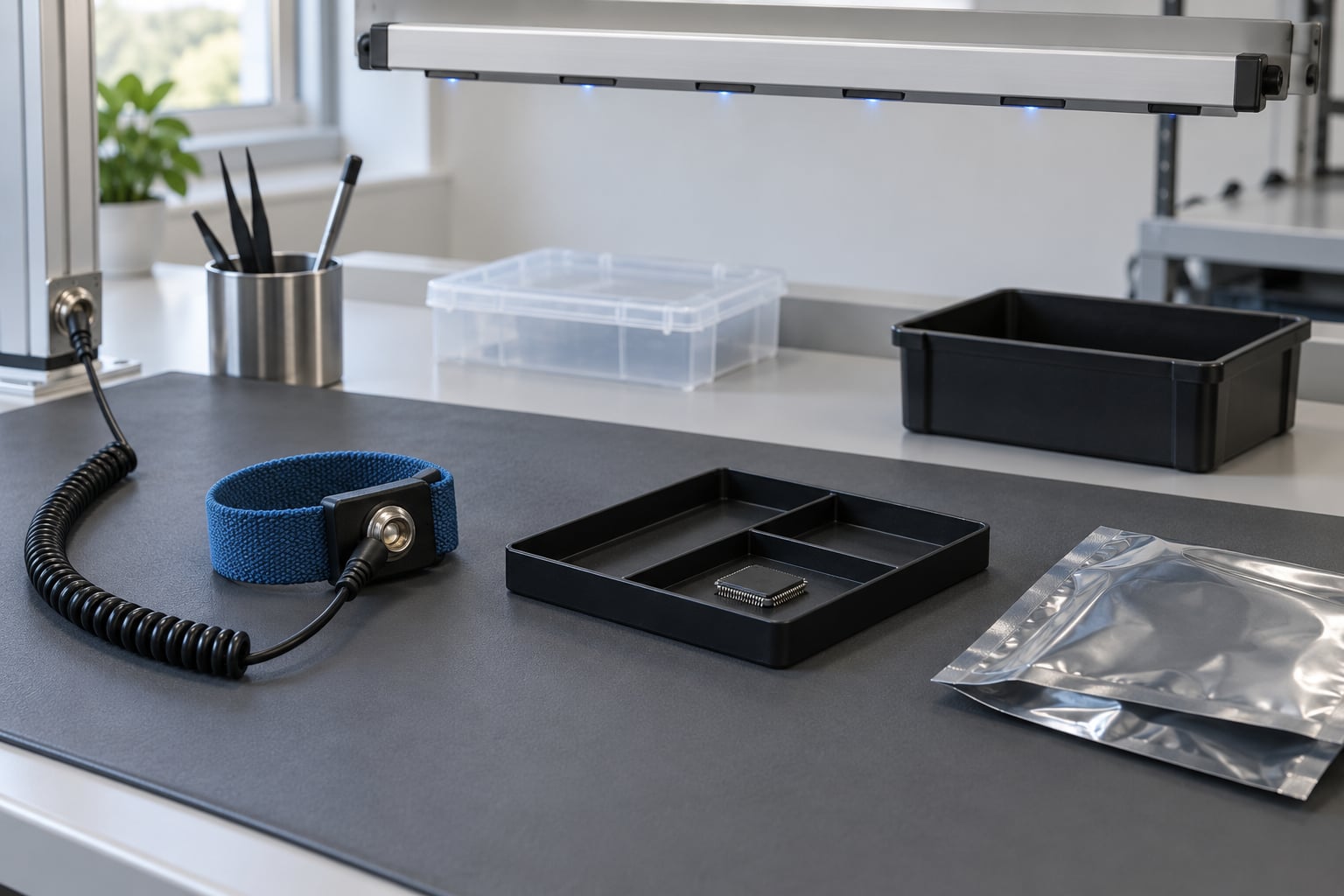
Antistatic handling of chips explained in plain terms: you ground yourself through a 1 MOhm-limited wrist strap, work on a dissipative mat, keep parts bagged until the last moment, and hold the room near 30-60% relative humidity. That is the whole discipline, and it takes about five seconds of setup.
What makes it worth doing is that the damage it prevents is usually invisible. A part that was zapped by static can pass incoming inspection, pass functional test, ship to a customer, and fail eight months later inside an assembly. This guide covers the physics briefly, then the bench procedure, for bare die, wafers, packaged ICs, leaded parts and assembled boards.
Table of Contents
- What Is Antistatic Handling of Chips and Why Does It Matter?
- ESD versus antistatic: the words are not interchangeable
- Why chips are uniquely vulnerable
- What actually cancels static electricity
- Catastrophic versus latent damage
- How Does Electrostatic Discharge Damage Semiconductor Devices?
- HBM, MM and CDM: the three damage models
- What Is the Correct Way to Handle Chips?
- How the rules change by part type
- How to check that your strap and mat actually work
- Which ESD Protection Equipment Should You Use?
- Myths worth retiring
- The standards to name
- How Do You Prevent Static When Receiving, Storing, and Shipping Chips?
- What to do after a suspected ESD event
- What Common Mistakes Can Damage Chips?
- Frequently Asked Questions
- Do all semiconductor chips need antistatic handling?
- What is the safest way to hold a bare IC or wafer die?
- Is an antistatic wrist strap enough to protect a chip?
- Can static damage be repaired after an electrostatic discharge event?
- How should chips be stored before and after soldering?
- Key Takeaways for Your Bench
What Is Antistatic Handling of Chips and Why Does It Matter?
Electrostatic discharge (ESD) is the sudden flow of a static charge between two objects at different voltages. On a bench it is not the spark you feel on a doorknob. It is a current pulse too fast to notice, entering or leaving a chip pin in nanoseconds, and it is the thing that kills integrated circuits.
Static charge builds on you constantly. Walking across a dry floor, sliding a chair, peeling a tape strip off a bench, even a cotton sleeve brushing against a board all separate surfaces that were touching, and the friction transfers charge between them. That transfer is called triboelectric charging. You then carry that charge to your bench, where it finds a path to ground through the first conductive thing it touches.
Prevention is the goal, damage control is what you do afterwards. A controlled work area, a verified ground path and disciplined part handling mean charge never accumulates in the first place. Damage control means recognising that a part was exposed, quarantining it, and getting it analysed before it reaches a customer.
ESD versus antistatic: the words are not interchangeable
People mix these up constantly, and the difference matters when you are reading a datasheet or a supplier’s handling instruction. “Antistatic” describes a material property. “ESD-safe” describes a system. An antistatic bag is useful on its own terms, but a bag does not protect the part once it is cut open with scissors and the lip is left lying against your bench.
| Term | What it actually means | Typical example |
|---|---|---|
| Antistatic | A material that does not generate or hold a large static charge; it dissipates slowly rather than instantly | Antistatic bag, antistatic mat, antistatic foam |
| Dissipative | Charge drains off over a controlled, measurable resistance and time rather than pooling | Bench mat rated in the 106 to 109 ohm range |
| Conductive | Low resistance, charge leaves almost immediately | Grounding point, conductive tote, ESD footwear |
| ESD-safe / ESD-protected | A complete system: grounded people, dissipative surfaces, ionizers, verified procedures | An electrostatic protected area (EPA) with a documented program |
| Insulative | Charge sits on the surface and stays there | Ordinary plastic bag, foam, vinyl, bubble wrap, plastic bins |
A part marked ESDS (ESD-sensitive device) is telling you it needs to be handled inside an EPA. The marking is not a warning label for shock risk to you. It is telling you the die cannot tolerate a fast transient.
Why chips are uniquely vulnerable
Most integrated circuits run on roughly 1 to 5 volts. A modern gate dielectric is on the order of a nanometre or two of oxide, and the electric field that field produces at 5 V already sits close to breakdown. Multiply that exposure by three orders of magnitude and you are puncturing the oxide or melting local metal interconnect.
The threshold for damage is well below what you can feel. Human perception of a spark starts around 3 kV at the fingertip, and you can carry charge far above that without noticing. A charged person touching a grounded pin is enough. So is a charged part touching a grounded fixture, a screwdriver tip, a tweezer, or the metal of a socket.
Devices that sit at the sharp end of the risk are the ones with thin dielectrics and high impedance: bare die, fine-pitch BGA and QFN parts, low-leakage analog and precision parts, RF devices, and any large-capacity die with a lot of surface to charge. Discrete power MOSFETs and older, thicker-oxide CMOS generally tolerate a casual touch better than most people assume.
What actually cancels static electricity
Three mechanisms do the work, and you need all three in a serious EPA.
- Grounding gives charge somewhere to go. Your wrist strap, the mat, the bench ground point and your footwear all tie you and the work surface to earth through a controlled resistance.
- Dissipation moves charge off surfaces slowly enough that no pulse forms. This is the job of the mat, the smock and the bags.
- Ionisation neutralises charge in the air itself, by putting balanced positive and negative ions into the airflow so any stray charge on an object is neutralised rather than waiting to discharge.
Humidity is the fourth, quieter factor. Above roughly 40% relative humidity, thin films of moisture on surfaces give charge somewhere to leak to. In a dry winter office or an air-conditioned lab, that path largely disappears and triboelectric charging gets much worse. Keeping the room between 30 and 60% relative humidity is the practical operating window; below about 30% you should expect trouble.
Catastrophic versus latent damage
ESD damage splits into two very different problems, and the second one is what makes static handling a quality issue rather than a hobbyist precaution.
| Type | What happens | How you find out | Typical timeline |
|---|---|---|---|
| Catastrophic | Oxide punctured, metal melted, junction shorted or opened, part is dead | Immediately, at test or at first power-up | Found on the bench or at final test |
| Latent | Silicon or oxide weakened, leakage path created, part still functions | Only at failure analysis, sometimes never | Months to years, often in the field |
Latent damage is the expensive one. A degraded part passes test, gets designed into a board, ships, and then fails in service where the real cost is a return, a teardown, a root-cause investigation and a field campaign across whatever has shipped since. Most ESD programs exist to protect against that second column.
How Does Electrostatic Discharge Damage Semiconductor Devices?
Two charging mechanisms produce almost every bench ESD event. Triboelectric charging is the rubbing one, already described. Electrostatic induction is the other: bring a charged object near a chip without touching it, and the field polarises the die and moves charge inside it. Ground the object and the accumulated charge flows to earth through the chip you never touched.
Induction is the reason “I did not touch it” is not a defence. A charged hand passing within a few centimetres of an exposed die can couple enough charge in to damage it.
The damage mechanism itself is usually dielectric or junction breakdown. Too much electric field across the thin gate oxide, or too much current through a PN junction, and the structure gives way. A chip also has on-die protection: power clamp and I/O protection devices designed to divert an ESD pulse to a rail. They help, and they have limits, and they are sized for the rated sensitivity of the part rather than for a large direct contact.
HBM, MM and CDM: the three damage models
Standards bodies model ESD events three ways so devices can be rated consistently. These are test models, not separate physical phenomena. Each has a mnemonic worth remembering.
| Model | Equivalent circuit | Rise time | Plain meaning |
|---|---|---|---|
| HBM – human body model | 100 pF in series with 1500 ohm | Around 60 ns | A charged person touches the pin |
| MM – machine model | 200 pF in series with 750 nH, no resistance | Around 10 to 20 ns | A charged metal tool or fixture contacts the pin – the harshest of the three |
| CDM – charged device model | Small capacitor in the package itself, typically sub-nanosecond | Under 1 ns | The chip is already charged and discharges outward, often by sliding a charged part across a surface |
HBM, MM, CDM: hand, machine, part. HBM is the one people picture, MM is the one that actually hurts, and CDM is the one people do not expect because nothing touched the pin.
JEDEC JS-001 and JS-002 define the human body and charged device test methods; the machine model was dropped from JEDEC qualification some years ago but still shows up in industry vocabulary and in failure analysis. Ratings are quoted per pin combination, since a device’s sensitivity to a signal pin differs from its sensitivity to a power rail.
TLP, or transmission line pulsing, is a different tool. Instead of a pass or fail rating, it produces a current-voltage curve for the protection structures, so an engineer can see trigger voltage, on-resistance and clamp behaviour. It is bench characterisation, not a qualification test, and it is how you compare two competing protection designs rather than two chips that are labelled sensitive.
What Is the Correct Way to Handle Chips?
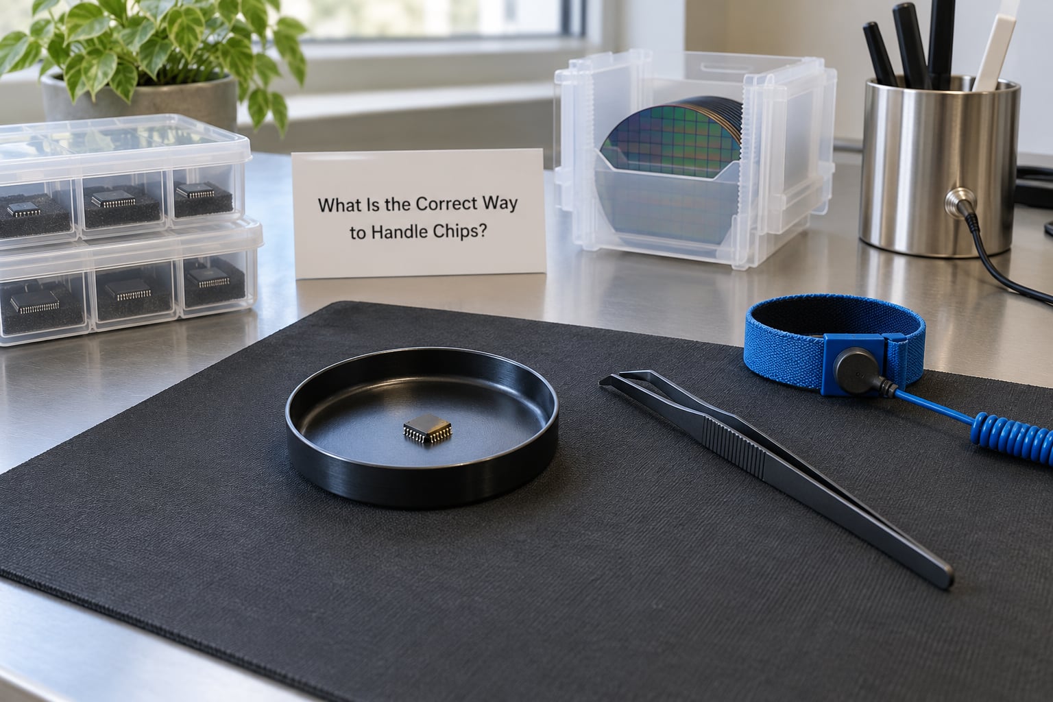
The sequence matters more than the equipment list. Grounding after you have already picked up a part is too late, because you are the charged object by then. Work in this order every time.
- Set up the area first. Mat down and connected to a verified ground point, ionizer on if there is one, humidity somewhere in the 30-60% band.
- Put the strap on and clip it before anything else. One wrist, snug, with the 1 MOhm limiting resistor in the lead. A bare ground wire with no resistor is a shock hazard and it is not a wrist strap.
- Verify the ground path. Test the strap and the mat before the first part of the day, not whenever you get around to it.
- Keep parts bagged. Do not lay loose components on the bench. Open the bag, take out what you need, and put the rest straight back.
- Never touch a lead, a pin or a die. Hold the package body or use a proper tool. If you can see the metal, treat it as off limits.
- Work with one hand on the mat at all times. If you need both hands on a part, use a fixture or a vacuum pickup rather than balancing the part on your free palm.
- Keep non-ESD items out of the area. Plastic bags, foam, vinyl, bubble wrap and personal items generate charge right where you are working.
- Repackage before you move. Back into the conductive container or bag before standing up, before crossing the room, before reaching for the phone.
How the rules change by part type
Bare die and loose ICs get the strictest treatment. Nothing gets picked up with fingers, ever. Use a vacuum pickup, a die pick or conductive tweezers, work over a grounded mat, and hold the die on a conductive foam block rather than a bench surface where it can pick up whatever charge the bench is carrying.
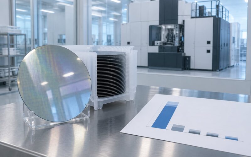
Wafers are handled at the edge with a dedicated wafer-handling tool, never at the centre where fingers leave oils and stress the crystal. A wafer carrier or a vacuum chuck that is properly grounded is better than any hand-held grip. Do not set a wafer face down on anything.
Packaged ICs in moulded bodies are the most forgiving, but the pins and any exposed thermal pad are still live conductors. Hold the body, watch for QFN and BGA parts with exposed pads and edge contacts, and keep the parts in their ESD-safe container until they are seated.
Leaded parts and connectors are where care is usually skipped because the part feels substantial. A through-hole DIP handled carelessly at the bench is still a chip lead. A resistor or a power diode is not usually at risk, but a low-leakage op-amp or a reference IC in the same bag is.
Assembled boards need the same discipline with a bit of nuance. A finished board with a hard ground plane and chassis connection is far less sensitive than a bare device, but the exposed connectors, test points and unpopulated footprints are not protected until they are covered.
How to check that your strap and mat actually work
Most straps that do not work are not broken; they are unverified. Cheap marketplace straps with no continuity through the coil, or a clip that never reached a real ground, produce no path at all and give false confidence.
Check it with a wrist strap continuity test meter, which verifies the strap and the ground system together rather than just the cord. A strap and grounding system that performs to ANSI/ESD S20.20 sits inside a defined resistance window from the wearer to ground. If you do not have a meter, at minimum confirm the cord reaches continuous metal, the clip seats firmly on a dedicated ground point, and the person wearing it can feel no shock from a low-energy source.
Mat verification needs its own instrument. A surface resistance meter confirms the mat is in the dissipative range and still connected to ground. A mat that has gone stiff, cracked or been wiped with a solvent-dominant cleaner can stop draining properly, and it will look perfectly fine doing it.
Which ESD Protection Equipment Should You Use?
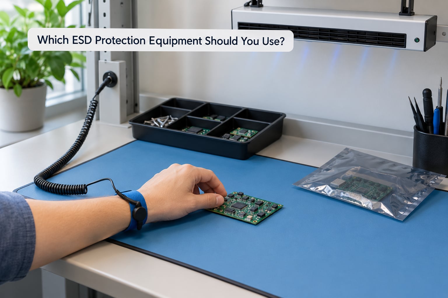
Here is what each item is for, and where it stops being enough. The common mistake is treating a list of equipment as a substitute for a program.
| Equipment | Purpose | Required? | Limitation |
|---|---|---|---|
| Grounding wrist strap with 1 MOhm resistor | Drains charge from the person, slowly enough to limit peak current | Yes, whenever you touch a bare device | One person only; does nothing for a chair or a tool on the bench |
| Dissipative bench mat | Drains charge from whatever is set on it | Yes, for any bench work | Wears out; only works while connected to ground |
| Grounded bench or ground point | The earth reference everything else hangs from | Yes | Needs periodic verification like any other item |
| ESD-safe bags, totes and conductive foam | Protects a part in transit between containers and the bench | Yes, for storage and transport | A bag cut open with scissors is no longer a bag; lose the seal and the protection |
| Ionizing bar or overhead ionizer | Neutralises charge in the air, covering shadows and ungrounded items | Recommended, essential for assembly lines | Never a replacement for grounding; needs cleaning and offset verification |
| Dissipative smock | Drains charge off clothing that would otherwise hold it | Recommended in production areas | Cotton and synthetic garments still generate charge; the smock manages it, it does not remove it |
| ESD footwear | Bonds the wearer to a grounded floor | Where the floor is the only ground path | Requires a proper conductive floor, not a rug |
| Gloves | Reduce direct contact with sensitive surfaces | Optional, and only as a supplement | Most gloves are not dissipative; a nitrile glove does not ground you |
| Humidity control | Keeps a leakage path on surfaces | Practical requirement | Needs monitoring, especially in winter |
Myths worth retiring
- “An ionizer replaces grounding.” It does not. Ionization removes charge from the air; grounding gives charge a path. Standards treat ionizers as a complement, never a substitute.
- “Wireless or no-screw straps work fine.” A strap with no reliable conductive path to earth is a decoration. There are certified wireless systems that use a coupling and grounding network, but a bare coin-cell strap with no ground connection does nothing.
- “Clipping to a PC case is fine.” Hobbyists do this and it is better than nothing, but a PC case is not a verified ground point. Use a dedicated earth stud or bench ground.
- “Cotton is safe, synthetic is dangerous.” Both generate charge. Cotton in dry conditions is a perfectly good charge generator, which is why the smock exists.
- “I did not feel a shock, so nothing happened.” The damaging pulses are far below human perception.
The standards to name
ANSI/ESD S20.20 defines an ESD control program covering facility, personnel, material and equipment requirements, and certification. IEC 61340-5-1 is its international counterpart for electronics manufacturing. JEDEC JS-001 and JS-002 define the human body and charged device qualification methods. If someone asks whether your setup is a real program rather than a mat and a strap, those three documents are the answer.
How Do You Prevent Static When Receiving, Storing, and Shipping Chips?
Most damage happens away from the bench, in the gap between the supplier’s dock and your mat. Packaging is the control that covers that gap.
Packaging. Parts ship in moisture barrier bags with a dry pack and desiccant, sealed and vacuum-packed. The bag is usually laminated conductive film, which is why it works: it dissipates rather than insulates. Follow the supplier’s handling instructions on the label, because they tell you the moisture sensitivity level, the floor life and the bake requirements.
Moisture sensitivity. An MSL rating is a time limit, not a formality. Once a sealed bag is opened, absorbed moisture starts coming out of the package. Exceed the floor life and the part can pop during reflow, with delamination and internal voids. Larger packages, wide BGA and lead-frame parts and many QFN devices are the most sensitive. If the floor life is exceeded, the part needs baking before reflow, not just a quick bake-and-ship.
Storage. Keep parts in their sealed bags, in conductive totes or shelving that does not accumulate charge, at the specified humidity, away from direct sunlight and away from any material that triboelectrically charges. Do not decant parts into ordinary plastic bins or onto an ungrounded shelf. Opening a bag early to count parts and then leaving it half closed is one of the most common ways good inventory gets damaged.
Incoming inspection. Inspect on a grounded, dissipative surface, in an EPA, wearing a strap. Do not open a bag and tip components onto a bench to count them. If you are checking moisture indicator cards, treat the card as a moisture device, not an ESD device.
Transport inside the building. A part in a bare anti-static bag is not protected in a cart that rolls over concrete and gets bumped. Use a conductive tote, keep the bag sealed or closed, and do not carry two loose bags in one hand while opening a third.
Shipping. The bag goes in a conductive tote, the tote gets a label that names the ESD sensitivity, and the whole thing is packed so nothing shifts. Carrier and courier requirements matter here, and so does the record: the packaging choice is often the only evidence you have if a shipment arrives damaged.
SMT and pick-and-place. In an assembly line, feeder and carrier tape handling is an ESD event waiting to happen. Anti-static carrier tape, grounded feeders, an ionizing bar over the placement head, and grounded load boards and sockets in the test handler are the controls. The machine model is a machine problem, and it is the reason the 750 nH in that equivalent circuit exists.
What to do after a suspected ESD event
If you think a part was exposed, treat it as suspect rather than as probably fine. Remove it and everything that was near it from the flow. Bag them separately, label them with the date, the bench, the operator and the suspected mechanism, and do not put them back into inventory.
Then get them to failure analysis. ESD damage is often identifiable from the failure signature and from the physical evidence at the pin, where a melted crater or a punctured dielectric tells the story. Keeping that quarantined sample, with its paperwork, is what lets an engineer confirm the mechanism instead of guessing. Guessing is how a real ESD problem gets attributed to the wrong cause and never gets fixed.
What Common Mistakes Can Damage Chips?
Almost every bench ESD event traces back to one of these. Each has a simple correction.
- Unplugging grounded equipment mid-task. The instant the ground path is broken, you become the charged object in the room. Fix: leave grounded equipment connected, or disconnect it before you touch it and reconnect after.
- Touching leads, pins or exposed pads. Fix: hold the package body. If the body is not graspable, the part needs a tool.
- Using ordinary plastic bins, foam or bubble wrap. All of it is insulative. Fix: conductive totes, anti-static bags, conductive foam.
- Laying bare parts on an ungrounded bench. Fix: keep parts in the container until the mat is down and you are grounded.
- Skipping the 1 MOhm limiting resistor. A direct ground wire limits nothing and is a shock hazard. Fix: use a proper strap.
- Assuming a grounded case is enough. A grounded metal enclosure tells you nothing about charge on the parts inside it. Fix: strap, mat and procedure, not a substitute.
- Never verifying the strap. A broken coil, a loose clip or a missing earth stud all produce silence and no protection. Fix: test it on a schedule and at the start of each day.
- Reaching for a non-conductive tool. A plastic-handled screwdriver and a nylon tweezer are charge carriers. Fix: conductive or dissipative tools with defined specs.
- Leaving cut bags and packaging on the bench. Fix: put packaging in the bin it belongs in, immediately.
- Working at low humidity and blaming the equipment. A dry room makes every other control work harder. Fix: monitor relative humidity and keep it in the 30-60% band.
Frequently Asked Questions
Do all semiconductor chips need antistatic handling?
Every part benefits, but the risk is not uniform. Moulded-package parts with thick gate oxides and discrete power devices usually survive a casual touch. Bare die, fine-pitch BGA and QFN, low-leakage analog, precision references, RF parts and any large die with thin dielectrics genuinely need ESD-safe handling. The practical rule in a lab is to treat everything marked ESDS as protected, because the cost of guessing wrong is a latent failure in the field.
What is the safest way to hold a bare IC or wafer die?
Use a vacuum pickup, a die pick or a pair of conductive tweezers, and hold the die on conductive foam or a grounded surface rather than a bench. For wafers, grip only the edge with a dedicated wafer-handling tool. Never touch a die face or a lead with skin, and keep the part in a conductive container whenever it is not actively in use at a grounded station.
Is an antistatic wrist strap enough to protect a chip?
On its own, no. A correctly fitted strap with a 1 MOhm limiting resistor drains charge from you, but it does nothing for charge on the bench, on a tool, on a chair or in the air. A working station needs a dissipative mat connected to a verified ground point, ESD-safe containers, and an ionizer in high-traffic areas. The strap is the part most likely to be missing from a broken setup, not the part that replaces the rest.
Can static damage be repaired after an electrostatic discharge event?
Almost never. A catastrophically damaged die cannot be revived, because the failure is physical oxide breakdown or melted metal. Latent damage is worse in one way and better in another: the part still works, but you cannot tell whether it is sound. The only useful action is to quarantine the suspect parts, document the suspected mechanism, and have them analysed. There is no bench procedure that makes a zapped part trustworthy again.
How should chips be stored before and after soldering?
Before soldering, keep parts sealed in their moisture barrier bags with the dry pack and desiccant intact, in conductive totes or shelving, within the specified humidity and within the floor life printed on the bag. Opening a bag starts that clock. After soldering, the residual concern shifts from ESD to moisture and mechanical stress, so let boards dry fully before conformal coating, keep them off insulating surfaces that block drainage, and follow the supplier’s bake requirements if the floor life was exceeded.
Key Takeaways for Your Bench
Start with the ground. Fit a wrist strap with a 1 MOhm limiting resistor, put a dissipative mat on a verified ground point, and check both before you open a single bag. Then work in order: grounded first, part out of its container last, back in the container before you stand up.
Keep relative humidity near 30-60%, treat ionizers as a complement rather than a substitute for grounding, and stop reaching for plastic boxes, unverified straps and tools with plastic handles. If something does get exposed, quarantine it and get it analysed. The whole point of antistatic handling of chips is that the failures you cannot see cost far more than the ones you can.