Transistor biasing is the process of applying DC voltages and currents to a transistor so that it sits at a chosen operating point, called the Q-point, in its active region before any signal arrives. Get that resting point right and the transistor amplifies cleanly; get it wrong and the output clips, drifts with temperature, or runs away. Here is how the idea works, how the common bias circuits differ, and how to design and check one from real numbers.
Beginners usually meet biasing as a formula to memorise. Transistor biasing basics explained is more useful as a set of physical decisions: how much current do you want through the collector, how much voltage should be left across the transistor, and what keeps those two numbers steady as the part warms up.
Table of Contents
- What Is Transistor Biasing?
- Why the Q-Point Matters
- How DC Biasing Differs from Signal Operation
- Transistor Biasing Basics: The Operating Point
- Common BJT Biasing Methods
- Why the Q-Point Drifts: Thermal Stability and Runaway
- How MOSFETs Are Biased
- A Step-by-Step Design Example
- Common Biasing Mistakes and How to Fix Them
- How to Verify the Bias Point
- Frequently Asked Questions
- What is transistor biasing in simple words?
- How do you properly bias a transistor?
- What is the most common way to bias a transistor?
- What are VBB and VCC in transistors?
- What causes thermal runaway in a transistor?
- How do MOSFETs differ from BJTs in biasing?
- Conclusion
What Is Transistor Biasing?
Biasing means setting the DC conditions of a transistor with a resistor network. Those conditions are a base-emitter voltage, a base current, a collector current and a collector-emitter voltage, and the network exists to hold them at chosen values.
Consider a small common-emitter stage. The input signal swings the base voltage up and down by a few millivolts, and because the base-emitter junction responds to voltage, the collector current follows those swings. The stage has no output at all with no input unless the transistor is already switched on and sitting in the right region, which is what the bias network arranges.
So biasing and signal operation are two different jobs sharing one device. The bias network sets the DC starting condition; the signal pushes the device back and forth around that condition.
Why the Q-Point Matters
The Q-point is the DC operating point of the transistor, and the Q stands for quiescent, meaning the transistor is at rest with no input signal applied. Designers place it near the middle of the DC load line so the output can swing in both directions before it hits a limit.
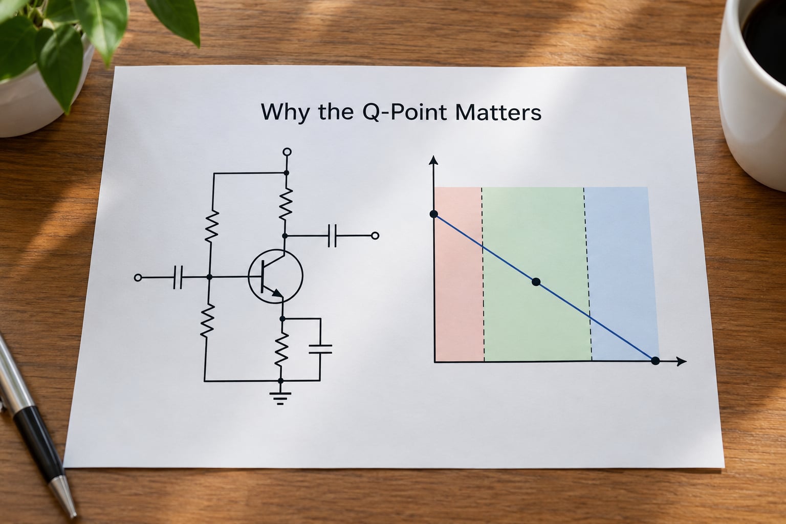
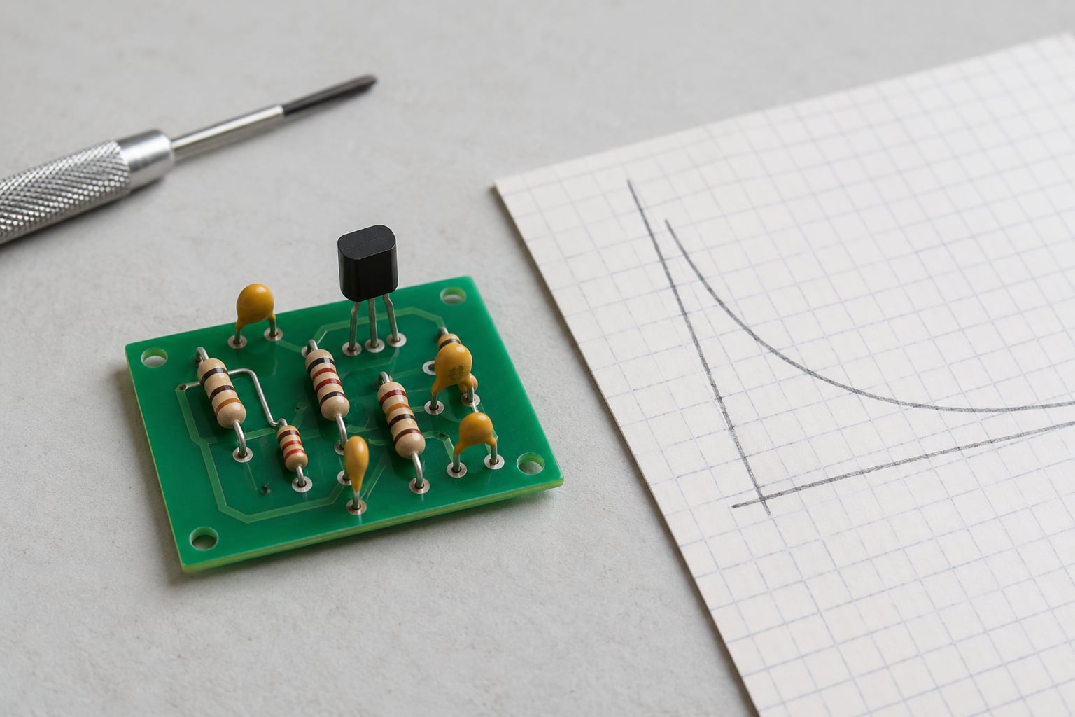
The load line itself comes straight from the DC circuit. With a collector resistor RC and no emitter resistor, Ohm’s law along the collector loop gives VCE = VCC minus IC times RC, so the allowed combinations of IC and VCE fall on a straight line between the two extremes: IC = 0 at VCE = VCC, and VCE = 0 at IC = VCC over RC. Everything in transistor biasing basics explained downstream, from the divider values to the stability factor, starts with where you sit on that line.
| Region | Base-emitter junction | Collector-base junction | What you see at the output |
|---|---|---|---|
| Cutoff | Reverse biased | Reverse biased | Flat tops, small signals on one side only |
| Active | Forward biased | Reverse biased | Clean symmetric amplification |
| Saturation | Forward biased | Forward biased | Flattened bottoms, heavy current, possible damage |
Two failure modes show up in every beginner build. Bias too close to cutoff and the positive peaks of the input run the transistor out of active region, which sounds like a thin, hollow distortion. Bias too close to saturation and the negative peaks flatten out instead, and the transistor carries more current than the signal needs.
Placing the Q-point at the middle of the load line gives the largest undistorted swing in either direction. That is the whole reason the load line is drawn, even though most working designs just check the numbers afterwards.
Two numbers define the limits of that line. The knee voltage VCE(sat) is the collector-emitter voltage at which the transistor stops behaving like a current source and simply becomes a closed switch, typically a fraction of a volt for a silicon part. The other limit is the maximum collector current set by RC and by the device rating, usually far above where you would ever put the Q-point.
Adding an emitter resistor changes the picture slightly and is worth understanding early. For AC, the emitter is bypassed and the emitter resistor does not appear in the AC load line, so the line runs from roughly VCC to the knee voltage. For DC the emitter sits above ground, so the DC load line is flatter, spanning VCC minus VE down to about VE plus a fraction of a volt. Many textbooks call these the AC and DC load lines, and the Q-point has to sit inside both of them, not just the DC one.
How DC Biasing Differs from Signal Operation
In DC analysis you ignore the signal source and the coupling capacitors, because a capacitor blocks steady DC and an AC source set to zero volts looks like a short to ground. What remains is the bias network and the supply, and that gives you the Q-point.
In AC analysis you set the DC supply to zero volts, which turns it into a short, and now the coupling and bypass capacitors matter. The small-signal version of the circuit has no large currents, and the gain is set by the surrounding resistors and the device’s transconductance rather than by the Q-point directly.
The link between the two is the available signal swing. A transistor sitting at the middle of the load line has roughly the same headroom toward cutoff as toward saturation, so the largest input that stays in the active region is roughly twice what it would be with the Q-point parked near one end.
Transistor Biasing Basics: The Operating Point
A handful of quantities describe the operating point, and it pays to know them in this order. First the supply voltage VCC, the single rail that powers the stage. Then the base-emitter voltage VBE, which sits around 0.6 to 0.7 V for a silicon transistor and is not set by you directly.
Next come the currents. Base current IB flows into the base terminal, and collector current IC flows out of the collector. In the active region the two are related by IC = beta times IB, where beta is the common-emitter current gain and varies far more than most datasheet tables suggest.
Finally the voltages across the device. Collector-emitter voltage VCE is what is left of the supply after the collector resistor and any emitter resistor have taken their share. Together IC and VCE define the Q-point on the load line.
Two approximations make hand calculation workable. Neglecting base current gives emitter current as roughly equal to collector current, and treating VBE as a fixed 0.7 V. Both are fine for a first design pass and both are worth checking once the real part is in the circuit.
One more parameter deserves a mention early because it causes most of the surprises: leakage current ICBO, the collector-to-base leakage with the emitter open. It is tiny at room temperature but roughly doubles for every 10 degree Celsius rise, and it is the seed of thermal runaway.
That last pair is why the input signal stays small in millivolts rather than volts. A base-emitter junction is a diode, and a diode’s incremental resistance at 1 mA is on the order of 25 ohms, so a 10 millivolt input moves roughly 0.4 milliamps of junction current, and the transistor multiplies that by beta. That multiplication is the whole trick, and it only works while the stage stays inside the active region.
Common BJT Biasing Methods
Four arrangements cover most discrete work, and they differ mainly in how much they resist the things that move: beta variation, temperature and supply drift.
Fixed base bias connects a single resistor RB from the supply to the base. The current is IB = (VCC minus VBE) over RB, and since IC depends directly on beta, a part with beta 100 lands somewhere completely different from one with beta 300 of the same part number. It is simple enough to describe in one line and unstable enough that hobbyists usually end up abandoning it after the first hot afternoon.
Collector feedback bias returns a fraction of the collector voltage to the base through one resistor. If collector current tries to rise, VCE falls, the base gets less drive, and the current backs off. That negative feedback is what makes the arrangement work, and its weakness is the feedback ratio depends on the transistor, not on resistors you chose.
Voltage divider bias puts two resistors, R1 from the supply to the base and R2 from the base to ground, and adds an emitter resistor RE. This is the arrangement almost every analog designer reaches for first, including most of the people posting on electronics forums who will tell you that in real design you go straight here.
The divider can be analysed two ways. The approximate method ignores base current, so VB = VCC times R2 over (R1 + R2), VE = VB minus VBE, and IE = VE over RE. The exact method replaces the divider with its Thevenin equivalent: VTH = VCC times R2 over (R1 + R2) and RTH = R1 in parallel with R2, then IB = (VTH minus VBE) over (RTH plus (beta + 1) times RE).
Emitter degeneration is really a modifier rather than a separate method. Adding RE in the emitter gives the strongest of the stabilising effects, because current that tries to rise also raises the emitter voltage and cuts the base-emitter drive. The cost is gain: without a capacitor across RE, the emitter resistance sits in the AC path too and reduces voltage gain.
| Method | Stability | Sensitive to beta | Component count | Typical use |
|---|---|---|---|---|
| Fixed base | Poor | Severely | Two resistors | Teaching, switch-like circuits |
| Collector feedback | Fair | Moderately | Two resistors | Simple low-cost stages |
| Voltage divider with RE | Good | Slightly, if the divider is stiff | Three resistors | Most general-purpose amplifiers |
| Emitter degeneration alone | Good | Strongly, but predictably | Base drive plus RE | Current-source-like stages, power output |
Whether a divider is stiff depends on how much current it supplies compared with the base current it has to feed. The common rule of thumb is that divider current should be roughly ten times base current; some designers use five, some use twenty, and the difference is the trade between wasted supply current and a divider that gets dragged around by base current. When the divider current is at least ten times IB, base current has a small effect and the exact calculation is barely different from the approximate one.
Voltage divider bias sits at the useful end of the range. Stability is good and it does not depend on a feedback ratio that changes with the transistor, which is why the stability factor, defined as the change in collector current per change in leakage current, is low compared with fixed bias.
Why the Q-Point Drifts: Thermal Stability and Runaway
Every bias network loses ground over temperature, and the two dominant mechanisms pull in the same unhelpful direction. Base-emitter voltage falls by roughly 2 mV for every degree Celsius, so a transistor held at a fixed base voltage asks for more current as it warms. Leakage current rises at the same time, roughly doubling every 10 degrees Celsius, adding to collector current on top of that.
More collector current means more heat in the device, which means a higher junction temperature, which means more current still. That loop is thermal runaway, and once the gain of the loop exceeds unity it does not stop on its own.
Prevention works by making one of the links in that loop negative. The cheapest is the emitter resistor, because a rise in emitter current raises VE, which reduces VBE, which reduces the current. If that is not enough, put a forward-biased diode, or a VBE-matched pair, in the base or emitter path; its forward voltage falls at the same 2 mV per degree as the transistor’s, so it holds the junction voltage roughly constant.
A thermistor with the right negative temperature coefficient in the emitter path is the third option, and it lets you trim the compensation point rather than accept whatever the diode gives you. For a first amplifier, resistor alone is normal. For a power output stage pushing close to the device current rating, use a thermistor or a matched diode and check the design with a temperature sweep, because compensation that works at 25 degrees can be wrong at both ends of the range.
There is a second temperature effect that is not a runaway at all, and it is worth separating. Beta rises with temperature as well, so a fixed base-current bias pushes the Q-point upward as the part warms even before leakage matters. That is a slow drift rather than a runaway, and a stiff divider plus an emitter resistor removes most of it. Plotting collector current against temperature across the full range tells you which of the two you are dealing with.
How MOSFETs Are Biased
A MOSFET is biased by voltage rather than current, which changes both the design and the failure modes. An enhancement-mode NMOS conducts once the gate-source voltage VGS passes the threshold voltage VTH, typically a volt or two for a logic device and three to five for a power part. Below that the device is off.
For a common-source stage you set VGS with a divider, R1 from supply to gate and R2 from gate to ground, so VGS = VDD times R2 over (R1 + R2). Add a source resistor for stability the same way you would on a BJT, and the gate draws essentially no DC current, so the divider is not loaded at all. That is a genuine practical advantage over bipolar dividers.
Drain feedback works on the same principle as its bipolar counterpart: a resistor from drain to gate lowers VGS when drain current rises. A PMOS version simply inverts the polarities, with the divider referencing VDD downward and the source typically tied to the supply.
A current-source bias, often a resistor in the source with a fixed gate voltage or an active current mirror in an integrated design, sets the drain current almost independently of the device. It holds current well but needs headroom, and it is where the cascode arrangement gets its voltage swing.
The difficult part of MOSFET biasing is threshold voltage spread. VTH varies several volts between parts of the same part number, and it also shifts with temperature and with body effect. Design for the worst case: pick a gate voltage a volt or two above the highest expected VTH if you need the device to stay in saturation, and accept that some parts will sit lower on the transfer curve.
Where BJT biasing leans on beta, MOSFET biasing leans on that VTH spread plus the transconductance, which is set by the drain current you chose. Everything else in the layout is the same story: resistors from a supply, a target operating point, and a check that the real part lands where you designed it.
A Step-by-Step Design Example
Transistor biasing basics explained in practice is easier with one complete worked case, with every assumed value labelled so you can swap the numbers for your own. Supply VCC = 12 V. Target collector current IC = 1 mA. Target collector-emitter voltage VCE = 6 V, roughly the middle of a 0 to 12 V span. Assumed beta = 150. Assumed VBE = 0.7 V.
Step one is the collector resistor. The voltage dropped across RC is the supply minus VCE, so RC = (12 minus 6) over 1 mA = 6 kilohms. Step two is the emitter resistor. Emitter current is close to 1 mA, and we choose an emitter voltage of about 2.2 V, so RE = 2.2 V over 1 mA = 2.2 kilohms.
Step three is the base voltage. VB = VE plus VBE = 2.2 plus 0.7 = 2.9 V. Step four is the divider. We want divider current of about ten times base current; base current is 1 mA over 150, which is 6.7 microamps, so 67 microamps is the target. With R2 carrying roughly that current, R2 = 2.9 V over 67 microamps is about 43 kilohms, and picking the standard 47 kilohm value gives R1 = (12 minus 2.9) over 67 microamps, about 136 kilohms, so 150 kilohms is the nearest common value.
| Quantity | Assumed or chosen | Result |
|---|---|---|
| Supply VCC | Given | 12 V |
| Target IC | Given | 1 mA |
| Target VCE | Given | 6 V |
| Beta | Assumed | 150 |
| RC | Calculated | 6 kOhm |
| RE | Calculated | 2.2 kOhm |
| VB | Calculated | 2.9 V |
| R1 | Chosen standard value | 150 kOhm |
| R2 | Chosen standard value | 47 kOhm |
Step five is checking the result rather than trusting it. With 150 kOhm and 47 kOhm the Thevenin voltage is 12 times 47 over 197, which is 2.86 V, and the Thevenin resistance is 150 in parallel with 47, about 35.7 kOhm. That gives IB = (2.86 minus 0.7) over (35.7 kOhm plus 151 times 2.2 kOhm) = 2.16 over 367.9 kilohms, which is 5.9 microamps, and IC = beta times IB is about 0.88 mA. That is close to the 1 mA target, and the exact method wins over the approximate one.
The reason is visible in the numbers. 151 times 2.2 kilohms is 332 kilohms, which dwarfs a Thevenin resistance of only 35.7 kilohms, so the emitter branch dominates the calculation and beta no longer fully cancels. An emitter resistor of that size needs a much stiffer divider, and the ten-times rule above was sized against the base current of the intended design rather than the one that actually appears.
So the design needs a second pass, and the fix is a stiffer divider. Keep RE at 2.2 kilohms and raise the divider current until the emitter branch stops dominating: at 300 microamps, R2 = 2.9 V over 300 microamps is about 10 kilohms and R1 = 9.1 V over 300 microamps is about 30 kilohms. Recalculate with those standard values and the Thevenin voltage becomes 12 times 10 over 40, which is 3.0 V, with a Thevenin resistance of 30 in parallel with 10, or 7.5 kilohms.
Now IB = (3.0 minus 0.7) over (7.5 kOhm plus 151 times 2.2 kOhm) = 2.3 over 339.7 kilohms, which is 6.8 microamps, and IC = 150 times that is 1.02 mA. That lands on the target. The lesson is that the ten-times rule needs headroom when RE is large, because the base current it was sized against is the one the divider has to supply before the emitter resistor takes its share.
Step six is power. At 1 mA, RC dissipates 6 milliwatts, RE dissipates a little over 2 milliwatts, and the transistor itself dissipates VCE times IC, roughly 6 milliwatts at the target point. Quarter-watt resistors and a small TO-92 package with a little copper are comfortable; the numbers are worth writing down anyway, because they are what tell you when a bias design needs a heat sink instead of a printed circuit board trace.
Step seven is verification. Enter the circuit in a simulator, run a DC operating point analysis, and read the node voltages. If the simulated collector voltage sits near 6 V, the design is close. If it sits near 0 V, the device is in saturation; if it sits near 12 V, the device is barely on. Simulation alone is not enough, because the model carries a typical beta and typical VBE, which is exactly the assumption that fails in the real world.
The general lesson is worth stating plainly. The result above is not a universal answer, because it assumed a beta of 150 and a VBE of 0.7 V, and real parts scatter around both. What survives the part-to-part spread is the method: pick the Q-point, pick the resistors, calculate, then measure.
A note on choosing VBE. The common shortcut fixes it at 0.7 V, which is optimistic for a silicon part carrying around 1 mA. Where a little more accuracy matters, subtracting 0.6 V or using the 0.6 to 0.7 V band and testing both ends costs nothing. The KVL equation for the emitter loop, VCC equals IC times RC plus IE times RE plus VBE plus VCE, is the one to keep on the bench, because every bias method is a rearrangement of it.
Internal emitter resistance, usually written rEE, deserves a mention because textbooks skip it and small designs feel it. It is the dynamic resistance of the emitter-base junction, roughly 25 millivolts over IC, so 25 ohms at 1 mA. If your calculated RE is only tens of ohms, rEE is a significant fraction of it and the current comes out lower than you predicted. Either design RE well above rEE, or include rEE in the calculation and treat it as part of the total emitter resistance.
Lastly, check the load. The bias network decides the Q-point, but the collector resistor and whatever sits after the coupling capacitor also determine the AC load line. A 10 kilohm load resistor on a stage with a 6 kilohm RC will cut the voltage gain noticeably, and in some designs the Q-point that looked correct on the DC calculation is not the point that gives the most clean output swing. Simulate with the real load attached, not with an ideal open circuit.
Common Biasing Mistakes and How to Fix Them

Ignoring base current. A divider sized so the base draws a noticeable fraction of the divider current will not hold the base voltage you calculated. Fix: use the exact Thevenin method, or size the divider for at least ten times the base current and stay on the approximate method.
Sitting too close to a boundary. A Q-point at 0.5 V of VCE looks fine on the schematic and clips badly on the bench. Fix: aim for the middle of the load line, and if the signal is large, aim for a little more than half the supply so the swing stays inside the region.
Overlooking resistor power ratings. Bias resistors in a low-current signal stage dissipate milliwatts, so a 1/4 watt part is plenty. The same calculation on a driver or output stage reaches watts. Fix: multiply current squared by resistance for each resistor and compare with the rating before layout, not after a failure.
Leaving out the emitter resistor. A divider alone sets the base voltage but nothing limits current when temperature rises or beta climbs. Fix: add RE, and treat it as part of the bias design rather than an optional extra.
Assuming a beta that does not exist. Parts sold under one part number commonly span beta 100 to 300, and the same transistor can differ by a factor of two between suppliers. Fix: design the bias so the Q-point barely moves when beta doubles, which means either a stiff divider or a meaningful RE.
Forgetting temperature. VBE falls by roughly 2 mV per degree Celsius while ICBO rises, so an unsheltered stage walks uphill as it heats. Fix: RE for the gain trade, a VBE-matched diode or thermistor in the base path for tighter work, and adequate copper or a heat sink on the device itself.
How to Verify the Bias Point
Start with a DC operating point analysis in simulation and read the collector and emitter node voltages. Those two numbers, with the supply, tell you immediately which region the device is in. A collector voltage within a volt or two of the supply means the transistor is off or barely on; a collector voltage close to the emitter voltage means it is in saturation.
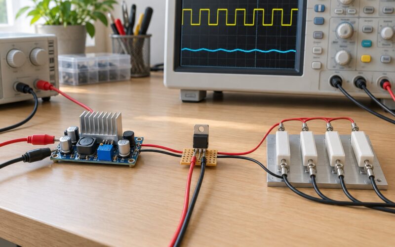
On the bench, a multimeter in DC voltage mode across the collector resistor gives the voltage drop, and dividing by the resistance gives the actual collector current. Measuring across the emitter resistor gives emitter current the same way. Because the meter input impedance is high, these readings are close to the true circuit values at DC, where no signal is moving.
Sweep the supply next. Run it from about 80 percent to 120 percent of nominal and watch the collector voltage. A stiff bias holds roughly in place; fixed base bias moves a long way, which is exactly the behaviour that turns a warm afternoon into a broken transistor.
Sweep temperature in simulation across the full commercial range, for example minus 40 to plus 85 degrees Celsius, and plot collector current against temperature. The design is thermally acceptable if current falls or stays roughly flat as temperature rises. Any design where current climbs steeply with temperature is a thermal runaway candidate.
Signs of a wrong operating point are recognisable without instruments. A stage that distorts on quiet passages and recovers on louder ones is often biased too low. A stage that gets hot, current climbs, or the output collapses into a dull roar is a runaway signature. A stage whose output sits near half the supply in silence and clips at both extremes is a coupling or load problem, not a bias problem.
Frequency belongs in the check too, because the bypass capacitor across RE shapes the low end. The rule of thumb is to make the capacitor reactance at the lowest frequency of interest no more than a tenth of RE, so for 20 Hz and a 2.2 kilohm emitter resistor, 47 microfarads is a reasonable starting point. Too small a value and the gain rolls off audibly at the bottom; too large and nothing much changes, apart from the part count.
The stability factor completes the picture. It measures how much collector current moves for a given change in leakage current, and it falls as the bias circuit gets better. Fixed bias has a large factor and a badly behaved Q-point, while divider bias with a stiff divider and a real RE has a small one.
Frequently Asked Questions
What is transistor biasing in simple words?
Transistor biasing is setting the DC voltage and current conditions of a transistor so it rests at a chosen operating point, the Q-point, in its active region before any signal arrives. A resistor network from the supply applies a base voltage and current, which produce a collector current and a collector-emitter voltage. The aim is symmetrical signal swing with no clipping and a Q-point that stays put as temperature and beta change.
How do you properly bias a transistor?
Decide the Q-point first, usually about half the supply across the transistor, then choose the base voltage, emitter voltage and currents around it. Add an emitter resistor for stability, and size the base divider so it supplies roughly ten times the base current. Calculate with the Thevenin equivalent of the divider, then check the collector voltage in simulation and on the bench before the amplifier goes into a case.
What is the most common way to bias a transistor?
Voltage divider bias with an emitter resistor is the most common method in discrete analog work. Two resistors set the base voltage and RE develops most of the DC voltage, which makes the operating point depend far more on the supply than on the transistor’s beta. The divider current is usually set at about ten times the base current so that base current barely moves the base voltage.
What are VBB and VCC in transistors?
VCC is the supply rail that provides the DC power to the circuit, usually the single positive supply in a single-supply design. VBB is the base supply, the DC voltage that forward biases the base-emitter junction and sets the base current. In a single-supply circuit VBB is often derived from VCC through a divider, so the two are linked rather than being separate sources.
What causes thermal runaway in a transistor?
Thermal runaway is a positive feedback loop. As a transistor heats, base-emitter voltage falls by roughly 2 mV per degree Celsius and leakage current rises, so collector current increases, which dissipates more power, which heats the device further. A negatively temperature-compensated element in the emitter or base path, such as a resistor or a matched diode, counteracts it. Small-signal stages rarely run away; power output stages do.
How do MOSFETs differ from BJTs in biasing?
A MOSFET is biased by gate-source voltage rather than base current, and the gate draws almost no DC current, so a gate divider is not loaded the way a bipolar divider is. The complication is threshold voltage spread: VTH can vary several volts between parts of the same part number and shifts with temperature and body effect. BJT designs worry about beta, MOSFET designs worry about VTH variation and the transconductance it sets.
Conclusion
The first practical step in any bias design is choosing the Q-point, because every resistor value follows from it. Pick the collector current and the collector-emitter voltage you actually want, work back through the emitter resistor and the base divider, then measure the collector voltage on the real board.
That is transistor biasing basics explained in one line: set the operating point first and let the resistor values follow it. Do not choose resistor values in isolation and hope the transistor lands in the right region. The parts scatter, the temperature moves, and a circuit that only works on the bench at 22 degrees Celsius is not finished.