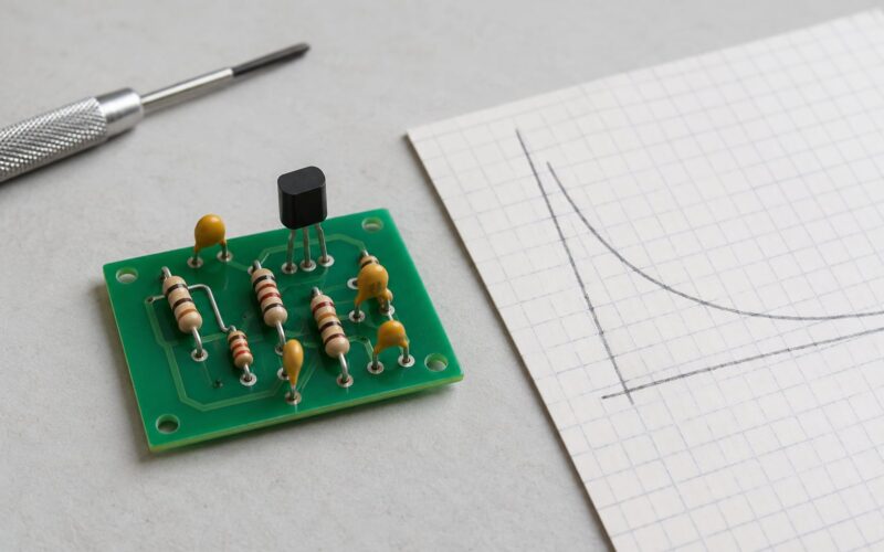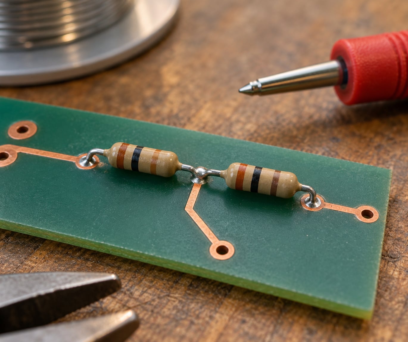
A voltage divider is two resistors in series across a supply, with the output taken from the junction between them, and the output voltage is the input voltage multiplied by the ratio of the bottom resistor to the total series resistance. That is the whole idea. Getting voltage divider design right comes down to picking values that hit your target ratio, staying accurate once something real is attached to the output, and keeping each resistor under its power rating.
This guide walks from requirements to a finished, verified circuit. Every example shows the arithmetic, not just the final number, because the number that matters is usually the one after you round to a value that actually exists in the E24 or E96 table.
Table of Contents
- What Is a Voltage Divider?
- Voltage Divider Formula and How It Works
- Ratios worth memorising
- Rearranging the formula
- Voltage Divider Design Step by Step
- The seven-step design procedure
- Verify it on the bench
- How to Choose Resistor Values
- Standard values and how the rounding error works
- Why smaller values are usually better
- Which tolerance do you actually need
- Loading Effects and Output Impedance
- The 10x loading rule
- Buffering the output
- Power Rating and Resistor Safety
- Common Voltage Divider Design Examples
- Scaling a 12 V battery to a 3.3 V ADC input
- Shifting a 5 V logic signal down to 3.3 V
- Reading a thermistor with a microcontroller
- Biasing an NPN transistor
- Measuring a 48 V bus safely
- How to Improve Divider Accuracy
- Ratio tolerance instead of absolute tolerance
- Buffering and the ADC front end
- Noise, leakage and layout
- When a divider is the wrong tool
- Troubleshooting the symptoms people actually hit
- A short checklist before you solder
- Frequently Asked Questions
- What is the minimum resistance I should use in a voltage divider?
- Can a capacitor be connected to the output of a voltage divider?
- How do I calculate the power rating of divider resistors?
- Why does my divider output change when I connect a load?
- When should I use an op-amp buffer after a voltage divider?
- What is the 10% rule for voltage dividers?
- Conclusion
What Is a Voltage Divider?
A voltage divider is a passive network of two or more resistors connected in series across a voltage source. The output is taken at the node between them, relative to ground, and it is always a fraction of the input voltage.
      Vin
       |
      R1          (top resistor, "high side")
       |
       +---- Vout <-- output taken here
       |
      R2          (bottom resistor, "low side")
       |
      GND
The two resistors are usually labelled R1 for the upper one and R2 for the lower one. Because the same current flows through both of them, the voltage splits in proportion to resistance, and each resistor takes a share of the supply proportional to its size.
Where dividers show up in real boards:
- Scaling a higher voltage down into the input range of an analog-to-digital converter.
- Sensing a resistive sensor, where a thermistor, light-dependent resistor or strain gauge changes resistance and the divider turns that into a voltage a microcontroller can read.
- Biasing a transistor, setting the base voltage that fixes the operating point.
- Generating a reference from a supply when a fixed reference voltage is all you need.
- Level shifting a 5 V logic signal down to a 3.3 V input without a translator chip.
It is two components and no active devices, which is exactly why it is everywhere, and also why it has a hard limit: a divider cannot supply current. Everything that follows is either about hitting the ratio precisely or about dealing with that limit.
Voltage Divider Formula and How It Works
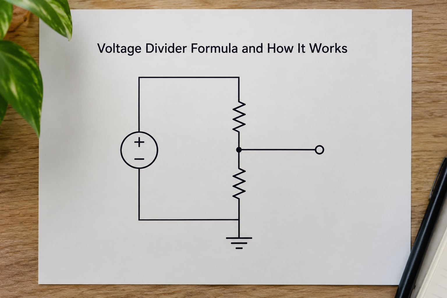
The output voltage of a two-resistor divider is Vout = Vin x R2/(R1+R2), where Vin is the input voltage, R1 is the resistor from the input to the output node, R2 is the resistor from the output node to ground, and Vout is the voltage measured from the output node to ground.
It comes from Ohm’s Law and Kirchhoff’s Voltage Law. The series pair has a total resistance of R1+R2, so the current flowing is I = Vin/(R1+R2). The same current flows through R2, and by Ohm’s Law the drop across R2 is I x R2. Substituting gives Vout = Vin x R2/(R1+R2).
The same derivation works for any impedance, not just resistors, as long as the two elements are in series and nothing else draws current from the output node:
Vout = Vin x Z2/(Z1+Z2)
That is why capacitors and inductors can be used as a divider too, and why a capacitive divider loses accuracy as frequency rises.
Ratios worth memorising
For mental arithmetic on the bench, three ratios cover most of what you meet:
- Equal resistors, R1 = R2, give exactly half the input voltage.
- R1 twice R2 gives one third of the input voltage.
- R2 ten times R1 gives ten elevenths, about 91 percent, of the input voltage.
Inverting those values gets you the other direction. R1 = 2R2 gives two thirds of the supply, and R1 = 10R2 gives ten elevenths of it.
Rearranging the formula
Design work runs the equation backwards more often than forwards. If you know the input and the target output, the resistance ratio falls straight out:
R1 = R2 x ((Vin / Vout) – 1)
For a 12 V input and a 3.3 V target, R1 = R2 x (3.636 – 1) = 2.636 x R2. Pick a friendly R2, multiply, and you have R1.
Voltage Divider Design Step by Step
Here is the procedure I use before soldering anything. It takes a few minutes and catches the mistakes that otherwise show up as a wrong reading on the bench.
The seven-step design procedure
- Write down the requirements. Minimum and maximum Vin, the target Vout at nominal Vin, the highest Vout you can tolerate, the input impedance of whatever reads the output, and the accuracy you need. Missing the last two is where most designs go wrong.
- Compute the ideal ratio. Divide Vout by Vin to get k, then set R1 = R2 x ((1/k) – 1).
- Pick the nearest standard values. Choose R2 first, then the closest available R1, and work out the actual ratio the real parts give you.
- Set the divider current. Total series resistance decides everything downstream, so choose it deliberately rather than picking whatever is in the parts bin.
- Check loading. Compare the divider output impedance, R1 parallel R2, against the load. If they are within a factor of ten, buffer the output.
- Check power. Compute P = V x I or P = V squared / R for each resistor separately and confirm it sits below the rating you intend to use.
- Check tolerance. Add the two tolerances to get worst-case ratio error, and check the source voltage itself is accurate enough for the job.
Verify it on the bench
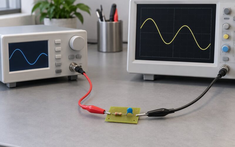
Measure the output before anything is connected, then connect the load and measure again. If the two readings differ by more than a few percent, the divider is being loaded and you need lower impedance values or a buffer.
Check the result against your calculation at the extremes of the input range, not just at one voltage. A divider that reads correctly at 12.0 V can be well over the limit at 14.4 V, and that gap is where field failures live.
How to Choose Resistor Values
You cannot buy 26.36 kΩ. You buy what the table has, then live with the error. That is where most beginner guides stop and this one keeps going.
Standard values and how the rounding error works
Resistors are sold in preferred series. E24 gives 24 values per decade, about 5 percent apart. E96 gives 96 per decade, about 1 percent apart. E192 tightens it further, and precision dividers use 0.1 percent and 0.01 percent parts outside the preferred tables entirely.
Work the example through. Suppose you want a 12 V input scaled to 3.3 V. The ideal ratio is 3.3/12 = 0.275, so R1 = 2.636 x R2. Take R2 = 10 kΩ, giving R1 = 26.36 kΩ.
From the E96 series the nearest value is 26.7 kΩ. The real output becomes:
Vout = 12 x 10/(26.7 + 10) = 12 x 0.2725 = 3.27 V
That is 3.27 V against a 3.30 V target, an error of about minus 1 percent. For an ADC input that is a gift, because the reading never exceeds the target. If you need the output centred instead, pick 26.1 kΩ and land at 3.32 V, about plus 0.7 percent.
The lesson is not that 5 percent parts are fine. It is that you choose the direction of the error deliberately, toward the safe side, because the tolerance stack will add to it either way.
Why smaller values are usually better
Two error sources shrink as you lower the divider impedance: thermal noise, and susceptibility to leakage from the node you are measuring. Standard thick-film parts run roughly 100 ppm per degree Celsius of temperature coefficient, and that drift scales with resistance too.
The cost of going lower is current. Halving the series resistance doubles the standing current and doubles the dissipation. Most designs settle in the 10 kΩ to 100 kΩ range for measurement and sensing, which keeps milliamp-scale current and millivolt-scale noise in comfortable territory.
Which tolerance do you actually need
Absolute tolerance is the spread between the marked value and the real value. What matters for a divider is ratio tolerance, which is smaller than the sum of the absolute tolerances because the two errors partly cancel.
| Absolute tolerance of each part | Worst-case ratio error | Typical use |
|---|---|---|
| 5 percent | about 10 percent | Rough sensing, battery indication |
| 1 percent | about 2 percent | General analog front ends |
| 0.1 percent | about 0.2 percent | ADC range scaling, precision bias |
| 0.01 percent matched pair | 0.01 to 0.05 percent | Instrument references, precision dividers |
Two 1 percent resistors can be off by 2 percent in ratio in the worst case. That is why using 1 percent parts for a supposed reference voltage frustrates people, and why matched pairs or resistor networks exist for the precision path.
Loading Effects and Output Impedance
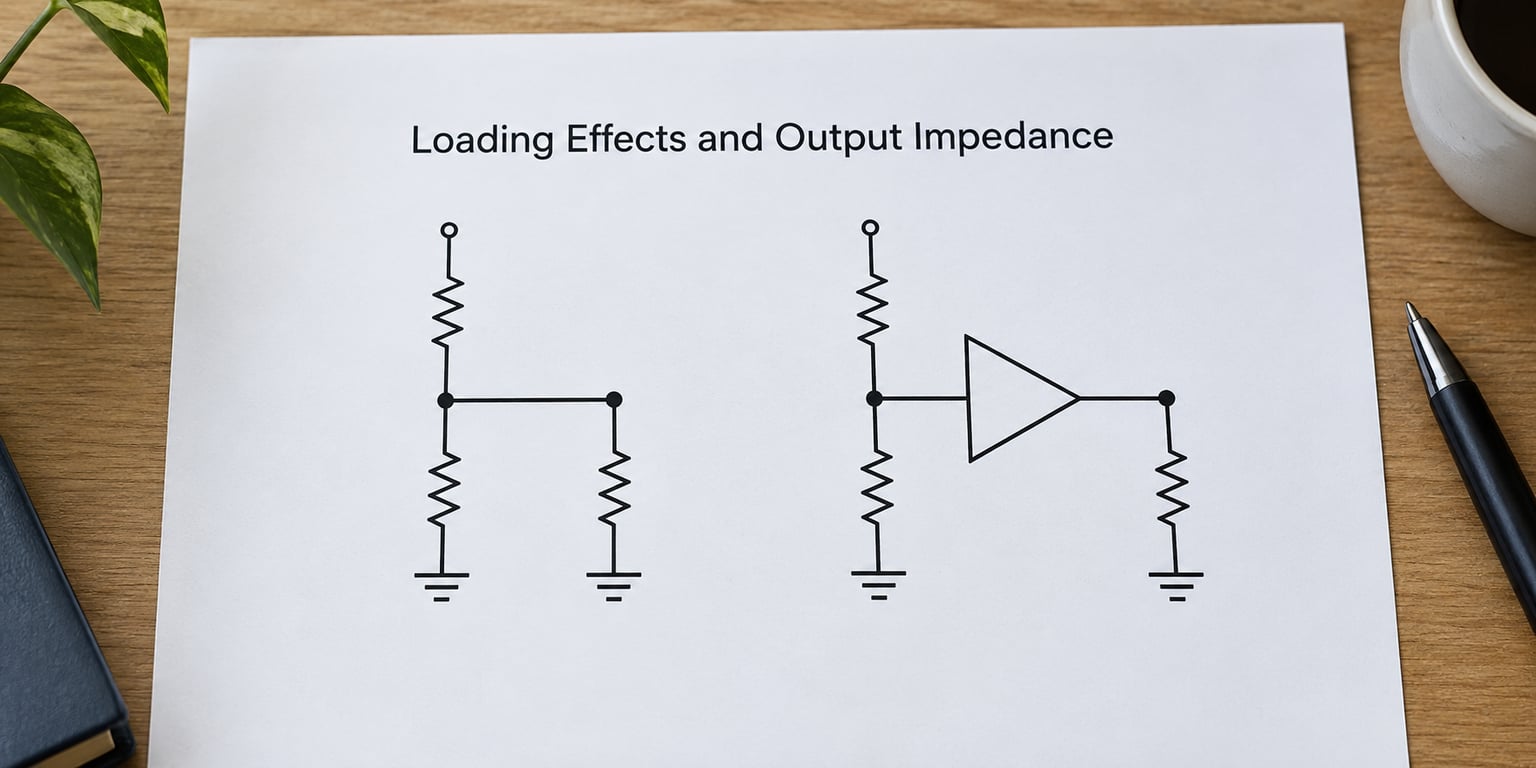
A divider is accurate only when nothing draws current from its output. The moment you connect a load, the output voltage drops, and the size of that drop is set by one number: the Thevenin equivalent resistance of the divider seen from the output node, which is R1 in parallel with R2.
Rth = R1 x R2 / (R1 + R2)
With a load RL connected, the actual output is:
Vout_loaded = Vout_unloaded x RL / (Rth + RL)
Everything reduces to the ratio of RL to Rth.
| Load compared with Rth | Output error | What happens |
|---|---|---|
| 2 x Rth | minus 33 percent | Output collapses |
| 5 x Rth | minus 17 percent | Reading is clearly wrong |
| 10 x Rth | minus 9 percent | Often acceptable |
| 20 x Rth | minus 5 percent | Comfortable |
| 100 x Rth | minus 1 percent | Effectively unloaded |
The 10x loading rule
The rule in one line: keep the load resistance at least ten times the divider’s output impedance, Rload greater than or equal to 10 x (R1 parallel R2), which caps the error at about 9 percent. Makers who learn this one lesson usually stop chasing phantom sensor faults.
Two cases cause most of the confusion. First, an ADC input is not a high-impedance input. The sample-and-hold capacitor draws a brief charging current, and on some parts the datasheet input leakage alone is enough to shift a high-impedance divider. Second, the next stage after the divider determines everything, and it is often a microcontroller pin nobody checked.
For the 12 V to 3.3 V example with 26.7 kΩ over 10 kΩ, the output impedance is 7.3 kΩ. A 100 kΩ load would still pull the reading down by roughly 7 percent. Dropping to 2.67 kΩ and 1 kΩ brings the output impedance to about 730 Ω, and the same load is now fine, at the cost of roughly ten times the standing current.
Buffering the output
An op-amp in the voltage-follower configuration solves loading cleanly. Wire the output to the inverting input, feed the non-inverting input from the divider, and the buffer presents a very high impedance to the divider while driving the load from its own output stage.
Two caveats. The input common-mode range of the op-amp has to include your output voltage, which rules out a lot of single-supply parts at 5 V and above. And the buffer draws its own supply current, so on a low-power design the extra current may matter more than the loading did.
Power Rating and Resistor Safety
Each resistor in the divider dissipates real heat. The larger one, the one taking most of the voltage, dissipates most of the power, and forgetting that is how a divider dies on a 24 V or 48 V bus.
Two equivalent formulas are useful. For each resistor, P = V x I with V being the voltage across that resistor and I the series current. Or, directly from the supply, P = V squared / R for a single resistor sitting across a supply.
Take the 12 V example with 26.7 kΩ and 10 kΩ. The series current is 12/36.7 kΩ = 0.327 mA. Power in the top resistor is 0.327 mA x 8.73 V = 2.9 mW. Power in the bottom is 0.327 mA x 3.27 V = 1.1 mW. Both sit well inside a 0402 part rated at 1/16 W, with plenty of margin for temperature rise.
Two rules make this safe in practice:
- Derate. Design for half the rating or less. A 1/4 W part running at 1/8 W has headroom for an ambient temperature well above room and for tolerance stack-up in the supply.
- Watch self-heating, not just rating. A resistor that sits near half its rating rises in temperature, resistance rises with temperature, and the ratio drifts. That is a temperature coefficient problem wearing a power problem’s clothes.
For high-voltage dividers there is a second limit: the working voltage of the part itself, which is separate from the wattage rating and frequently lower than people expect. Spreading a single high-voltage drop across several resistors in series fixes it. A 48 V bus at 1.47 MΩ puts about 44.7 V across the single top resistor, which is beyond the working voltage of most small film parts. Splitting that into four 330 kΩ resistors in series brings each one to about 11 V and spreads the heat as well.
For mains-adjacent work, use safety-rated high-voltage resistor networks rather than ordinary parts. The approval rating is the whole point of them.
Common Voltage Divider Design Examples
Scaling a 12 V battery to a 3.3 V ADC input
You have a supply running 9 V to 14.4 V and a 3.3 V ADC with a full-scale input of 3.3 V that must never be exceeded.
Target ratio k = 3.3/14.4 = 0.229, so R1 = 3.36 x R2. Taking R2 = 10 kΩ gives R1 = 33.6 kΩ, and the nearest E96 value is 34.8 kΩ.
At the maximum input, Vout = 14.4 x 10/44.8 = 3.21 V. At the minimum input of 9 V, Vout = 9 x 0.223 = 2.01 V. Output impedance is 34.8 kΩ parallel 10 kΩ = 7.8 kΩ.
Series current is 14.4/44.8 kΩ = 0.32 mA, and the top resistor dissipates 0.32 mA x 11.2 V = 3.6 mW. The design is complete, and every number checked.
Shifting a 5 V logic signal down to 3.3 V
The ratio here is 3.3/5 = 0.66, so R1 = 0.515 x R2. With R2 = 10 kΩ, the nearest E96 value for R1 is 5.1 kΩ, giving Vout = 5 x 10/15.1 = 3.31 V.
Check the two things that usually spoil this circuit. First, the receiving input must have a high impedance, because a 3.3 V microcontroller pin in its alternate-function mode is often not one. Second, look at the rising edge: 10 kΩ driving roughly 50 pF of input capacitance gives a rise time of about 0.35 microseconds. Fine for a slow status line, wrong for anything near a megahertz.
Two dividers, one on each side, give better noise immunity than a single divider in the middle when the signal crosses a cable.
Reading a thermistor with a microcontroller
An NTC thermistor with 10 kΩ at 25 degrees sits above a 10 kΩ pull-up resistor to 3.3 V, with the ADC reading the junction. At 25 degrees the divider sits at half scale, 1.65 V, and the voltage falls as temperature rises.
A B-value thermistor changes roughly 4.4 percent per degree near room temperature, so the useful range of a 3.3 V reference with a 1.65 V midpoint gives you about 1.65 V divided by 0.044 V per degree, or roughly plus or minus 37 degrees. That is a good match for room-temperature monitoring.
Where your available resistance range is wide, pick the fixed resistor as the geometric mean of the sensor’s resistance at each end: R_fixed = the square root of R_min times R_max. For a sensor spanning 2 kΩ to 50 kΩ, that gives 10 kΩ, and it maximises the output swing across the range.
Biasing an NPN transistor
On a 5 V supply, target roughly 0.8 V at the base so a 0.7 V junction leaves 100 mV across a 180 Ω emitter resistor for about 0.55 mA of collector current.
R1 = 47 kΩ and R2 = 10 kΩ gives a base voltage of 5 x 10/57 = 0.877 V, which is close. The Thevenin resistance at the base is 47 kΩ parallel 10 kΩ = 8.24 kΩ, and the base impedance of the transistor adds to that in the stability calculation. Compare 8.24 kΩ against a bias network of a few kilohms and the divider is doing real work. Compare it against a megohm and the divider does nothing useful and you should use a fixed base resistor with emitter feedback instead.
Measuring a 48 V bus safely
Divide 48 V down to something a 3.3 V ADC can read. The ratio is 3.3/48 = 0.0688, giving R1 = 13.55 x R2. With R2 = 100 kΩ, R1 comes to 1.36 MΩ and the nearest E96 value is 1.37 MΩ, which puts the output at 48 x 100/1470 = 3.27 V.
Series current is 32.7 microamps, so the power in the whole chain is about 1.6 mW. The problem is not power, it is that nearly 45 V sits across one small resistor. Split the top leg into four series resistors and the design is done.
Protect the ADC against transients too. A 24 V load dump can put a spike far past the 3.3 V pin limit even with the divider fitted. A series resistor close to the pin plus a low-capacitance clamp to ground is the usual answer.
How to Improve Divider Accuracy
Once the topology is right, accuracy comes down to four separate errors, and it pays to know which one is actually hurting you.
Ratio tolerance instead of absolute tolerance
This is the point that beginner guides skip. The worst-case ratio error of a two-resistor divider is (t1 + t2) x R1/(R1+R2), where t1 and t2 are the two absolute tolerances. When R1 is much larger than R2, the expression approaches t1 + t2, so the ratio error approaches the sum of the two absolute tolerances and the parts’ matching matters more than their individual accuracy.
A thin-film resistor pair in a single package has a ratio tolerance of 0.01 or 0.05 percent, far tighter than two independent parts, because both resistors are trimmed on one substrate and track temperature together. That is the cheap route to precision. SOT-23 resistor networks and dedicated high-voltage dividers extend the idea. Decade dividers give 0.001 percent accuracy at the cost of size and cost, and programmable dividers give digital control when you need to change the ratio in firmware.
Buffering and the ADC front end
A voltage follower removes loading almost completely. It does not remove the divider’s own tolerance, and it does add its own offset and noise, so it is not automatically the answer.
On the ADC side, the sample-and-hold capacitor needs time to charge through the divider impedance. Most datasheets specify an acquisition window in samples, and a 10 kΩ divider against a fast-moving input can still read low. Either lower the impedance, buffer it, or slow the sampling.
Some ADCs oversample their reference pin. A divider feeding the reference input is a common source of gain error, which is why running the reference at a fraction of the supply is usually discouraged unless the ADC is specified for it.
Noise, leakage and layout
Johnson-Nyquist noise on the output node comes from the parallel combination of the two resistors, V = the square root of 4kTR, with R taken as R1 parallel R2 and T in kelvin. That is the floor you cannot design below, and it is the reason a 1 MΩ divider is often quiet enough for a 12-bit conversion only in a very quiet layout.
Leakage matters in the same circuits. Board contamination, a flux residue, or even humidity can leak tens of nanoamps across a high-impedance node, and at 1 MΩ that is tens of millivolts of error. Guard rings, a clean board, and conformal coating are cheaper than a lower-impedance design when the impedance is high.
Layout is mostly about keeping the output node short and away from switching nodes. A millimetre of trace next to a fast edge picks up more noise than the divider’s own thermal floor.
When a divider is the wrong tool
Reach for something else when any of these are true:
- You need to power a load. A divider cannot source current usefully. Use a linear regulator or a switching regulator.
- You need a stable reference. Divider accuracy inherits every tolerance in the supply and both resistors. Use a voltage reference IC.
- The load varies. Output voltage now depends on the load. Buffer the divider or regulate properly.
- Efficiency matters. Everything the divider does not pass into the load becomes heat in the resistors.
- The ratio must be precise. Beyond about 1 percent, use a matched network or an active divider.
| Approach | Use it for | Watch out for |
|---|---|---|
| Resistive divider | Sensing, biasing, ADC range scaling, level shifting | Loading, tolerance stack, power dissipation |
| Linear regulator | Powering a load from a higher rail | Heat, dropout, quiescent current |
| Switching regulator | Power where efficiency matters | Noise on the output, layout complexity |
| Voltage reference IC | Accurate references for ADCs and DACs | Cost, minimum load current |
| Op-amp buffer | Driving a load from a divider | Common-mode range, offset, supply current |
Troubleshooting the symptoms people actually hit
Almost every divider problem shows up as one of a handful of symptoms. Matching the symptom to the cause is faster than re-deriving the formula for the fourth time.
| Symptom | Likely cause | Fix |
|---|---|---|
| Output reads lower than calculated | Load or ADC input drawing current | Lower the divider impedance or buffer the output |
| Output reads lower than calculated, only at high input voltage | Resistor self-heating raising resistance | Lower dissipation or move to a higher rating part |
| Reading drifts with temperature | Temperature coefficient plus supply drift | Use thin-film parts and a low-TCR source, or correct in firmware |
| Reading is noisy or jumping | Thermal noise, high impedance, nearby switching nodes | Add an RC filter, lower impedance, reroute the trace |
| ADC reads low on fast-changing input | Sample-and-hold capacitor not settled | Increase acquisition time or buffer the divider |
| Output is far too high | R1 and R2 fitted in the wrong positions | Check the schematic against the board orientation |
| Output only correct at one supply voltage | Design checked at nominal only | Recalculate at Vin max and Vin min |
| Resistor too hot to touch | Undersized package for the dissipation | Raise the resistance, split it across series parts, derate the design |
The first row is the one people search for most. If the divider is correct with a meter attached and wrong with the sensor attached, it is loading, and no amount of recalculating the ratio will fix it.
A short checklist before you solder
- R1 and R2 are not swapped. A swapped pair usually means Vout sits near the supply instead of near ground, and on an ADC pin that is a damaging fault.
- The divider output is checked against the maximum input voltage, not the nominal.
- The load impedance was found and compared with R1 parallel R2.
- The input impedance of the ADC or logic pin was looked up.
- Power was checked on both resistors, separately.
- Working voltage was checked on any resistor taking more than about 40 V.
- Rounding to standard values was done deliberately, in the safe direction.
Frequently Asked Questions
What is the minimum resistance I should use in a voltage divider?
There is no single minimum, but the usual range is 10 kOhm to 100 kOhm for measurement and sensing. Below that, standing current and heat rise without adding much accuracy. Above it, thermal noise and board leakage start to eat into your resolution. Pick the highest value that still meets your noise and loading requirements, then check power dissipation.
Can a capacitor be connected to the output of a voltage divider?
Yes, and it is often a good idea. A small capacitor from the output to ground filters noise and helps the sample-and-hold capacitor on an ADC settle faster. Keep it small, since it also forms a low-pass filter with the divider output impedance, and check the resulting cutoff frequency against the signal bandwidth you need.
How do I calculate the power rating of divider resistors?
Compute the series current first: I equals Vin divided by the total series resistance. Then multiply that current by the voltage across each resistor separately, or use P equals V squared over R for the resistor in question. Design for half the package rating or less to leave margin for ambient temperature and supply tolerance.
Why does my divider output change when I connect a load?
Because a divider has output impedance equal to R1 in parallel with R2, and connecting a load forms a divider with that impedance. The output becomes Vout times RL divided by Rth plus RL. Either lower the divider impedance, raise the load impedance, or buffer the output with an op-amp voltage follower.
When should I use an op-amp buffer after a voltage divider?
Buffer whenever the load impedance is less than about ten times the divider output impedance, whenever the next stage has a biased or low input impedance, or when the input is a fast-moving signal feeding an ADC. Check that the op-amp supply range covers the output voltage, since many single-supply parts cannot swing near their positive rail.
What is the 10% rule for voltage dividers?
It is a loading guideline: keep the load resistance at least ten times the divider output impedance, which is R1 in parallel with R2. At that ratio the error is capped at roughly 9 percent. For tighter accuracy, go to twenty or a hundred times. VDR is the voltage divider rule, the same formula applied to voltages; CDR is the current divider rule, its counterpart for two parallel branches.
Conclusion
Voltage divider design explained comes down to four checks in order: get the ratio right, round to real standard values and measure the resulting error, keep the load at least ten times the divider output impedance, and confirm each resistor stays well under its power rating and working voltage.
Start with the ratio calculation, then work outward. Pick R2, solve R1, find the nearest value that exists, and write down the actual output rather than the ideal one. Everything after that is a check on whether that output survives contact with the real circuit.