A buck converter is a DC-to-DC step-down power converter that reduces a higher input voltage to a lower, regulated output voltage by repeatedly switching the input through an inductor and filtering the result with a capacitor. It does this at high efficiency, typically 85 to 95 percent, because it moves energy rather than burning off the difference as heat. The whole operation comes down to one relationship: the output voltage equals the input voltage multiplied by the duty cycle, so Vout = D x Vin.
That is the short version. The useful version is what happens electrically during each part of the switching cycle, which is what the rest of this guide builds up.
Table of Contents
- How Does a Buck Converter Step Down Voltage?
- The Main Parts of a Buck Converter
- Buck Converter Operation Explained: The Switching Cycle
- Continuous, Discontinuous, and Critical Conduction Modes
- How the Feedback Loop Regulates the Output
- Key Design Equations and Design Limits
- Buck Converter Efficiency, Losses, and Thermal Behavior
- Buck Converter Operation Explained with a Simple Example
- Frequently Asked Questions
- How does a buck converter circuit work?
- Can you explain how a DC-DC buck converter works?
- What are the downsides of using a buck converter?
- How does a buck-boost converter work?
- Do I need a buck converter or an LDO?
- Why is the inductor current continuous in a buck converter?
- Conclusion
How Does a Buck Converter Step Down Voltage?
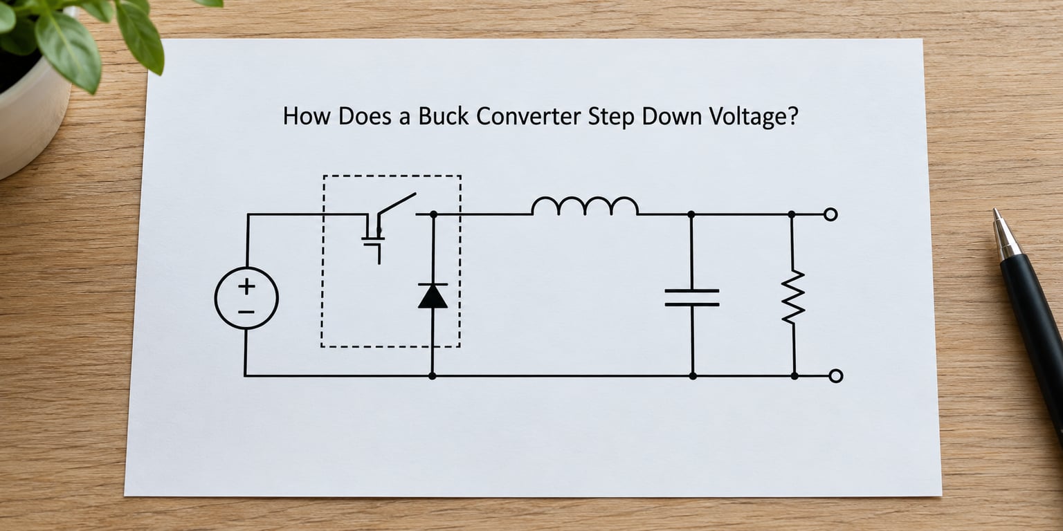
It is called a step-down converter for the same reason a gear reducer is called a reducer: the output voltage is always lower than the input. A buck cannot produce 12 V from a 5 V supply, no matter how the controller is configured.
Stepping down works because a switch node is a pulse train, and an inductor plus capacitor acts as a low-pass filter that averages that pulse train. The controller sets the pulse width, and the filter converts the average into a steady DC level. Change the pulse width and you change the average, which is why duty cycle is the output control knob.
Four quantities get confused constantly, so it is worth separating them:
- Input voltage (Vin) is what the supply rail delivers before conversion.
- Output voltage (Vout) is the regulated rail the load sees.
- Current flows through the inductor in pulses that are smoothed into a near-DC value at the output.
- Power is voltage multiplied by current, and in a healthy converter almost all of the input power reaches the load. What does not make it appears as heat.
That last point is the whole reason to use a switching converter. If you drop 12 V to 3.3 V with a linear regulator at 1 A, the regulator dissipates (12 – 3.3) x 1 = 8.7 W. A buck converter moving the same current turns 11.1 W in and about 10.2 W out, so the loss is closer to 0.9 W spread across the inductor and the switches.
The Main Parts of a Buck Converter
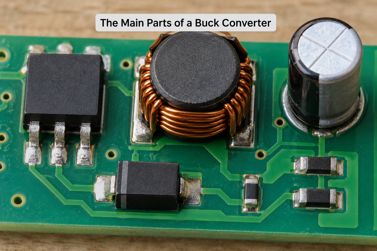
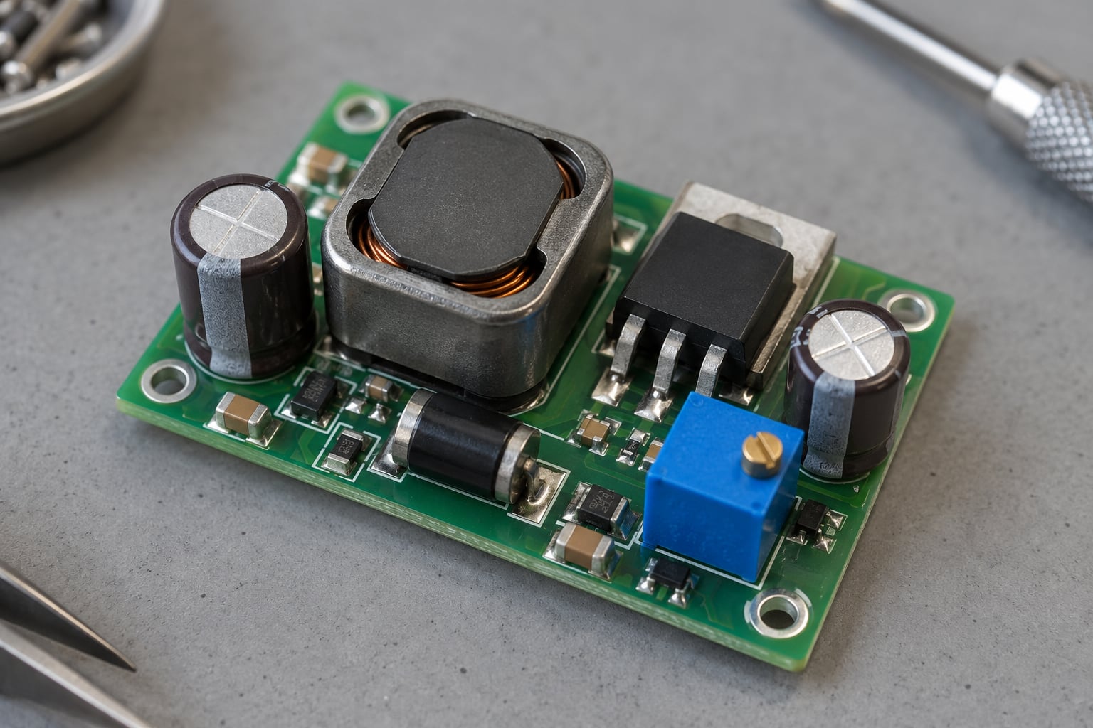
Every buck converter, from a four-dollar module to a controller driving dozens of amps, is the same set of parts doing the same four jobs. Knowing which part does what turns a schematic into something you can reason about.
| Component | Job | During switch ON | During switch OFF |
|---|---|---|---|
| High-side switch (MOSFET) | Connects Vin to the switch node | Conducts, acting as a closed switch | Blocks, isolating the input |
| Low-side switch or freewheeling diode | Provides a current path when the input is disconnected | Blocks (diode reverse biased) or held off | Conducts, carrying inductor current to ground |
| Inductor | Stores energy in a magnetic field and smooths current | Current ramps up, field energy builds | Field collapses and drives current onward |
| Output capacitor | Absorbs the current difference and holds Vout steady | Charges, since the load draws less than the inductor supplies | Discharges into the load, covering the current dip |
| Feedback divider | Samples Vout and reports it to the controller | Sampling continues unchanged | Sampling continues unchanged |
| Controller | Compares feedback to a reference and drives the duty cycle | Drives the high-side gate on | Drives the high-side gate off, after a short dead time |
Two topologies use the second row differently. A nonsynchronous buck uses a Schottky freewheeling diode, which turns on automatically whenever the switch node goes negative. A synchronous buck replaces that diode with a second MOSFET driven by the controller, which costs extra control logic but cuts conduction loss at low output voltages.
Either way the current loop during the off interval runs from ground, through the lower switch, up through the inductor, and out to the load. There is no path to the input during that time, which is the whole point.
Buck Converter Operation Explained: The Switching Cycle
The controller works at a fixed switching frequency and modulates the on-time within each period. Everything else follows from the two states that on-time creates.
Switch ON (charging phase). The high-side MOSFET closes and connects the input voltage to the inductor. Because an inductor resists sudden changes in current, the current through it ramps up rather than jumping, and along the way the inductor stores energy in its magnetic field. The output capacitor sees more current arriving than the load is taking, so it charges and its voltage rises slightly above the target.
Switch OFF (discharging phase). The high-side MOSFET opens and there is no longer a path to the input. The inductor reverses its voltage polarity to keep the current flowing in the same direction, and the freewheeling diode or low-side MOSFET provides that path. The output capacitor now supplies more current than the inductor delivers, so it discharges and its voltage dips slightly below the target.
Repeat those two states tens of thousands of times a second and the dips and rises blur into a small ripple riding on a steady DC level. Volt-second balance is the formal statement of why that level sits where it does: in steady state the average voltage across the inductor must be zero, otherwise the current would keep ramping up without bound. That gives D x Vin – (1 – D) x Vout = 0, which rearranges to Vout = D x Vin.
So if Vin is 12 V and you want 5 V, the controller settles near a duty cycle of 5/12, or about 42 percent. Drop the load and the feedback loop will not change the duty cycle to compensate, because the average inductor voltage stays zero either way. Regulation happens in the other direction entirely, by adjusting the duty cycle to hold the output where the loop commands.
Continuous, Discontinuous, and Critical Conduction Modes
How the inductor current behaves depends on whether the load is heavy enough to keep the current from ever reaching zero.
Continuous conduction mode (CCM) means the inductor current never falls to zero. This is the normal mode at medium and heavy loads, and it is the mode most datasheets assume when they quote efficiency. The switching waveform is steady, the feedback loop has a predictable plant to control, and the ripple current is a fixed peak-to-peak triangle.
Discontinuous conduction mode (DCM) means the inductor current falls to zero partway through the off interval and stays there for a while. It happens at light loads, when the load cannot absorb the current the inductor is delivering. The third interval, with zero current everywhere in the power stage, is why light-load efficiency depends so much on how the controller handles those dead periods.
Critical conduction mode (CCM/DCM boundary) is the exact load current where the minimum of the ripple triangle just touches zero. Designers often target this boundary deliberately, because above it the converter enters CCM where ripple stops being a function of load and the design becomes predictable.
Most controllers deal with light load by switching between pulse-width modulation and pulse-frequency modulation, or by going into a burst pattern that skips whole switching cycles. That is why quiescent current specifications matter for battery-powered designs: a converter can be perfectly efficient at 500 mA and still ruin a cell life at 50 microamps of standby draw.
How the Feedback Loop Regulates the Output
Volt-second balance tells you the relationship between duty cycle and output. The feedback loop is what holds the duty cycle at the right value, and it works by measuring the output and correcting the error.
Two resistors divide the output voltage down to a small feedback signal at the FB pin of the controller. An internal voltage reference, commonly around 0.6 V to 0.8 V, is compared against that signal by an error amplifier. When the output sags below target, the feedback signal falls below the reference, the error amplifier drives its output up, and the controller lengthens the on-time. More on-time raises the average switch node voltage, which pushes more current into the output and pulls the voltage back up. The loop then repeats in the other direction when the output rises too far.
Because output voltage sets the feedback level, the divider itself is the output voltage setting. Changing the upper resistor changes the rail the converter regulates to, which is why a single design can be a 3.3 V part or a 5 V part with two resistor values.
Voltage-mode control compares only the output voltage. Current-mode control also measures the current through the low-side switch, typically with a small sense resistor, and uses it in a second inner loop. That inner loop makes the control respond to load changes before the output voltage has moved, which gives better transient response and allows the duty cycle to be limited directly by the peak current setting.
The other block worth knowing is the compensation network around the error amplifier. It sets the crossover frequency and phase margin, and it is the piece most often left as a copy-paste from the reference design because getting it wrong produces instability that shows up as oscillation or a slow ringing transient rather than an obvious failure.
Key Design Equations and Design Limits
Most of the sizing work in a buck converter is four equations and a set of limits that will not bend.
Duty cycle. D = Vout / Vin, ignoring losses. In practice you need headroom for the voltage drop across the high-side and low-side switches, so designs usually keep the ideal duty cycle away from 100 percent. A common rule of thumb is to allow at least 10 percent margin, which caps a 5 V output on a 5.5 V input rather than letting it sit at 91 percent duty.
Inductor ripple current. The peak-to-peak ripple in CCM is Delta I = (Vin – Vout) x D / (L x fsw), and since D x Vin is approximately Vout, this is often written as Delta I = Vout x (1 – D) / (L x fsw). Inductor manufacturers allow roughly plus or minus 20 percent tolerance, so size the inductor so that the peak current, which is Iout plus half the ripple, stays below the saturation current even at the low end of that tolerance.
Most designs target ripple between 10 and 60 percent of the load current. Below 10 percent you get a smooth output, but it costs you a large inductor and a slow transient response. Above 60 percent the peak current approaches twice the load current, which pushes up RMS losses in the inductor and the switches and erodes the efficiency you were buying.
Output ripple voltage. Ripple comes from two independent sources: the charge and discharge of the capacitor, and the voltage developed across the capacitor’s equivalent series resistance. The ESR term is Delta I x ESR, and it is the one that surprises people. Adding capacitance barely touches it, because the ESR does not shrink. Ceramic capacitors have low ESR and give much less ripple than electrolytics, but their effective capacitance falls with DC bias and temperature, which is a separate trap.
Switching frequency. A higher frequency means a smaller inductor and smaller capacitor for the same ripple, but more switching loss and more EMI. A lower frequency is more efficient and quieter, but needs bigger magnetic components and slows the loop down. Most general-purpose controllers sit between roughly 300 kHz and 2 MHz.
Ratings and limits. The input must stay inside the controller’s operating range, the output current must stay under both the switch current limit and the inductor’s rating, and the feedback divider’s power dissipation matters at high output voltages since the divider burns current continuously. The low-side switch or diode must block the full output voltage every cycle, and the inductor’s insulation and DCR both matter for the design’s loss and thermal budget.
Buck Converter Efficiency, Losses, and Thermal Behavior
Efficiency in a buck converter is the input power minus the output power, divided by input power, and every watt that is missing ends up as heat in the inductor, the switches, or the controller.
| Loss mechanism | Where it happens | What drives it |
|---|---|---|
| Conduction loss | High-side and low-side switches during the on and off intervals | On-resistance multiplied by RMS current, highest at low output voltage |
| Switching loss | At the transition as the switch changes state | Vin, Iout, frequency, and the voltage and current overlap during the transition |
| Gate drive loss | Charging and discharging the MOSFET gate capacitance | Total gate charge multiplied by gate drive voltage and frequency |
| Dead-time loss | The gap between the two switches turning off and on | Body diode or opposite conduction during the blanking interval |
| Inductor loss | Copper and core losses in the magnetic component | RMS ripple current, winding resistance, core material |
| Capacitor loss | ESR dissipation in the output capacitor | Ripple current multiplied by ESR |
Two patterns follow from that table. Efficiency peaks somewhere in the middle of the load range, because at heavy load conduction and switching loss dominate, and at light load fixed losses like gate drive dominate. Peak efficiency is normally quoted near 50 to 80 percent of the maximum load current, so a converter specified at 92 percent at 3 A may be nearer 70 percent at 100 mA.
Thermal behavior follows the same curve. A converter dissipating 0.9 W in a small package at room temperature has plenty of margin, but the same part dissipating 9 W during a load step needs a copper area or a heat sink. The junction temperature is the ambient temperature plus the power loss times the thermal resistance from junction to ambient, and thermal shutdown is what stops you before the package limit.
One measurement detail saves a lot of confusion. Switch-node ringing above roughly one third of the input voltage is usually the probe, not the circuit: the probe’s ground lead forms a loop with the oscilloscope input capacitance, and that parasitic inductance resonates with the node capacitance. The standard fix is the ground-spring technique, a short spring or a via stub soldered right at the ground pad, instead of the 15 cm clip lead. Ring that disappears when the lead is shortened, and you have your answer.
Buck Converter Operation Explained with a Simple Example
Take a common bench supply: 12 V in, 5 V out, 3 A maximum, switching at 500 kHz. The design choices follow one after another.
Duty cycle. D = 5/12 = 0.417, or about 42 percent. With losses, expect the controller to sit nearer 45 percent.
Inductor. Targeting ripple at about 30 percent of 3 A gives roughly 0.9 A peak to peak. Delta I = 5 x (1 – 0.417) / (L x 500000) = 0.9, so L is about 6.5 microhenries. A 6.8 microhenry part with a saturation rating above 3.45 A and a DCR in the tens of milliohms range covers it, and it will run in CCM down to roughly 0.45 A of load.
Output capacitor. Allow about 20 mV of ripple. If the chosen ceramics have an ESR of 5 milliohms, the ESR alone contributes 0.9 x 0.005 = 4.5 mV, so the capacitance term has to supply the rest. The off interval lasts (1 – 0.417) / 500 kHz, about 1.17 microseconds, and the current falls by the full 0.9 A across it, a discharge slope near 0.77 A per microsecond. The remaining 15.5 mV divided by that slope gives roughly 20 microfarads, and two 22 microfarad ceramics in parallel with margin for DC bias derating is a reasonable choice.
Losses and efficiency. Take conduction loss in the high-side switch with 20 milliohms on-resistance at about 3.3 A RMS: about 0.22 W. The low-side switch with 15 milliohms at about 2 A RMS: 0.06 W. Switching loss at these numbers lands in the tenths of a watt, gate drive is small at 500 kHz, and inductor and capacitor losses add a few tenths. Total around 0.6 W against an output of 15 W, so roughly 96 percent. The 8.7 W that a linear regulator would have thrown away as heat is now under a watt spread across a few parts.
Worth noting what happens if the load falls to 200 mA: the ripple no longer fits inside the load current, the converter drops into DCM, and the losses that were proportional to current are largely gone. Fixed costs are not, so the curve slopes down on both sides of its peak.
Frequently Asked Questions
How does a buck converter circuit work?
A buck converter repeatedly switches a higher input voltage through an inductor, then filters the result with a capacitor to produce a lower regulated output. While the switch is on, current ramps up through the inductor and the output capacitor charges. While the switch is off, the inductor reverses its voltage to keep current flowing through the load via a freewheeling diode or low-side MOSFET, and the capacitor discharges to cover the difference. The average switch node voltage sets the output, giving Vout = D x Vin.
Can you explain how a DC-DC buck converter works?
Think of it as DC to AC to DC without the mains connotation. The controller chops the DC input into a fast pulse train at a square-wave node, and an inductor and capacitor act as a low-pass filter that averages that train back into steady DC. A feedback divider measures the output, an error amplifier compares it to an internal reference, and the controller adjusts pulse width until the two match. Because energy is moved rather than dissipated, typical efficiency is 85 to 95 percent.
What are the downsides of using a buck converter?
The main trade-offs are output ripple, conducted and radiated EMI from the switch node, and a more complex circuit than a linear regulator. Ripple comes from capacitor charge and discharge plus voltage across capacitor ESR. The switch node is a fast edge on a high-voltage node, so layout matters more than with an LDO. Load transient response also depends on loop compensation, and a buck cannot regulate its output up to the input. A linear regulator is still simpler and quieter for a small voltage drop.
How does a buck-boost converter work?
A buck-boost converter inverts the polarity of the inductor during part of the cycle, so the output can be higher than, lower than, or equal to the input. That added freedom costs more: the topology needs two switches and more careful control, and the inverted output complicates downstream design. A four-switch buck-boost keeps the output polarity the same and is common in USB and battery applications. A plain buck is preferred when the output only ever needs to be below the input.
Do I need a buck converter or an LDO?
Compare the drop against the output voltage, not just the current. A linear regulator dissipates (Vin – Vout) x Iout as heat, so a 12 V to 3.3 V conversion at 1 A wastes 8.7 W and needs a large heat sink. A buck moves the same power at roughly 90 to 95 percent efficiency. LDOs still win for small drops of a few hundred millivolts, for very low noise rails, and for fast load transients that matter more than dissipation. Many designs use both in sequence.
Why is the inductor current continuous in a buck converter?
The inductor current stays continuous because of the energy stored in its magnetic field. When the switch opens and cuts off the path to the input, the collapsing field drives the same current onward through the freewheeling diode or low-side switch, and the current simply reverses the sign of the inductor’s voltage to do it. The current ramps down rather than stopping instantly. Only at light loads, when the ramp reaches zero before the next cycle, does it stop and the converter enters discontinuous conduction mode.
Conclusion
That is buck converter operation explained in one line: a switch turns a DC input into a controlled pulse train, an inductor smooths the current, a capacitor smooths the voltage, and a feedback loop keeps the average at the value you asked for by adjusting the pulse width.
If you are analysing or designing one, start at the switch node. Sketch the two current paths on paper, mark the voltages across the inductor in each state, and confirm that the on-time and off-time average to zero. Everything else, ripple, mode of operation, loop stability, and where the heat goes, follows from that sketch.