Burn in testing for semiconductors is a screening step where devices are held at elevated temperature, usually with elevated supply voltage and continuous current, for hours to days so that latent defects fail inside the factory instead of in a customer’s board. Burn in testing for semiconductors explained in plain terms is mostly a question of physics: raise the temperature, make current flow, and weak spots give themselves away early.
The rest of this guide walks through what gets stressed, which failure mechanisms surface first, how the conditions get chosen, and where burn in sits among qualification tests like HTOL and HAST. I have kept the numbers in ranges rather than pretending there is one universal recipe, because there is not.
Table of Contents
- What Is Burn In Testing for Semiconductors?
- Why Semiconductor Burn In Testing Matters
- How Does Burn In Testing Work?
- What Stress Conditions Are Used?
- Temperature
- Voltage and current density
- Load mode: static versus dynamic
- Humidity and cycling
- Burn In Testing vs. Other Reliability Tests
- What Kinds of Failures Can Burn In Reveal?
- Electromigration
- Hot carriers
- Dielectric breakdown and TDDB
- Bond and interconnect weakness
- Latent process and ESD damage
- Parameter drift
- How Is Burn In Testing Performed in Semiconductor Manufacturing?
- What Data and Reliability Metrics Are Collected?
- How Do Engineers Decide Whether Burn In Is Necessary?
- Frequently Asked Questions
- What is a burn-in test for semiconductors?
- What is the purpose of burn-in testing?
- What is the difference between burn-in testing and HTOL testing?
- What is burn testing?
- How long does burn-in testing take and at what temperature?
- Does burn-in testing damage chips that would otherwise work?
- Conclusion: Start With the Device Reliability Risk
What Is Burn In Testing for Semiconductors?
A burn-in test is a reliability screening process in which finished semiconductor devices are stressed well above their normal operating conditions — elevated junction temperature, elevated supply voltage, and steady current — for a set period so that devices with manufacturing defects fail on the test floor instead of in the field. Devices that pass are then binned and shipped with early-life risk already removed.
Five things define any burn in condition, and engineers argue about all five:
- Temperature. The chamber air temperature, which is not the same number as the junction temperature inside the die.
- Voltage. Usually a multiple of the rated supply, commonly 1.1 to 1.3 times nominal.
- Duration. Anywhere from a few hours to 1000 hours, depending on the failure mechanism being screened.
- Load and pattern. Static bias holds a fixed state; dynamic burn in drives functional test patterns through the part.
- Sample size and lots. Whether the whole production lot is burned in, or a statistical sample is taken to validate the process.
| Parameter | Typical range | What it controls | Who sets it |
|---|---|---|---|
| Chamber temperature | 85 °C to 150 °C | How fast degradation mechanisms run | Reliability engineer |
| Supply voltage | 1.1x to 1.3x rated | Current density through metal lines | Test engineer with the design team |
| Duration | 24 h to 1000 h | Whether rare mechanisms get time to appear | Reliability engineer, sometimes the customer |
| Load mode | Static bias or dynamic patterns | Whether internal logic and memory cells are exercised | Test development team |
| Sample | Full lot or 5 to 77 units per lot | Statistical confidence versus throughput cost | Quality and manufacturing |
One terminology point before going further, because it trips people up constantly. Semiconductor “burn in” has nothing to do with the burn-in effect in LCD or OLED panels, where a static image can leave a permanent ghost. Different physical phenomenon, same two words. When a display supplier says it burn-in-ages its panels, that is unrelated to everything below.
Why Semiconductor Burn In Testing Matters
The reason burn in exists is the bathtub curve. Reliability engineers plot failure rate against time and get a shape like a bathtub: a steep early wall, a long flat floor, and a rising late wall.
The early wall is infant mortality. Defects introduced during wafer fabrication, assembly, wire bonding or handling produce devices whose failure mechanisms are already in motion the moment they are powered. Left alone, that population thins out within the first few hundred hours of use. The flat floor is the useful life of a good device. The late wall is wear-out, where normal ageing mechanisms take over.
Burn in is aimed squarely at the early wall. Rather than waiting for a customer to discover the population, the manufacturer accelerates the early phase inside the factory and throws away what fails. What survives is a population that has already demonstrated a margin.
Concretely, burn in screens out or exposes:
- Weak solder joints and under-driven wire bonds that fatigue under thermal cycling stress.
- Metal line electromigration driven by current density at elevated temperature.
- Hot carrier injection in transistors that have been over-driven beyond their rated supply.
- Time-dependent dielectric breakdown in thin gate oxides that were already marginal.
- Delamination and moisture-related corrosion at package and substrate interfaces.
- Devices with marginal parameter drift, which show up as a slow shift in leakage or timing rather than a hard stop.
It is most worth doing where field failures are expensive and the population is small enough that an escape is visible. Automotive, medical, aerospace, defence and telecom parts are the classic cases. For high-volume consumer silicon with a mature process and a well-characterised failure history, the same hours can be better spent elsewhere.
How Does Burn In Testing Work?
The mechanism is acceleration. Most semiconductor degradation mechanisms are thermally activated, meaning their rate rises with temperature following an Arrhenius relationship, and the rate roughly doubles for every 8 °C to 10 °C increase in junction temperature over the relevant range.
That is why burn in works at all. A device that would take years to develop a failure at 55 °C can show the same failure in 24 to 100 hours at 125 °C, because the reaction is running thousands of times faster. The practical difficulty is that the acceleration factor is only valid when you know the activation energy for the mechanism you are chasing, and that number is different for electromigration than for bond fatigue.
Because of that, junction temperature matters more than chamber temperature. A chip dissipating several watts in a package on a burn-in board can run 20 °C or more above the air it is sitting in, and the self-heating changes with the pattern being driven. A board that forces devices into a high-toggle state heats its own junction temperature well above a board holding static bias. Measure or model the junction, not just the chamber setpoint.
While the parts soak, the tester watches them. Current draw, supply voltage and, on more sophisticated systems, response to a diagnostic pattern are sampled continuously. A device that drifts by a defined amount, or whose current jumps, is a candidate for rejection. This is the part people forget: burn in is not just a hot oven. It is a monitored stress with a data trail.
What Stress Conditions Are Used?
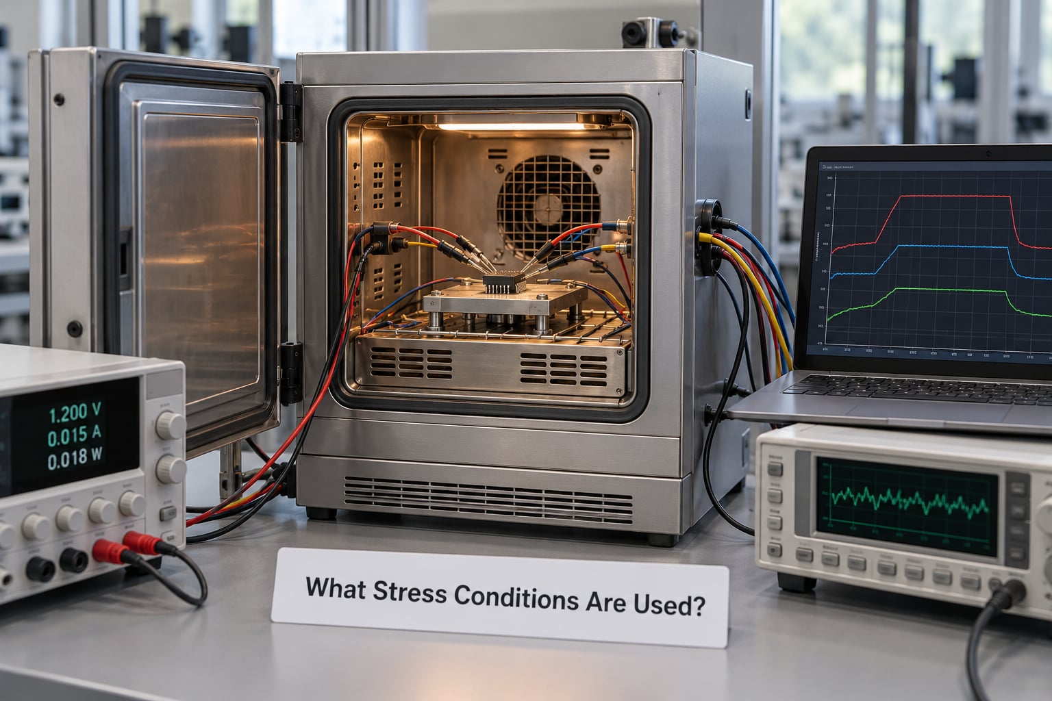
Stress conditions vary by device class, and the useful question is always “which mechanism am I trying to make appear faster”.
Temperature
Chamber setpoints for packaged silicon commonly sit between 85 °C and 150 °C, with automotive and military parts often specified higher than consumer parts. Optoelectronic devices such as laser diodes have their own windows, typically lower, because their output degrades along a different curve.
Voltage and current density
Burn in almost always runs above the rated supply, commonly 1.1 to 1.3 times nominal, to raise current density through metal interconnects. The limit is set by the design: push past what the oxide and junction can hold and you stop screening defects and starting new ones.
Load mode: static versus dynamic
Static burn in holds a fixed bias state with no logic activity. Dynamic burn in drives patterns from a pattern generator or from memory in the tester, toggling the device the way a real system would. Dynamic runs hotter, needs more capable equipment, and exposes far more of the die.
| Aspect | Static burn in | Dynamic burn in |
|---|---|---|
| Bias | Fixed voltage and current, no toggling | Functional patterns drive inputs while power is applied |
| Pattern coverage | Minimal, only the biased nodes are active | Full or partial logic, memory and I/O coverage |
| Junction temperature rise | Lower, steadier | Higher and pattern-dependent |
| Detects | Leakage, static IDDQ drift, gross assembly defects | Those plus state-dependent timing, stuck cells, interconnect opens |
| Equipment | Simpler board and supply, lower cost | Pattern generator or large pattern memory, higher cost |
| Typical use | Cost-sensitive screening of mature parts | High-reliability, high-complexity logic and memory |
Humidity and cycling
Adding humidity or thermal cycling turns burn in into something closer to THB or temperature cycling, which brings a different set of mechanisms such as corrosion and delamination into play. That is a deliberate choice, not a default.
Burn In Testing vs. Other Reliability Tests
Burn in screens production units for early failures; qualification testing proves a design will meet its reliability spec over its intended life.
| Test | Purpose | Typical conditions | Duration | Applied to |
|---|---|---|---|---|
| Burn in | Screen early-life failures from production | 85-150 °C, 1.1-1.3x rated supply, biased | 24 h to 1000 h | Production units or lot samples |
| HTOL | Qualify long-term reliability at elevated temperature | Around 125 °C or the application’s maximum, at rated conditions | 1000 h | Qualification samples of a design |
| HAST | Qualify quickly with combined heat and humidity | 130 °C or above at high relative humidity, biased | Typically far shorter than HTOL | Qualification samples, especially board-level packages |
| THB | Evaluate moisture and bias effects | 85 °C at 85 percent relative humidity, biased | 1000 h | Qualification samples, plastic packages |
| QTH | Qualification test, a controlled-stress programme with defined sample sizes and pass criteria | Defined per the governing programme and standard | Defined per programme | Customer or regulator specified |
The practical difference is intent. HTOL and HAST run a small number of parts for a long time to prove the design. Burn in runs a lot, or a sample of a lot, to make sure the individual unit leaving the line is sound. Confusion between the two is common and leads to over-specifying a screen or, worse, treating a passed qualification as permission to skip screening.
Governing documents matter here. JEDEC JESD22 covers many of the environmental and reliability test methods, MIL-STD-883 Method 1011 covers steady-state temperature and humidity conditions for military parts, and AEC-Q100 defines the automotive qualification stress suite. Where a customer contract names a standard, the standard wins over any internal default.
What Kinds of Failures Can Burn In Reveal?
Electromigration
Current flowing through a metal line moves atoms along it. At elevated temperature the movement accelerates, and a narrowing in the line becomes an open circuit eventually. Burn in catches it while the line is still marginal, because the resistance has already started to climb.
Hot carriers
Carriers injected into an oxide trap there and shift threshold voltage. This is the classic overstress mechanism, and it is why drive stress above the rated supply has to be bounded. Excessive drive converts a screening test into a damaging one.
Dielectric breakdown and TDDB
A thin gate oxide that is close to failing shows leakage growth under field and temperature. Burn in surfaces this as rising IDDQ, which is why leakage monitoring is part of the tester, not an optional extra.
Bond and interconnect weakness
Wire bonds, flip-chip solder joints and package delamination respond to heat cycling and sustained heat. Holding a device hot under bias for hundreds of hours is enough to crack a marginal joint that passed a cold electrical test.
Latent process and ESD damage
Handling damage and latent oxide flaws that do not affect function at room temperature can become hard failures once the device is hot and switching. This is the population burn in is uniquely good at catching, because it only appears under stress.
Parameter drift
The subtlest failure mode. A device that passes every limit but moves steadily in leakage or timing will eventually cross a customer limit. Most testers apply a drift band over the soak so these are binned out rather than discovered later.
How Is Burn In Testing Performed in Semiconductor Manufacturing?
Burn in is one stage in a longer sequence, and its position explains a lot about how it is specified.
- Wafer sort. Devices are probed on the wafer for basic functionality, parametric limits and binning before any money is spent on packaging.
- Dicing and assembly. The wafer is diced, dies are mounted, and wire bond or flip-chip attach happens. This is where a large share of latent defects are physically created.
- Pre-burn electrical test. A room-temperature test confirms the device is functional and records its baseline parameters for later drift comparison.
- Burn-in board loading. Devices are socketed or soldered into a burn-in board, usually hundreds of devices per board, which provides the bias, the power and often the pattern connections.
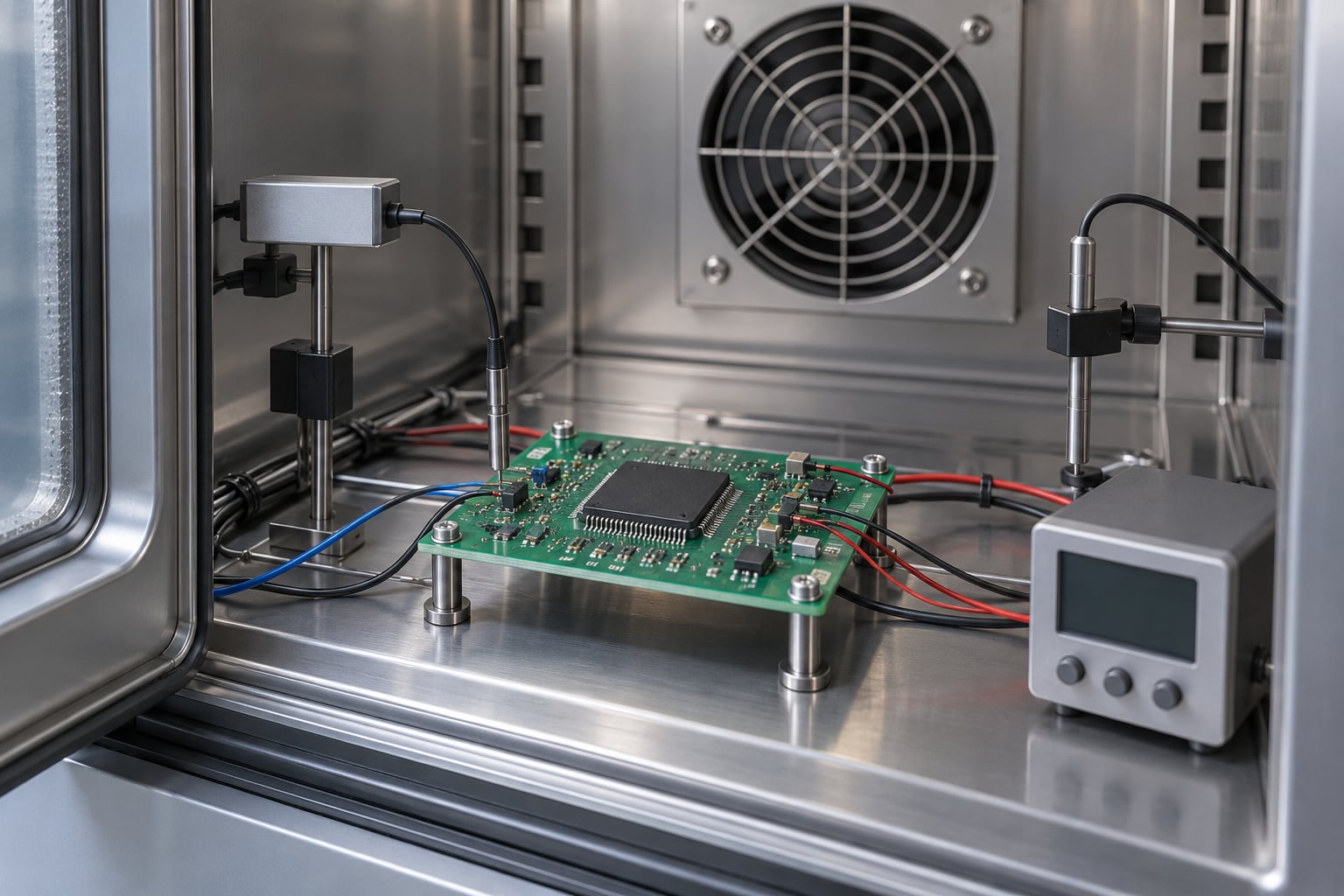
- Load into the chamber. Boards are loaded into a forced-air or inert-gas chamber and the chamber ramps to the target temperature.
- Ramp, soak and monitor. The chamber reaches setpoint, the supply comes up at the elevated voltage, and the tester records current and voltage for the full soak period.
- Cool down and unload. The chamber ramps back to ambient before the boards are handled, which avoids thermal shock to packages and bonds.
- Final test and binning. Devices are retested at room temperature, compared against their pre-burn baseline, and sorted into grade bins. Rejects go to failure analysis.
- Ship and record. Surviving devices ship with a record of their lot, board, conditions and results, which is what a customer audit asks for.
There are two important variants of that flow. Wafer-level burn in stresses dies while they are still on the wafer, before packaging, which is cheaper per device and catches front-end defects. The cost is that it cannot stress the assembly, so it misses bond and package problems entirely. Known good die is the middle path: wafer-level stress first, then only good dies get packaged, which is common where package cost dominates.
Board-level burn in is the other alternative. Assembled boards or modules go into the chamber instead of bare devices, which exercises the real power delivery path and is standard in telecom and datacom hardware. It finds system-level problems that bare-die screening cannot, at the price of less diagnostic clarity when something fails.
What Data and Reliability Metrics Are Collected?

A burn-in run that produces no data was a waste of chamber time. These are the numbers that come out of one.
- Failure rate per lot. The fraction of devices that failed during soak, tracked over time. A rising trend usually points at a process or assembly shift, not at the parts themselves.
- Escape rate. The fraction of burned-in devices that still fail soon after, typically in final test or in the field. It is the honest measure of how well the screen is working.
- Time to failure. When devices fail and at what point in the soak. Failures clustering early suggest gross assembly defects; a later cluster points at a slower wear mechanism.
- Parameter shift. Change in leakage, timing or drive current between the pre-burn baseline and the post-burn retest, against the allowed drift band.
- Activation energy. Derived, not measured directly. Running the same stress at two temperatures and comparing failure times gives a value that tells you how far the acceleration can be trusted.
- Accelerated lifetime. Projected life at the intended use temperature, from the Arrhenius relationship. Useful for planning, dangerous as a guarantee, because the projection assumes one activation energy and no change of mechanism.
That last caveat is the one to keep in view. Accelerated lifetime numbers are models built on assumed activation energies and assumed that the dominant mechanism does not switch as conditions change. They are fine for comparing processes and flagging lots. They are not a warranty, and no respectable reliability engineer treats them as one.
How Do Engineers Decide Whether Burn In Is Necessary?
Burn in is a tool, not a ritual, and the decision comes down to a few concrete questions.
- What happens if a field failure occurs? Automotive, medical, aerospace and defence applications have field failure costs that make screening cheap by comparison. Consumer volume products usually do not.
- What is the failure history? If previous lots on this process showed a measurable early failure rate, burn in has demonstrated value. If the escape rate is already near zero, another 500 hours buys little.
- How mature is the process? Newly qualified nodes and new package types have unknown mechanism populations. That is exactly when burn in pays for itself.
- What is the thermal headroom? The stress has to stay inside what the design can survive. Ask the design team for the maximum rated conditions before specifying a setpoint.
- What does it cost? Burn in consumes chamber capacity for hours or days, and rejected material is scrapped. On a large lot this is a real line-throughput decision, not a rounding error.
- What else could catch the same defects? Improved wafer sort coverage, better package stress testing, tightened assembly controls, or a known-good-die flow can remove some of the need.
One practitioner worry deserves a straight answer: yes, burn in can damage good parts if it is over-driven. Pushing voltage or temperature past the design’s rated maximum can create hot carrier damage and oxide stress in devices that would have shipped fine. The margin between aggressive screening and overstress is a specification question, and the specification should come from the design, not from a copied recipe.
Forum discussion on the topic tends to converge on the same two complaints, time and equipment. A long soak ties up chamber slots that a factory also needs for qualification work, and burn-in testers need substantial pattern memory to hold pre-computed patterns, which puts them out of reach for smaller labs. Both are real, and both push teams toward shorter, smarter conditions rather than longer ones.
Frequently Asked Questions
What is a burn-in test for semiconductors?
A burn-in test is a reliability screening process in which finished semiconductor devices are held at elevated temperature, usually with elevated supply voltage and steady current, for hours to days. The stress makes devices carrying manufacturing defects fail on the test floor instead of in a customer’s product. Devices that survive are binned and shipped.
What is the purpose of burn-in testing?
The purpose is to remove early-life failures before shipment. Semiconductor defects follow a bathtub curve, with a high failure rate early in life that drops sharply once the weak population is gone. Burn in accelerates that early phase, exposing electromigration, weak wire bonds, dielectric leakage and hot carrier damage while the parts are still under factory control.
What is the difference between burn-in testing and HTOL testing?
Burn in screens individual production units for early failures, usually at temperatures above normal use and often above rated supply voltage. HTOL qualifies a design, running a small number of samples for around 1000 hours at a defined high temperature to prove long-term reliability. One protects a shipment, the other proves a design.
What is burn testing?
Burn testing is an informal and older synonym for burn in, still used in some specifications and supplier documentation. Be careful with the search results: burn-in in displays means a permanent image ghost caused by static pixels, a completely different physical phenomenon with nothing to do with semiconductor reliability screening.
How long does burn-in testing take and at what temperature?
Common production screens run 24 to 100 hours at chamber setpoints between 85 °C and 150 °C, with the supply driven to 1.1 to 1.3 times rated. High-reliability programmes run far longer, up to 1000 hours, and several conditions in parallel. Duration is set by the mechanism being targeted and by how much chamber capacity the line can spare.
Does burn-in testing damage chips that would otherwise work?
It can, if the stress exceeds the design’s rated limits. Driving voltage or temperature past what the junction and gate oxide can hold causes hot carrier injection and time-dependent dielectric breakdown, which is real damage rather than screening. Safe conditions come from the design team’s ratings, not from a generic recipe copied between programs.
Conclusion: Start With the Device Reliability Risk
Burn in testing for semiconductors is worth doing when a field failure would cost more than the hours of chamber time it takes to find it, and when your process or package has a demonstrated population of early-life defects. It is not worth doing by reflex, at temperatures copied from a handbook, on a mature process that has never shown an escape rate worth worrying about.
Start with the risk. Identify which failure mechanisms your product is actually exposed to, pick the stress method that reaches them fastest, then validate the conditions against the design’s own ratings so you screen rather than damage. Treat the resulting data as a way to see your process, not as a lifetime guarantee, and keep the qualification work separate from the production screen so neither one gets substituted for the other.