Chip packaging is the back-end process that turns a fragile silicon die cut from a wafer into a finished, mountable component. The die gets attached to a leadframe or substrate, wired or bumped to external terminals, sealed in molding compound, trimmed, marked and electrically tested, so the part can be handled, shipped and soldered onto a board.
Understanding how chip packaging works matters if you design hardware, specify parts or just want to know what happens between “the wafer is finished” and “the part is on my board.” Here is the whole flow, step by step, followed by the package types, the cost drivers and where modern 3D stacking fits in.
Table of Contents
- What Is Chip Packaging and Why Does It Matter?
- How chip packaging works: the four jobs it does
- What Happens Between the Wafer and the Finished Part?
- How the Wafer Is Prepared for Packaging
- How the Die Is Attached to the Package
- How Electrical Connections Are Made
- Wire bonding still does most of the connecting
- Flip chip moves the connection to the underside of the die
- Copper clip and hybrid bonding shorten the path further
- How the Package Is Protected and Finished
- How a Packaged Chip Is Tested
- What Are the Main Chip Package Types?
- What Determines Packaging Cost and Performance?
- Frequently Asked Questions
- What is the first step in chip packaging?
- What is the difference between chip packaging and PCB assembly?
- Why are bump connections used instead of wire bonding?
- How is a packaged chip tested before shipment?
- Does chip packaging protect the die from heat?
- How do engineers choose between QFP, QFN and BGA packages?
- Key Takeaways
What Is Chip Packaging and Why Does It Matter?
A bare die is a few millimetres of silicon with bond pads measured in microns. It will crack if you look at it wrong, it has no connector, and nobody can pick it up with a pick and place machine. Packaging exists to fix all three problems.
How chip packaging works: the four jobs it does
- Mechanical protection. The die is small and brittle, so the package carries the shock of handling, shipping, soldering and board flex.
- Electrical connection. Microscopic pads on the die are tied to package leads or balls that a board assembler can actually solder.
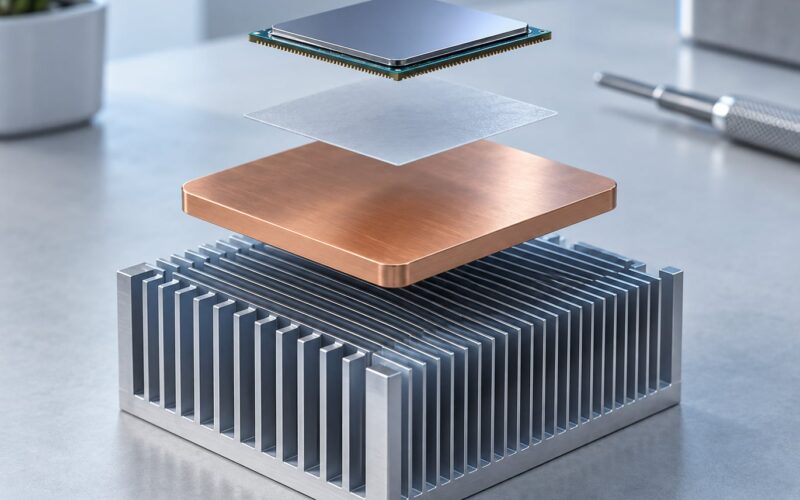
- Thermal path. A deliberate route for heat to leave the die, through the attach material, substrate or leadframe, out to the board copper or a heat spreader.
- Test and traceability. A place to run final electrical test, and a marking surface for the lot code, date code and part number.
Two words get confused here. Wafer fabrication is the front end: growing the crystal, building transistors in silicon. Assembly and test is the back end: everything described here, sometimes called packaging, assembly and test, or AT.
Engineers often talk about three levels of chip packaging. Die level packages sit right on the die for close-in decoupling and filtering. Package level is the single-die molded component such as a QFN or BGA. Board level is a module or board where several packaged parts are assembled together, which is a different craft from IC packaging.
What Happens Between the Wafer and the Finished Part?
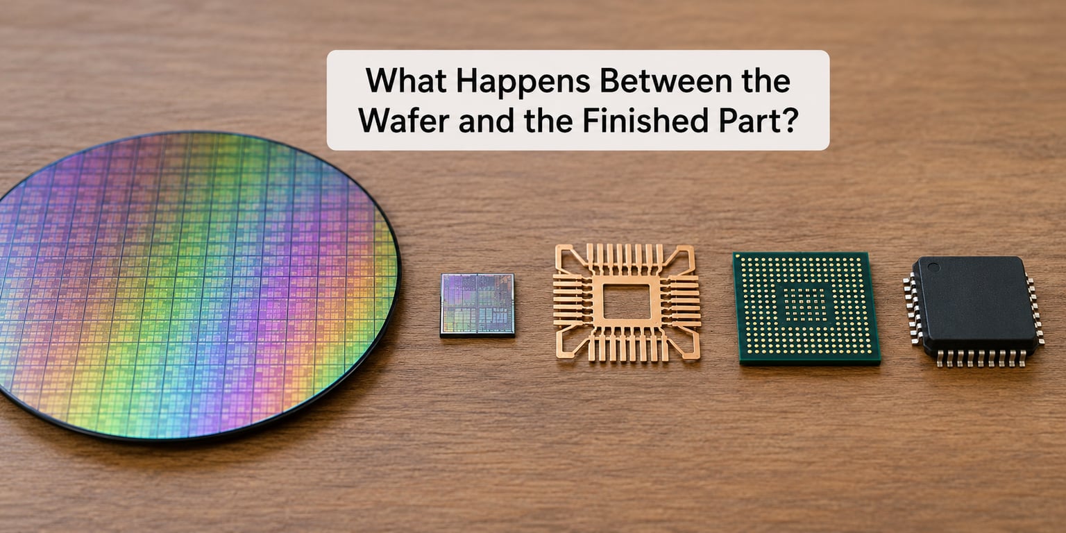
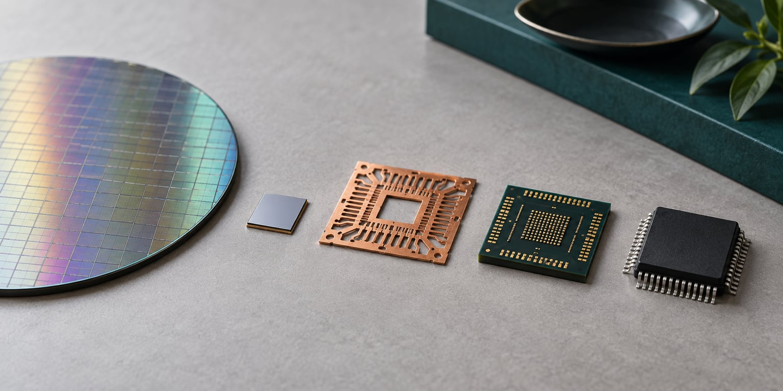
Ten steps take a wafer to a binned, marked, tested part. The order matters: you cannot bond a wire to a die you have not thinned, and you cannot mold a package whose die has not been attached.
| Step | What happens | Why it matters | Common defect |
|---|---|---|---|
| 1. Wafer probe (wafer sort) | A probe card touches each die’s pads and runs a fast electrical test | Confirms a known good die before money is spent packaging it | Probe marks that crack pads |
| 2. Wafer grinding | The back of the wafer is ground down to a target thickness | Thin wafers cut faster and give a better heat path | Wafer warp and die edge chipping |
| 3. Wafer mounting | The thinned wafer is stuck to a rigid carrier film or frame | Prevents breakage once the wafer is too thin to handle | Carrier peel damage to the die back |
| 4. Dicing (singulation) | A saw or laser cuts the wafer into individual dies | Separates each die while keeping edges clean | Dicing cracks, edge chipping |
| 5. Die attach | The die is bonded to a leadframe paddle or package substrate | Fixes the die in place and starts the heat path | Die tilt, voids in the attach layer |
| 6. Interconnect | Bond wires, solder bumps, copper clips or hybrid bonds join die pads to terminals | Creates the electrical path out of the silicon | Wire lift, open solder joints |
| 7. Molding | Epoxy molding compound is transfer-molded over the assembly and cured | Seals and protects the die, adds stiffness | Delamination, mold flash, “popcorn” cracks |
| 8. Trim and form | Excess leadframe is cut away and leads bent into their final shape | Separates parts and makes them board-mountable | Bent or nicked leads |
| 9. Marking | A laser or inkjet prints the part number, lot code and date code | Traceability back to the wafer lot and process conditions | Illegible or misprinted code |
| 10. Final test | A handler places the part in a socket, runs full electrical test, bins it | Only good parts ship; binning grades speed and grade | Socket damage, handler mis-pick |
How the Wafer Is Prepared for Packaging
Wafer probing comes first. A probe card with hundreds of microscopic needles lands on the die pads, and the tester runs a shortened version of the final test. Dies that fail here never get packaged, which is the whole point: packaging a bad die costs far more than probing one.
Most dies ship in a standard 300 mm wafer roughly 700 micrometres thick, and a moulded package does not want that much silicon in it. Backgrinding removes material from the back until the wafer hits a specified thickness, sometimes down to a few hundred micrometres for a thin package.
Grinding leaves the wafer flexible and fragile, so it gets laminated to a carrier film or mounted on a rigid frame. From there the dicing saw or laser cuts the streets between dies, and each die is singulated off the frame and cleaned of grinding residue.
Inspections happen here rather than at the end. Automatic optical inspection looks for chips, cracks and contamination, and dies that are used in a high-cost package may go through a cross-section check to confirm backside grind quality. In parallel, the package itself is prepared: leadframes arrive plated, and organic substrates or silicon interposers are shipped pre-routed and surface-treated.
How the Die Is Attached to the Package
Die attach is the step that decides where heat goes. The die has to be held flat and rigid for the bonder that follows, and it has to be stuck down well enough to survive reflow and temperature cycling years later.
Four methods cover almost everything. Die attach film is a pre-formed adhesive film placed by a pick-and-place machine and cured in a convection oven, common in leadframe packages. Solder attaches the die to the leadframe paddle or a ceramic substrate and is the default for power devices, where the die itself is often a deliberate thermal pad exposed to the outside of the package. Conductive adhesive carries both heat and a ground connection where solder would be too rigid. Direct bonding fuses copper to copper with no filler, used where the interconnect and the thermal path both have to be as short and as conductive as possible.
The three requirements to check against: heat must leave the die, stress on the die must stay low, and the attach material must be electrically compatible with what sits above and below it.
How Electrical Connections Are Made
Once the die is down, the pads on its surface have to reach terminals outside the package. Two methods do most of the world’s work, and the choice is a straight trade between connection density and cost.
| Parameter | Wire bonding | Flip chip |
|---|---|---|
| Typical pad pitch | Coarse to moderate; limited by wire loop and tool | Fine; driven by bump pitch and substrate routing |
| Interconnect length | Wire loops, hundreds of micrometres to millimetres | Short, on the order of the bump height |
| Parasitics | Higher resistance and inductance per connection | Lower, better for high-speed signals |
| Thermal and mechanical | Wire adds a soft, compliant element; strain relief is a design task | Stiffer joint; underfill usually required |
| Assembly cost | Low, mature, high throughput | Higher, needs bump formation and careful substrate control |
| Typical use | Low and mid pin count, analog, MCUs, power | High pin count, mobile and compute SoCs, memory |
Wire bonding still does most of the connecting
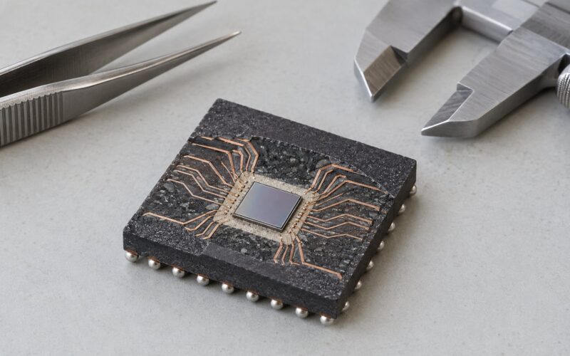
Gold, copper or aluminium wire, typically 15 to 500 micrometres thick, is drawn from a capillary tool. In thermosonic ball bonding, a free-air ball is formed with an electronic flame-off, pressed onto the pad with force and ultrasonic energy, and the wire is then looped and stitch-bonded to the lead. The loop shape is a deliberate design parameter: it is the strain relief that stops thermal cycling from working the bond apart.
Flip chip moves the connection to the underside of the die
Here the bumps are formed on the die itself, by plating, evaporation or printing solder paste, and reflowed. The die is then flipped, aligned to the substrate and bonded in one reflow step that makes every connection at once. A capillary or a stencil dispenses underfill into the gap and cures it, which stiffens the joint and spreads stress across the whole area.
Copper clip and hybrid bonding shorten the path further
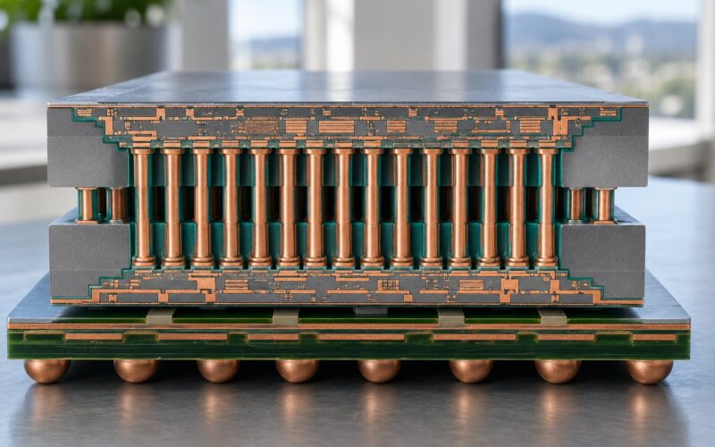
Copper clip bonding replaces the wire loop with a formed solid copper element, shortening the path and removing the loop as a failure mode. Hybrid bonding goes further: two surfaces are polished flat and brought into contact at high temperature and pressure so copper and oxide fuse directly, with no solder in the joint at all. That is the interconnect behind 3D stacked memory and logic.
How the Package Is Protected and Finished
Most packages are transfer molded: solid epoxy molding compound, a mixture of resin, filler and hardener, is pressed from a pot through a mould cavity in a few seconds, surrounding the die and wires on all sides. It is fast, it fills thin gaps without voids, and it locks the wire loops in place. The compound is then cured at high temperature for one to several hours, depending on the formulation.
Where you need a metal rather than a plastic shell, a lid or heat spreader attaches instead, and cavity packages are sealed or given an underfill for moisture resistance. That resistance is graded by moisture sensitivity level in the JEDEC standard, which tells the board assembler how long the part can sit on the shelf before baking or reflow, and how carefully it must be handled.
After cure, the assembly goes through trim and form. A punch or saw cuts the leadframe webs apart, then a former bends the leads to the right pitch, length and coplanarity. Marking follows, and for most fabs it is a laser that marks the top surface without touching the die.
The common damage modes show up in predictable places: delamination when compound does not bond to the leadframe, mold flash when compound escapes the cavity, and the “popcorn” effect, where trapped moisture inside a moisture-sensitive package expands during reflow and cracks the part apart.
How a Packaged Chip Is Tested
Testing happens three times over the life of a part, and each one proves something different.
Wafer probe runs before singulation and produces the known good die, or KGD, that the rest of the process assumes. Final test happens after marking: a handler picks the part, places it in a test socket, runs the full electrical test at temperature, and puts it in a bin by performance grade. Final test is where speed binning happens, which is why two parts with the same part number can behave differently.
Reliability qualification uses sample parts rather than every part. A wire pull test measures bond strength in force, a ball shear test measures the solder joint on flip-chip parts, X-ray inspection finds voids and shorts under the package, and AOI checks the surface and lead coplanarity. Worth remembering that X-ray shows geometry, not function, and AOI finds defects the die cannot see.
For parts with early-life failure risk, burn-in holds devices at elevated voltage and temperature for hours, sometimes days, so infant mortality shows up before shipping rather than in the field. Qualification standards such as JEDEC JESD22 and AEC-Q100 govern how these samples are chosen and what a part must survive to be called qualified.
What Are the Main Chip Package Types?
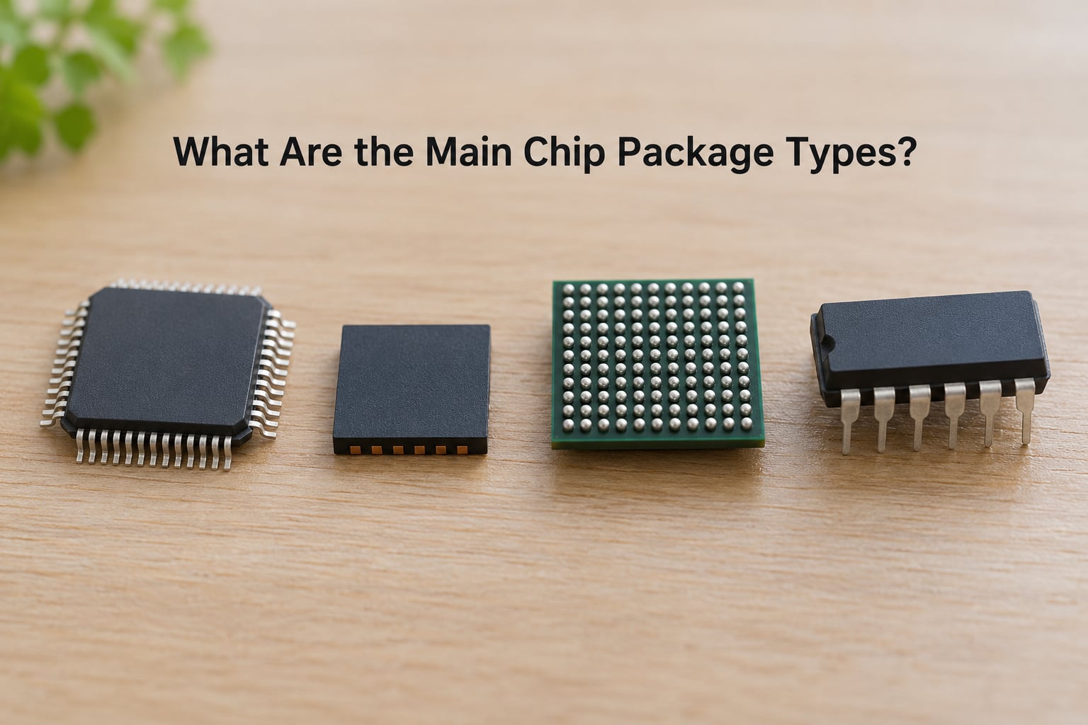
One mix-up worth clearing up early: BGA and flip chip are not the same thing. BGA describes the external terminals, a ball grid on the underside. Flip chip describes the internal connection from die to substrate. A BGA is often flip chip, but a wire-bonded BGA exists, and a QFN is often flip chip while having no balls at all.
| Package | Structure | Connection to board | Typical use |
|---|---|---|---|
| DIP (through-hole) | Molded body, pins pass through | Through-hole insertion | Prototyping, legacy, high-voltage isolation |
| QFP | Molded body, gull-wing leads on four sides | Surface-mount, perimeter | Mid pin count, easy inspection, cost-sensitive designs |
| QFN | Flat no-lead body, small pads underneath | Surface-mount, perimeter plus exposed pad | Space-constrained, good thermal path, often flip chip |
| BGA | Substrate body, array of balls underneath | Surface-mount, area array | High pin count, mobile, processors |
| LGA | Substrate body, flat contact pads | Surface-mount, area array | Very high pin count, sockets and low profile |
| Flip-chip | Bumped die bonded face-down, underfilled | Depends on carrier: BGA, LGA, QFN | Shortest electrical path, RF and high-speed |
| SiP / stacked | Several dies in one package, or dies stacked vertically | Carrier-dependent | Integration where one monolithic die is impractical |
What Determines Packaging Cost and Performance?
Packaging cost tracks complexity, and complexity tracks connection count. Bigger dies need bigger leadframes and substrates. Higher I/O counts force finer pitch, which means better substrate routing, tighter alignment and more expensive inspection. A wire-bonded QFP on a stamped copper leadframe and a flip-chip BGA on a build-up organic substrate are not the same product with different labels.
Thermal requirements push the other way. A part that has to shed real heat may need a heavier copper clip, an exposed pad, a die attached with solder instead of adhesive, or a lid on top of the compound. Each of those adds a process step and a failure mode to check.
Volume matters more than people expect, because every one of these steps has setup cost that amortises across the lot, and testing cost scales with test time per part rather than with unit cost. Test complexity is another driver: a part needing burn-in or tested at multiple temperatures takes far longer on the handler than one that gets a single fast pass.
Cycle time from wafer-out to a binned part is typically a few days to a few weeks, depending on how much of the flow is at a foundry versus an independent assembler. That is also where advanced packaging changes the picture. 2.5D builds place dies side by side on a silicon interposer such as TSMC’s CoWoS, 3D stacking bonds dies face to face, and HBM stacks join many memory dies vertically with hybrid bonding. Fewer transistors per die, more performance per package, and far more interconnect per square millimetre.
So who does the work? Foundries such as TSMC do a lot of their own packaging, including CoWoS, while independent OSATs such as Amkor, ASE and JCET handle the bulk of volume assembly and test for companies that do not run their own back end. The answer to “does TSMC do chip packaging” is yes, and it is also true that most packages on the planet were put together by someone else.
Frequently Asked Questions
What is the first step in chip packaging?
The first step is wafer probing, also called wafer sort, where a probe card lands on each die and runs a short electrical test before anything is cut or bonded. Dies that fail are mapped and dropped, so only known good die goes into packaging. This saves a great deal of money, because a package that has already been molded around a bad die is scrap.
What is the difference between chip packaging and PCB assembly?
Chip packaging surrounds the die to make a mountable component, ending when the part is tested, binned and marked. PCB assembly happens later: the packaged components are placed on a board, soldered, and inspected. Packaging connects the die to a component; board assembly connects components to each other through copper tracks.
Why are bump connections used instead of wire bonding?
Bumps shorten the electrical path dramatically, because the connection height is a fraction of a wire loop. That cuts resistance, inductance and signal delay, which matters at high frequencies and high data rates. Bumps also support much finer pitch, letting one die reach far more I/O than wire loops of practical size allow.
How is a packaged chip tested before shipment?
Final test puts each part in a socket on a handler, runs the full electrical test at temperature, and bins it by performance grade. Sample parts from every lot also go through reliability checks such as wire pull, ball shear, X-ray and AOI. Parts with early-life failure risk get burn-in before they are released.
Does chip packaging protect the die from heat?
Partly, and it is better to think of the package as a controlled heat path rather than a shield. The die attach material, paddle or substrate, and any lid or exposed pad form a route for heat to reach the board or a heat spreader. Good design keeps that path short; a package cannot remove heat that never has anywhere to go.
How do engineers choose between QFP, QFN and BGA packages?
They start with I/O count, then pitch, then what the board can do. QFP suits mid pin counts because its leads are visible and easy to inspect. QFN shrinks the footprint and gives a good thermal path for tight designs. BGA takes the highest pin counts but needs X-ray inspection and careful board layout for escape routing.
Key Takeaways
How chip packaging works comes down to one ordered flow: probe, grind, mount, dice, attach, interconnect, mold, trim and form, mark, test. Every step after wafer probe assumes the die already passed an electrical test, and every step has one defect it is responsible for.
If you are specifying a package, start by pinning down five things: the die size, the number and pitch of connections, the heat the part has to shed, the package format your board can assemble, and how thoroughly it must be tested. Get those right and the package family usually picks itself. Get the thermal or pin count wrong and no amount of clever interconnect saves it.