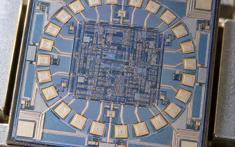
Corner analysis in chip design is the practice of running a design against the extreme combinations of process, voltage and temperature it must survive, rather than trusting timing at one nominal point. Setup timing is worst at the slow-process, low-voltage, high-temperature corner. Hold timing is worst at the fast-process, high-voltage, low-temperature corner. No single corner is worst for everything, which is the whole reason the work exists.
Below is the practical version: what a corner actually is, how it differs from a mode, which corners each check cares about, and how to work through a failing corner without over-designing the block.
Table of Contents
- What Is Corner Analysis in Chip Design?
- The standard corner naming convention
- Why Corners Matter for Timing, Power, and Reliability
- What Is the Difference Between a Corner, a Mode, and a Scenario?
- Which Corners Does Static Timing Analysis Check?
- How Do You Perform Corner Analysis in Chip Design?
- Step 1: Start from the constraints, not the corner list
- Step 2: Load characterised libraries for the right corners
- Step 3: Define the scenarios once, in MMMC
- Step 4: Pick the corners, then validate the pick
- Step 5: Isolate the limiting condition per path
- Step 6: Close the violation and rerun
- What Results Should You Review Across Corners?
- Why Does Corner Analysis Fail in Real Chips?
- How Do You Fix Timing Failures That Appear at One Corner?
- Frequently Asked Questions
- Is corner analysis still necessary at advanced process nodes?
- What corner is usually worst for setup timing?
- Why can a path pass at one temperature and fail at another?
- How many timing corners should a chip design analyze?
- Does corner analysis include dynamic power and signal noise?
- Should engineers fix every path that has negative slack?
- Conclusion: What to Do First
What Is Corner Analysis in Chip Design?
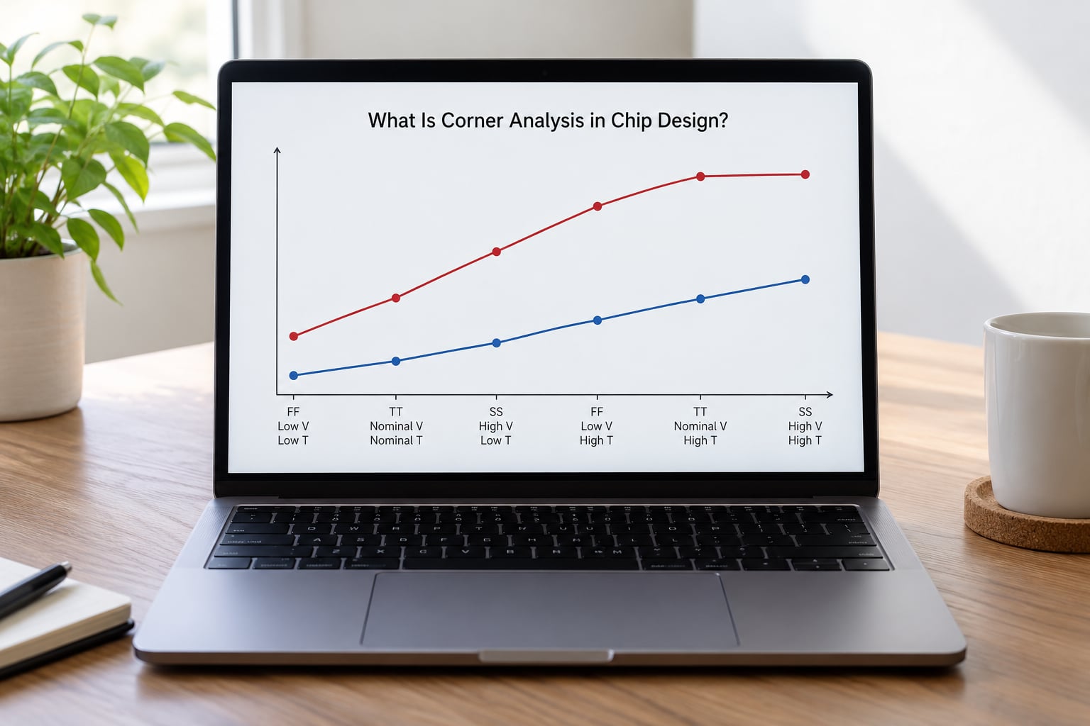
A corner is one named operating point on three axes at once: process speed, supply voltage, and junction temperature. Timing analysis uses a characterised library of cell delays at each of those points, so choosing a corner is really choosing which set of numbers the tool computes arrival and required times from.
Corners exist because two chips cut on the same wafer, running the same firmware, at the same voltage, are not electrically identical. Process variation moves transistor speed and threshold voltage. Voltage and temperature then push those transistors around further. A single nominal delay is just one point in a cloud.
The standard corner naming convention
The letters encode process speed and the voltage and temperature that typically travel with it. The first letter is the process condition the foundry uses for that bin.
| Corner | Process | Voltage | Temperature | Typical use |
|---|---|---|---|---|
| SS | Slow | Low (nominal minus tolerance) | High | Setup timing worst case |
| TT | Typical | Nominal | Ambient or mid-range | Power, average timing, exploration |
| FF | Fast | High | Low | Hold timing worst case, race checks |
| FS | Fast | Nominal | High | Hold with hot silicon, leakage-driven checks |
| SF | Slow | Nominal | Low | Cold-start behaviour, margin opposite to FS |
One table is not enough on its own. A real signoff list adds voltage domains, aging states, and process splits, which is where the corner count starts to climb.
Why Corners Matter for Timing, Power, and Reliability
Process sets transistor speed and threshold voltage. A slow bin loses drive strength and leakage drops; a fast bin gains both. The delay of a given gate at the slow bin can be substantially longer than at the fast bin, and a library hides most of that spread behind timing arcs it expects you to analyse at multiple points.
Voltage does the same thing in the same direction as speed: less headroom means less current into the load capacitance, so every stage is slower. Higher voltage means faster transitions and more dynamic power, and in a low-voltage design near threshold voltage the sensitivity is much sharper than the headline voltage number suggests. That is why corner analysis in chip design treats voltage as a real axis rather than a rounding error.
Temperature mostly degrades mobility and raises leakage. Hot silicon is slower and thirstier at the same time, which is the unkind combination. It also shifts what reliability analyses see, since electromigration current density and IR drop both move with temperature and activity.
Aging is treated as an extra dimension in libraries that model it, often as a derated or separately characterised timing state representing several years of bias-temperature-bias and hot-carrier-injection stress. A path that closes at the fresh-library slow corner can drift as the transistor ages, so a corner set with no aging state is only describing week-one silicon.
What Is the Difference Between a Corner, a Mode, and a Scenario?
This is where most confusion in the first year of STA comes from. A mode is a functional condition, such as functional operation, scan shift, scan capture, test, or a low-power state. A corner is a PVT point. A scenario is the name for one pairing of a mode with a corner, plus any scenario-specific settings.
| Corner | Mode | Scenario | |
|---|---|---|---|
| Question it answers | Under what electrical conditions? | Under what functional conditions? | Which mode is checked at which condition? |
| Examples | SS, FF, FS, SF with named voltage and temperature | Functional, scan shift, scan capture, test, sleep | scan capture at SS for setup, scan shift at FF for hold |
| Set by | Foundry and library views | Design intent and DFT architecture | Both, plus tool flow configuration |
| Typical count | Dozens to hundreds | Few | The cross product, which is the expensive part |
A mixed-mode example: a scan chain flop is checked for hold in scan shift mode at FF, because that is when a shifted value races the shift clock. The same flop is checked for setup in functional mode at SS, because that is the condition that governs capture timing on real data. The mode and the corner are independent choices, and swapping either one changes the answer.
Multi-mode multi-corner, or MMMC, is simply the tool flow that defines all those pairings once and runs them as a set. The reason signoff does not run every mode against every corner is that the full cross product grows multiplicatively and most pairings are meaningless, such as scan shift at a high-temperature high-voltage corner with aging applied.
Which Corners Does Static Timing Analysis Check?
Setup and hold are checked at opposite corners because the failure mechanisms are opposite. Setup fails when the data path is too slow relative to the capture clock, so the slow bin, low voltage and high temperature stack up on the same side. Hold fails when the data arrives too early at the capture flop, so the fast bin, high voltage and low temperature are the stressing conditions.
Not all corners are used the same way. Maximum transition and maximum capacitance checks, slew degradation, often appear at fast corners where drive is highest. Minimum pulse width checks pair high temperature with the slow process bin. Aging, when modelled, is usually applied as a modified library or derate on top of a chosen corner rather than as an axis you sweep separately.
On-chip variation sits underneath all of this. A PVT corner describes the whole die as one condition, but two cells at opposite ends of the same die are not identical. OCV applies a distance and depth-dependent derate so that a launch cell at the far side of the core gets a pessimistic delay relative to a nearby capture cell. POCV expresses that same effect as a statistical sigma rather than a fixed percentage.
That is why running every PVT corner still does not replace variation margin. The corners cover die-to-die, wafer-to-wafer and lot-to-lot spread. The derate covers intra-die spread, which is a separate axis entirely.
Signoff libraries also carry more views than any engineer reviews by hand. A foundry may qualify a dozen process bins, several voltage taps, and multiple temperatures per voltage rail. The flow picks a subset for routine runs and keeps the rest for diagnosis.
How Do You Perform Corner Analysis in Chip Design?
Step 1: Start from the constraints, not the corner list
Read the SDC first. Clock definitions, generated clock waveforms, input and output delays, and case analysis tell you which scenarios are even meaningful. Many corner failures trace back to a waveform or uncertainty value that was never written down properly.
Step 2: Load characterised libraries for the right corners
Map every voltage domain to its operating range, then pair those with the temperature range from the product specification. In chip design this includes the cold-start or ambient floor, not just the hot operating ceiling. Check that the library views you loaded match the corners you intend to analyse, because a mismatched or stale view set quietly invalidates everything downstream.
Step 3: Define the scenarios once, in MMMC
Set up functional, scan and any test or low-power modes, and assign each the corner subsets it needs. Doing this in the flow rather than by hand keeps the scenario list identical across synthesis, place and route, and signoff, which matters when engineers and scripts both touch the same database.
Step 4: Pick the corners, then validate the pick
A useful habit is to run one broad sweep early in the project and compare it against the smaller routine set. That converts an assumption about which corner is worst into a checked result. On one thread in r/chipdesign a team described running around 60 corners with voltages spanning roughly 0.5V to 0.9V and temperatures from -40C to +150C, using on-die process monitors to see which conditions real parts actually visit.
Step 5: Isolate the limiting condition per path
For any violating endpoint, look at which scenario, which corner and which clock dominate. PrimeTime, Tempus and the other mainstream engines all report this, and the fastest debugging path is usually to open the worst path in the corner that produced the worst slack, not in the corner you expected.
Step 6: Close the violation and rerun
Fix the cause, then rerun every affected scenario. A change that helps setup at SS can easily cost you hold at FF, so closing one corner and declaring victory is how designs slip through.
What Results Should You Review Across Corners?
| Check | Stressing corner | Why |
|---|---|---|
| Setup timing | SS, low voltage, high temperature | Longest data path against the capture edge |
| Hold timing | FF, high voltage, low temperature | Earliest data arrival races the capture edge |
| Max transition | Fast corners | High drive and low load produce the sharpest edges |
| Max capacitance | Slow corners | Weak drivers cannot charge large loads |
| IR drop and electromigration | Hot, low voltage, high activity | Resistance rises and current density concentrates |
| Aging and reliability | Slow process plus stress models | Transistor parameters shift over years |
Beyond the pass and fail flags, watch how the worst path changes identity across corners. If a different register-to-register path sets the critical path in every corner, your design is not balanced and your optimisation is chasing a moving target.
Watch setup and hold slack separately, and total negative slack alongside worst negative slack. A design with a small WNS and a large TNS usually needs structural work rather than one lucky buffer.
Look at slew and capacitance degradation because both feed the other metrics. Power is worst at the opposite end of the range from the setup corner, usually high temperature at the fast or typical process bin for dynamic power and the slow bin for leakage, so a single power report at TT hides both ends.
Why Does Corner Analysis Fail in Real Chips?
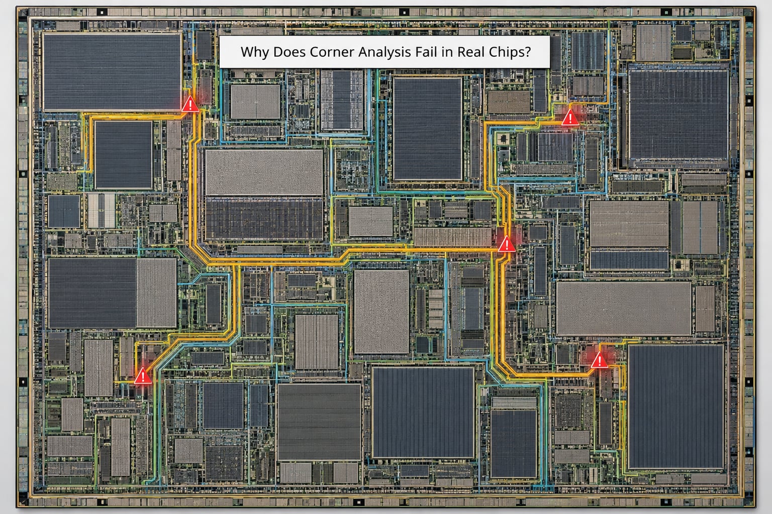
Incomplete corner sets are the first cause. A team fixes the corner that failed during implementation, ships, and finds the opposite check failing in silicon because the complementary corner was never in the routine set.
Constraint errors come next. A missing clock uncertainty, a generated clock modelled with the wrong duty cycle, or an output delay defined on the wrong port will produce corner results that look plausible and are wrong in the same way at every corner.
Then there is library mismatch. Loading a characterisation view for a different voltage tap or an older revision makes the corner label a lie, and the tool will not warn you because everything it was given was internally consistent.
On-chip variation gets dropped when the OCV or POCV file is missing or set to zero. Every corner looks clean, the paths are all positive, and the part still fails at speed.
MMMC setup errors are quieter still. Scan mode checked against functional corners or a test mode left out entirely removes real paths from the report without any warning that they stopped being analysed.
Finally, over-guardbanding. Padding every corner with large margin because a single case was once mysterious produces a design that is larger, slower and hotter than it needs to be. On the other side of the same forum thread, practitioners described the reluctance to move to purely statistical methods because those do not give a clean yes or no answer, so deterministic corners plus margin remain the practical default even when a distribution is more honest.
How Do You Fix Timing Failures That Appear at One Corner?
First, confirm the corner is real. Check whether the failing path is a true endpoint violation or a scan shift hold check that only exists because of how the chain is clocked, and confirm the derate file that is active matches the flow the project signs off with.
Second, compare the same path across corners. If the fix you are considering changes timing at SS but leaves FF untouched, you have found a fix that works for one check only. Cell swaps and buffer insertion behave this way often enough that it is worth reading the report across two corners before touching anything.
Third, fix the physical cause. Setup failures on a specific net usually mean drive, load, or wire length. Hold failures on short local paths usually mean excess delay in the launching logic or an over-buffered net.
Fourth, keep the design intent intact. Changing a clock-gating condition or a reset path to make a corner pass can break another mode that was previously clean, so check the scenario list rather than only the failing scenario.
Fifth, rerun the full affected set and compare against the broad sweep. If the routine corner set and the sweep disagree after the ECO, the routine set has a gap and that gap just cost you a respin.
Frequently Asked Questions
Is corner analysis still necessary at advanced process nodes?
Yes, and the job gets harder rather than easier. At 5nm-class nodes and below, voltage headroom shrinks, transistors sit closer to threshold voltage, and variation between neighbouring cells grows. That means delay changes more sharply across a small voltage range and on-chip variation matters more. The libraries also model aging and variation in finer detail, which means more realistic corner sets rather than fewer.
What corner is usually worst for setup timing?
The slow process corner combined with low voltage and high temperature, usually written SS. All three push the same way: less drive current into the load capacitance means a longer data path delay. Aging states and pessimistic on-chip variation derates can make the effective case worse than the raw corner name suggests, so reports often name a corner plus a derate file.
Why can a path pass at one temperature and fail at another?
Higher junction temperature reduces carrier mobility, so transistors switch more slowly and the same path delay grows. Leakage rises at the same time, which changes power and can shift which paths dominate. A path with only a few picoseconds of setup slack at room temperature can easily go negative at the hot operating limit, which is why ambient results are never a signoff substitute.
How many timing corners should a chip design analyze?
It depends on the product class and the constraint you are given. An IoT design may sign off on a small minimum set with margin. Automotive parts cover a wide range and are checked across the full specified span. Mobile and high-performance SoC teams have described signing off on hundreds of corners because of their own performance targets and compute cost. The right number is the smallest set proven to catch the true worst case.
Does corner analysis include dynamic power and signal noise?
In a complete flow it should. Power, IR drop, electromigration and signal integrity all shift with temperature, voltage and activity, and running them only at the typical corner tends to hide the worst case. The tools differ from timing engines, for example Voltus for power integrity and Calibre for physical verification, but they consume the same corner definitions, so the corner list should be built once and reused.
Should engineers fix every path that has negative slack?
Not in the order you would expect. Start with the worst negative slack and the paths feeding the largest total negative slack, since those usually share one root cause in drive or congestion. Isolated negative slack on a non-critical path can sometimes be handled by a constraint review rather than a physical change. What matters is that every endpoint reaches zero slack at the corner that stresses it.
Conclusion: What to Do First
Start by writing down the actual conditions your design has to meet: the process bins you were given, every voltage domain with its operating range, and the temperature floor and ceiling from the product specification. Nothing else in corner analysis is meaningful until those three lists are real.
Then check what is being reported. Confirm that timing is being run across a complete corner set rather than a single point, that the on-chip variation derate is loaded, and that both setup and hold reach zero slack at the corners that stress them.
If that is not true today, run one broad sweep against the routine set and compare. Corner analysis in chip design is mostly a discipline of keeping the reported worst case aligned with the real worst case, and 2026 foundry view sets and tool defaults make it easy to drift away from that without noticing.