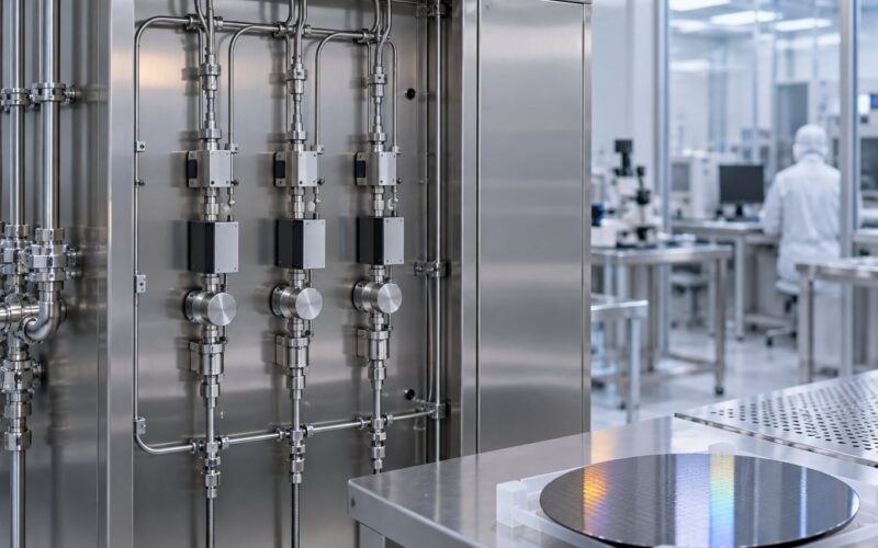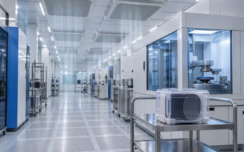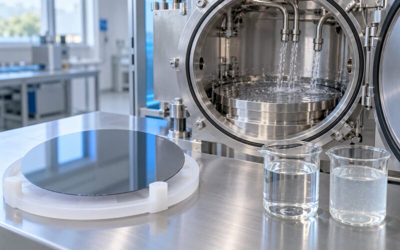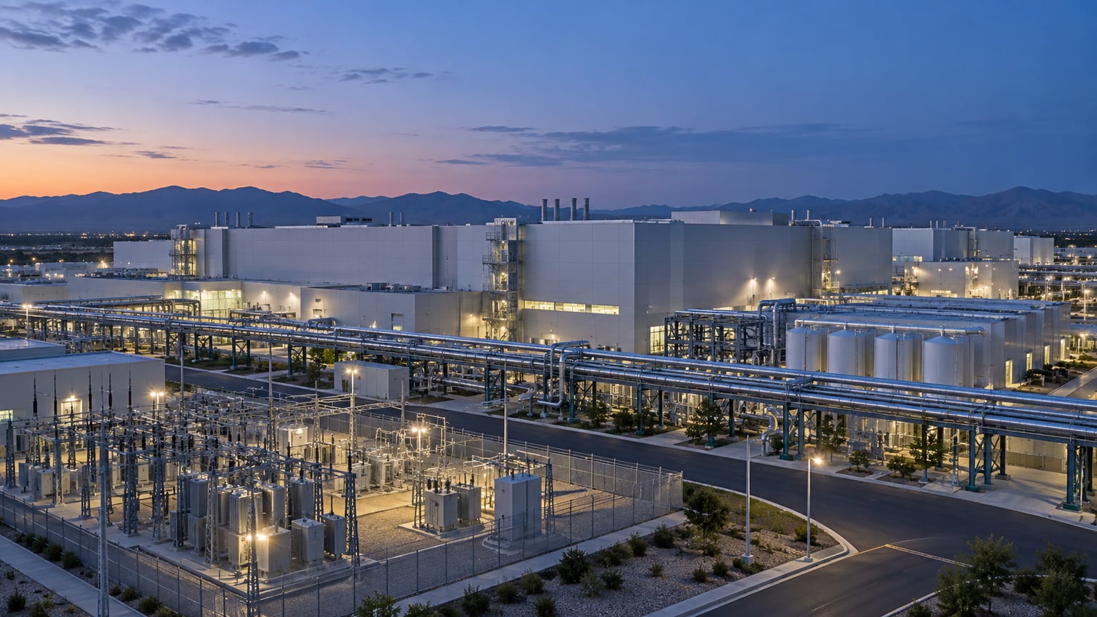
How much electricity does a semiconductor fab consume? A large 12-inch (300mm) fab draws roughly 100 megawatt-hours every hour, which is a continuous load of about 100 to 200 megawatts. In annual terms, a fab of that size consumes on the order of 1 terawatt-hour, comparable to what about 50,000 households use in a year. Leading-edge facilities running at high utilisation can exceed 200 MW once fully ramped.
That headline number gets quoted everywhere, and it is useful, but it flattens several different measurements into one. A facility’s peak demand in megawatts, its annual consumption in terawatt-hours, and its energy intensity per wafer in kWh/cm2 are three separate things that move independently. If you are comparing facilities, planning a grid interconnect, or arguing about whether chip manufacturing is genuinely energy-hungry, keeping those measures apart is most of the work.
Below is a breakdown using dated, attributed figures rather than round numbers pulled from a listicle.
Table of Contents
- How Much Electricity Does a Semiconductor Fab Consume?
- What Is the Typical Electricity Use of a Semiconductor Fab?
- What Uses the Most Electricity Inside a Fab?
- Process tools
- Cleanroom air handling
- Chillers and cooling water
- Compressed dry air and vacuum
- Ultra-pure water, chemicals and material handling
- Support buildings
- Why Do Fabs Have Such High Energy Needs?
- How Much Electricity Does One Wafer Consume?
- Why the 100 to 150 kWh per cm2 figure circulating online is wrong
- A worked example
- From wafer to die
- How Does Fab Energy Use Compare Across Technologies?
- What Factors Change a Fab’s Electricity Consumption?
- How Do Fabs Reduce Electricity Use?
- Efficiency at the HVAC and air handling level
- Tool-level power management
- Heat recovery
- Leak detection and compressed air
- Process and yield optimisation
- Powering strategy
- Frequently Asked Questions
- Do semiconductor fabs use a lot of water?
- Are semiconductor factories bad for the environment?
- How much electricity does an aluminum smelter use?
- How much of a country’s electricity does TSMC use?
- Who is TSMC’s biggest rival?
- How much energy will AI really consume?
- Conclusion
How Much Electricity Does a Semiconductor Fab Consume?
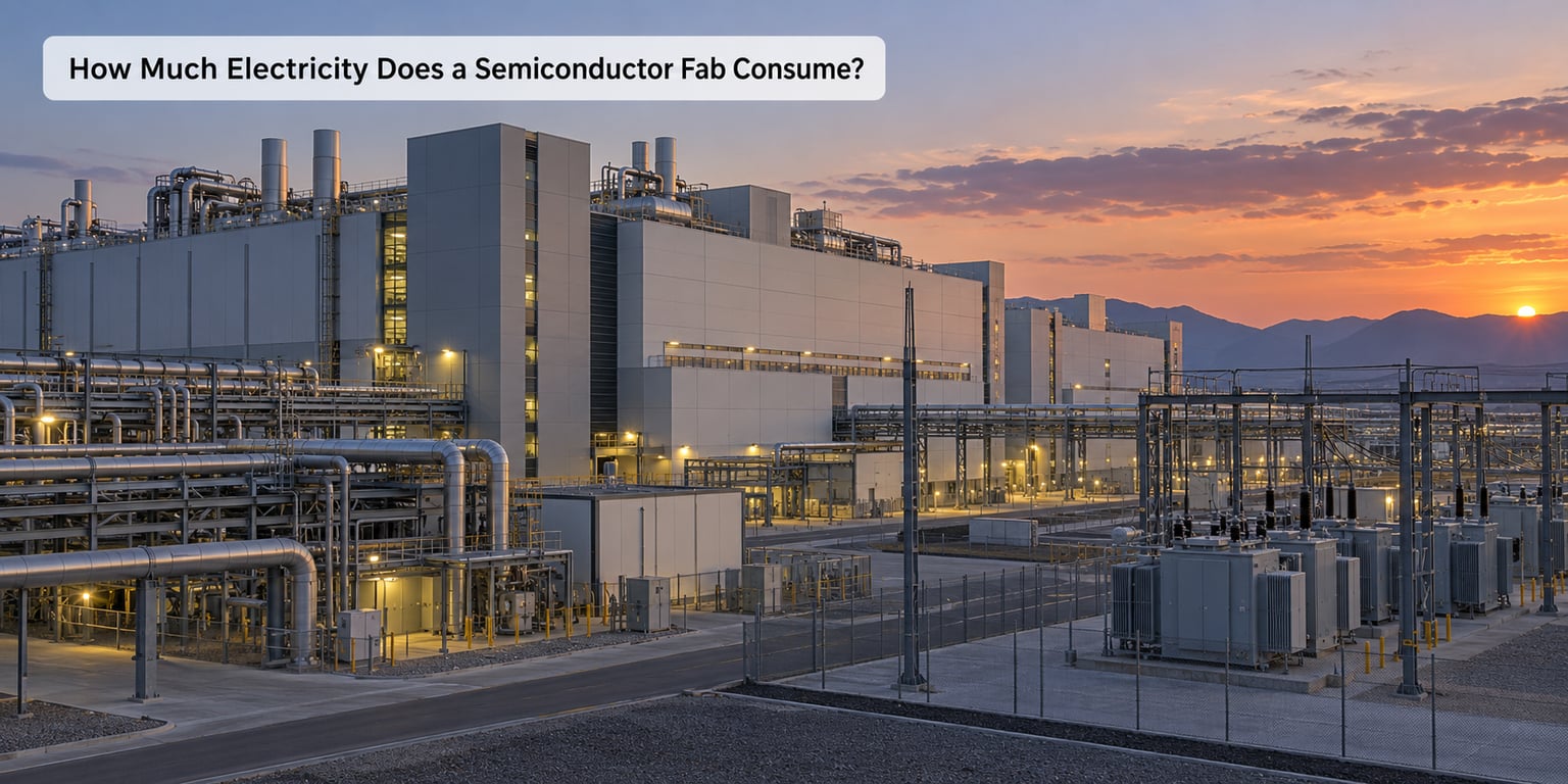
How much electricity a semiconductor fab consumes depends on wafer size, node, utilisation and cleanroom specification, but the short answer is this: a large 300mm fab runs on roughly 100 to 200 megawatts of continuous load, equal to about 100 to 200 megawatt-hours per hour, and somewhere around 1 terawatt-hour per year.
The most widely syndicated version of that figure comes from Schneider Electric, which put large fabs at up to 100 MWh per hour and noted that this is more than many oil refineries or automotive plants consume. Harting and McKinsey repeat the same benchmark. Since those pages date from 2021, treat the number as a floor for a modern leading-edge site rather than a ceiling.
The clearest single public data point on a named facility is TSMC’s Arizona plant. CSIS reported in April 2024 that the first phase is planned at roughly 200 MW, with planned expansion growing from there. Two useful household equivalents sit alongside the headline: a semiconductor fab uses about as much energy in a year as roughly 50,000 homes, and one ASML EUV lithography scanner alone draws about 1 megawatt.
For company-level totals, the numbers are larger again because these firms operate many fabs at once.
| Company | Annual electricity consumption | Reporting year | Renewables share |
|---|---|---|---|
| TSMC | about 16 TWh | 2022 | 11.4% of Taiwan fab power |
| Samsung Electronics | about 19.3 TWh | 2021 | 14% of supply non-renewable |
| Intel | more than 10 TWh | 2022 | 15% emissions reduction year on year |
Samsung’s figure was reported with roughly 86% of its electricity coming from non-renewable sources. TSMC’s sustainability reporting puts its share of total national electricity consumption in Taiwan at around 7 to 9%, which is the number that tends to make headlines every time a new Taiwanese fab is approved.
What Is the Typical Electricity Use of a Semiconductor Fab?
Three terms get mixed together in almost every article on this subject, and they describe genuinely different things: average demand, peak demand, and annual consumption. A fab’s average demand is its total energy divided by hours in the period, expressed in MW. Peak demand is the maximum it draws at any moment, and it is the figure a utility actually has to reserve capacity for.
Annual consumption is simply average demand multiplied by hours, expressed in MWh or TWh. From annual consumption you can derive an energy intensity figure such as kWh per square centimetre of wafer, which is the only way to compare a leading-edge logic fab with a mature-node plant or a memory fab.
Between peak and average sits the load factor, the ratio of the two. Fabs run close to flat, so load factors are high, typically in the 0.75 to 0.90 range. That flatness is what makes them awkward grid customers: they cannot be shed without scrapping in-process wafers, and they ramp slowly.
The illustrative ranges below describe capability rather than measured averages. They are planning bands, not universal figures.
| Facility type | Average demand | Peak demand | Annual consumption | What moves it |
|---|---|---|---|---|
| Mature-node 200mm fab (analog, MCU, power) | 20 to 60 MW | 60 to 90 MW | 0.2 to 0.5 TWh | Fewer process steps, lighter cleanroom |
| 300mm mature and mid-node fab (28nm) | 60 to 120 MW | 100 to 160 MW | 0.5 to 1.0 TWh | Tool count per wafer, air change rate |
| Leading-edge 300mm logic fab (3nm/2nm) | 120 to 200 MW | 180 to 250 MW | 1.0 to 1.8 TWh | EUV layer count, multi-patterning, tool count |
| DRAM or NAND memory fab | 80 to 180 MW | 120 to 220 MW | 0.7 to 1.6 TWh | Plating, etch intensity, three-dimensional stacking |
| Proposed greenfield site, pre-ramp | near zero | design capacity only | minimal until tools are installed | Shell, HVAC and partial tool install drive early load |
A partially utilised fab is worth separating out, because most published figures come from facilities that have not reached their design point. A building with full HVAC running and only half its tools installed and switched on has a much worse energy intensity than a mature facility at the same average load. This is the single most common reason two fabs appear to disagree about intensity.
What Uses the Most Electricity Inside a Fab?
Most people assume lithography eats the power. It is the biggest single tool category at the leading edge, but it is not the biggest share of facility demand, and that gap explains why tool efficiency programmes alone do not move a fab’s bill much.
Community consensus among fab utilities engineers is consistent on this point: at facility level the building wins. Air handling, chillers, ultra-pure water and vacuum typically exceed the combined draw of the lithography bay. A practitioner on the r/ChemicalEngineering forum put the lithography bay of a super fab with roughly ten EUV tools at 50 to 70 MW, which is substantial but still a minority of a 150 MW facility load.
Process tools
Deposition, etch, ion implant, cleaning and metrology together form the largest tool block. Lithography is the most power-hungry individual category because each ASML EUV scanner draws about 1 megawatt, and each wafer can pass through the exposure bay many times.
Cleanroom air handling
Fan filter units run continuously to hold class-1 cleanliness and to keep wafers in laminar-flow motion. There are typically thousands of them, they never switch off, and they scale with floor area rather than with production volume. This is the load that keeps a fab burning power during a maintenance shutdown.
Chillers and cooling water
Every process tool generates heat that must be removed, and exhaust heat from deposition and etch processes is hot enough to need dedicated handling. Chiller plant load is usually the largest single line item on a subfab utilities list.
Compressed dry air and vacuum
Nitrogen and compressed dry air run at high pressure around the tool bay, with compressors sized to hold up during tool peaks. Vacuum pumps run continuously as well, and both scale with tool uptime and wafer moves per hour.
Ultra-pure water, chemicals and material handling
Water treatment to ultrapure specification runs 24 hours a day because fabs cannot tolerate an interruption in the supply. Bulk chemical delivery, gas cabinets, hazardous material abatement and the automated material handling system that moves every wafer and every lot between tools all add to the load. Electrical distribution losses inside the building sit on top, typically adding a few percent between the substation and the tool.
Support buildings
Administration, canteens, laboratories and the parking structure are small relative to the production floor, but they are counted in the facility total and they are what makes a fab’s site-level footprint larger than its cleanroom area implies.
Why Do Fabs Have Such High Energy Needs?
The reason is not that chip making is inherently wasteful. It is that the process demands a controlled chemical and thermal environment, held continuously, at extraordinary purity.
Contamination control is the first constraint. A single particle landing on a critical layer can kill a die, so the air in the process area is filtered, directed and swept continuously at rates far above what an office needs. There is no version of the process that lets you turn the fans off between lots, because the contamination risk is about time as much as about particle count.
Temperature and humidity control is the second. Lithography resists and many deposition chemistries respond to moisture and temperature at levels well outside normal building tolerances, so the cleanroom is conditioned to tight bands year-round and in any climate.
Vacuum and pressure control come next. Deposition, etch and implant all happen at low or controlled pressure, which means continuous pumping, and pumps are among the least efficient pieces of equipment in the building. Ultra-high-purity materials are expensive to make for the same reason: the ultrapure water plant, the nitrogen generation and the chemical purification trains all run continuously whether or not a lot is on the tool.
Uptime and repetition close the loop. The journey from raw wafer to finished chip is often described as around 85 days and roughly 300 operations, and every one of those operations runs through equipment that must stay conditioned. Interruptions do not merely pause production; they put wafers at risk. That is why a fab’s power problem is a production event rather than an IT event, and why operators describe voltage sags and grid excursions as multi-million-dollar problems with weeks of recovery.
How Much Electricity Does One Wafer Consume?
The most defensible public figure for energy intensity comes from EPRI’s Worldwide Fab Energy Survey, which found that the fabs studied consumed 7.45 kWh per square inch, or 1.15 kWh per square centimetre, of wafer processed. A 300mm wafer presents about 707 cm2 of surface area per side, so that figure works out to roughly 800 kWh of electricity per wafer for the entire facility, not just the tools.
Why the 100 to 150 kWh per cm2 figure circulating online is wrong
One widely circulated page states that semiconductor manufacturing consumes 100 to 150 kWh per square centimetre of wafer. That is off by roughly two orders of magnitude against the EPRI survey and cannot be reconciled with any known fab energy balance. If you see it repeated, treat it as an error rather than an alternative estimate. The two figures may share a unit but not a boundary: one counts facility electricity per unit of wafer area, the other appears to blend in upstream silicon production or per-die figures.
A worked example
Take a leading-edge fab with a 150 MW average load and a load factor of 0.8, implying a 187 MW peak. At continuous operation that is 1.32 TWh per year. Applying the EPRI intensity of 1.15 kWh/cm2 to a 707 cm2 300mm wafer gives about 813 kWh per wafer. Dividing 1.32 TWh by 813 kWh puts annual throughput at roughly 1.6 million wafers.
That is why a simple division misleads. Total load divided by wafer count gives you a number only if you know the true wafer count and the true load factor, and published claims usually provide neither. The same fab at 60% utilisation burns almost the same air handling and cooling power while producing far fewer wafers, so its per-wafer number gets much worse without a single tool becoming less efficient.
From wafer to die
The per-die figure is more useful still, and almost nobody publishes it. Using the worked example above, a large accelerator-class die of roughly 1 cm2 at about 500 good dies per wafer works out near 1.6 kWh per good die. A small microcontroller die of 0.05 cm2 at around 10,000 good dies per wafer lands near 0.08 kWh per die. Same fab, same tools, two orders of magnitude apart, entirely because of die area and yield. Yield is an energy multiplier here: every scrapped wafer consumed the full process energy and produced nothing.
For context on scale, one widely circulated estimate puts memory wafer processing near 1,400 kWh per wafer. That figure comes from a low-credibility aggregator rather than a survey, so treat it as an order-of-magnitude indicator for a single complex memory process step, not a facility average.
How Does Fab Energy Use Compare Across Technologies?
Energy per wafer rises as nodes shrink, but the reason is usually process complexity rather than the node number itself. Going from 28nm to 3nm added patterning layers, and every layer is a full pass through deposition, etch, clean and lithography.
EUV is the step function. Each scanner draws about 1 MW, and EUV lithography is widely reported as requiring up to ten times the energy of the generation it replaced. The practical consequence is that a leading-edge fab’s power bill is increasingly a function of how many exposure passes a wafer needs, which is a process decision rather than a facilities decision.
Memory sits in a different place. DRAM and NAND fabs run different tool sets, with heavy plating, etch and stacking steps, and their intensity figures are high in absolute terms without EUV being the driver. Mature-node fabs are the opposite case: fewer steps, older tools, lighter air change rates, and much lower energy per wafer.
Packaging and test deserves its own line. Assembly and test account for more than 20% of total energy across the semiconductor supply chain, which surprises people who assume all the power goes into wafer fabrication. For companies that specialise in advanced packaging, that share is the whole story.
One comparison keeps coming up on search engines: how does a fab compare with an aluminium smelter? Order of magnitude is the useful frame. A single aluminium potline typically runs in the hundreds of megawatts, so one large smelter campus can match or exceed an entire leading-edge fab’s demand, and smelters operate continuously on a scale fabs are moving toward. A large automotive plant sits an order of magnitude below a fab, in the single-digit to low-tens of megawatts range, which is why the oil refinery and car plant comparisons attached to the 100 MWh figure are conservative rather than hyperbolic.
What Factors Change a Fab’s Electricity Consumption?
Production volume and tool utilisation are the big levers. Load scales with how much equipment is switched on and how hard it is working, not with how many wafers come out, because the fixed loads barely move.
Wafer size matters because a 300mm wafer carries roughly 2.25 times the area of a 200mm wafer. If every step scaled with area, intensity per wafer would rise proportionally. In practice throughput per tool also rises, so the net effect is more favourable than the naive calculation suggests, though never free.
Process steps are the cleanest driver. Every added masking layer, every extra multi-patterning pass and every additional clean step adds energy per wafer that no facilities work can recover.
Cleanroom specification sets the floor. Higher air change rates, tighter temperature bands and larger subfab areas raise baseline consumption regardless of output, which is why modern capacity is often added by rebuilding space rather than by adding tools.
Climate shapes the heating and cooling balance. A fab in a hot climate spends more of its energy rejecting heat, and a fab in a cold climate spends more reheating ventilation air. Both are real, and both are site-selection criteria rather than afterthoughts.
Water and chemical systems scale with tool count. High-capacity ultrapure water and chemical recovery plants run continuously and are sized for peak demand rather than average.
Redundancy sets a minimum. Uninterruptible power supplies, backup generation and duplicated chillers exist so a single failure cannot stop the fab, and that resilience has an energy cost that is permanent rather than exceptional.
Yield quietly multiplies everything. A wafer that fails at the last step consumed the full process energy for nothing, which is why fab teams increasingly report yield alongside energy and water as sustainability metrics rather than as a purely manufacturing number.
Finally, procurement changes the emissions story without changing the consumption story. Corporate renewable sourcing, on-site solar and power purchase agreements shift the carbon content of the electricity but not the megawatts drawn. Sector energy demand has been growing at roughly 7% annually as AI and HPC capacity has been added, and the industry is widely cited at around 1% of global electricity consumption.
How Do Fabs Reduce Electricity Use?
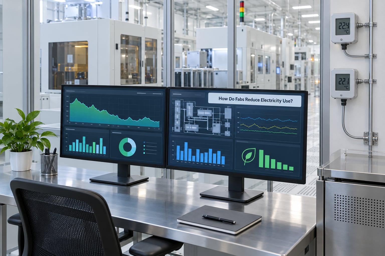
The levers are well known and none of them are dramatic on their own. Fabs have been running the same playbook for a decade, which is why efficiency gains show up as a few percent a year rather than an order of magnitude.
Efficiency at the HVAC and air handling level
Higher-efficiency fan motors, better filter selection, and variable-volume fan filter units that reduce airflow when a bay is idle all cut the largest fixed load. The limit is contamination control: air cannot be reduced below what the process specification requires, so this is a bounded optimisation rather than an open-ended one.
Tool-level power management
Sleep modes between lots, standby power states on idle chambers and scheduling software that sequences high-power tools off peak tariff windows are the most visible programmes. Tool-level work has a hard ceiling because tool suppliers own most of the standby behaviour.
Heat recovery
Chiller heat and cleanroom exhaust heat can be recovered for process preheating, utility water or facility heating. It works well in temperate climates and poorly where there is no useful thermal sink.
Leak detection and compressed air
Ultrasonic leak detection on compressed air and vacuum lines pays back quickly because leaks on a system that runs continuously become very expensive over a year. This is the cheapest item on the list and usually the fastest.
Process and yield optimisation
Removing a process step saves more than any facilities project. So does a yield gain, because every scrapped wafer carried the full energy cost of every step before it failed.
Powering strategy
Longer UPS ride-through, on-site generation sized to carry critical subfab loads, and demand-response agreements with the utility all manage the bill and the risk rather than the consumption. Memory fabs have led on this, because their load can be shifted across cycles more easily than a logic line’s.
One measured result worth noting: TSMC reported reducing peak power consumption of its EUV tools by 44%, saving roughly 190 million kWh and delivering about an 8% overall reduction in fab power. That is the shape of a realistic improvement, and it came from process and tool engineering, not from replacing a chiller.
Frequently Asked Questions
Do semiconductor fabs use a lot of water?
Yes. A large 300mm fab typically consumes millions of gallons of ultrapure water and process water each day, and much of it is recirculated rather than discharged. Water demand is driven by wafer cleaning steps, which rise sharply with process complexity and with each added patterning layer. Fabs also pull large volumes for cooling and for humidification control in the cleanroom, so water and electricity are sized together in almost every new facility.
Are semiconductor factories bad for the environment?
It depends on how the electricity is generated and how much material the process consumes. Semiconductor manufacturing emits more than 15 million metric tons of CO2 annually and accounts for over 30% of global perfluorocarbon emissions, largely from etch and deposition chemistry. Electricity carbon content varies enormously by region, so a fab’s Scope 2 emissions can differ by a factor of several between locations with the same process.
How much electricity does an aluminum smelter use?
An aluminium smelter potline typically operates in the hundreds of megawatts, and large smelter campuses run well into the gigawatt range. That puts a single smelter site in the same band as, or above, an entire leading-edge semiconductor fab, which typically draws 100 to 200 MW. Both industries share the same constraint: continuous, uninterruptible, very high load factor on a grid that must reserve firm capacity for them.
How much of a country’s electricity does TSMC use?
TSMC accounts for roughly 7 to 9% of Taiwan’s total electricity consumption, a share high enough to make every new fab approval a national energy discussion. The company reported about 16 TWh of consumption in 2022. By comparison, Samsung Electronics used roughly 19.3 TWh in 2021, and Intel consumed more than 10 TWh in 2022.
Who is TSMC’s biggest rival?
On electricity consumption specifically, Samsung Electronics is larger, using about 19.3 TWh in 2021 against TSMC’s roughly 16 TWh in 2022. In foundry market share, the picture is different: TSMC leads in both market share and revenue, and no single competitor is close. Intel, Samsung and the Chinese fabs are all competing aggressively for leading-edge capacity, which is the main reason sector energy demand is growing at about 7% annually.
How much energy will AI really consume?
AI’s electricity footprint is mostly upstream. Training and inference clusters draw tens of megawatts each, but they need leading-edge accelerators, and producing those is where the energy goes: a fab draws 100 to 200 MW continuously, and large AI dies carry around 1 to 2 kWh of manufacturing energy each. Rising AI demand is a primary reason fab power requests, grid interconnects and utility capacity plans are all under pressure.
Conclusion
A semiconductor fab consumes enormous electricity: roughly 100 to 200 megawatts of continuous load for a large 300mm site, about 1 TWh a year, with individual tools such as an ASML EUV scanner drawing around 1 MW each. But the total on its own tells you very little, because the same facility produces a wildly different energy intensity at 60% utilisation than at 90%.
So if you are evaluating any fab, benchmark three things separately: contracted and peak capacity in MW, annual consumption in TWh, and energy intensity in kWh per wafer or per good die. Any one of those on its own invites the wrong conclusion. As of 2026, that unit discipline is the fastest way to tell a solid efficiency claim from a marketing one.