A thermal interface material is a thermally conductive compound, film, gel or metal placed between a heat-generating chip and its heat spreader, lid, heat sink or cold plate, filling the microscopic air gaps between those surfaces so heat flows with far less resistance than through air.
Every watt a package dissipates becomes heat, and that heat has to cross several interfaces before it reaches a sink. A thermal interface material is the layer that makes each crossing efficient. Pick the wrong one, or apply it badly, and you trade a few degrees of junction temperature for throttling, accelerated ageing and a shorter product life.
Table of Contents
- What Are Thermal Interface Materials in Chip Packaging?
- How Thermal Interface Materials in Chip Packaging Work
- Why Are Thermal Interface Materials Needed?
- Which Types of Thermal Interface Materials Are Used?
- What do TIM1, TIM2 and TIM1.5 mean?
- Which TIM Has the Highest Thermal Conductivity?
- How Do Engineers Choose the Right TIM for a Package?
- How the choice changes for AI and HPC packages
- How Is a TIM Applied in Chip Packaging?
- Dispensing
- Screen and stencil printing
- Transfer printing and liner stamping
- Compression bonding and cure in place
- What Thermal Metrics Should Engineers Compare?
- What Causes Thermal Interface Materials to Fail?
- Pump-out
- Dry-out and oil migration
- Voids and trapped air
- Over-thick or nonuniform application
- Incomplete cure, outgassing and delamination
- Corrosion and chemical attack
- How Are TIMs Tested and Qualified?
- Frequently Asked Questions
- Is thermal paste better than a thermal pad?
- Do thermal interface materials need to be electrically conductive?
- What is the best bond line thickness for a chip package TIM?
- Can a damaged thermal interface layer be replaced?
- How long should chip packaging TIM last before it needs replacement?
- Should one TIM be selected for the package’s entire temperature range?
- Conclusion
What Are Thermal Interface Materials in Chip Packaging?
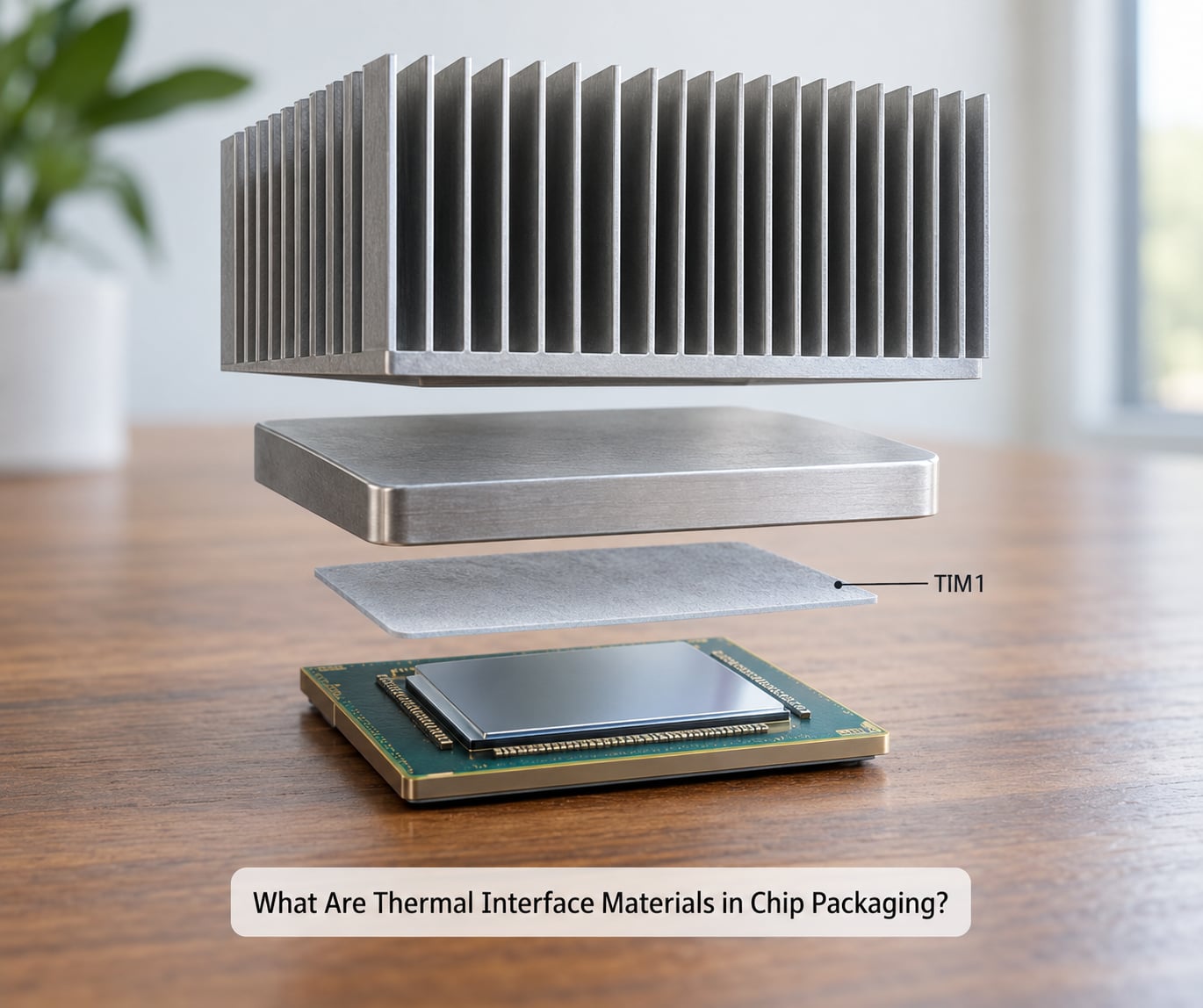
A TIM does four jobs, and the good ones do all four at once. It fills gaps, it wets both surfaces, it survives the temperature swings the package sees, and it holds a controlled thickness under whatever clamping force the assembly applies.
It is worth separating a TIM from the other materials that also sit between dies and substrates, because they solve different problems. None of them substitutes for a TIM.
| Material | What it does | Is it a TIM? |
|---|---|---|
| Solder (solder paste, solder ball) | Makes a mechanical and electrical interconnect, conducts some heat | No. Electrical plus structural, not a gap filler |
| Underfill | Glues flip-chip bumps and protects them from moisture and stress | No. Mechanical reinforcement, usually low conductivity |
| Die attach | Bonds the die to substrate or lid so it survives handling and reflow | Only when the attach chemistry is a soft thermally conductive TIM, which is exactly the TIM1 use case |
| Adhesive film or tape | Mechanically secures a lid or heat spreader | Sometimes. Thermally conductive adhesives are a TIM family |
| Thermal grease, pad, gel, PCM, metal TIM | Replaces air at a heat-transfer interface with something that conducts far better | Yes |
How Thermal Interface Materials in Chip Packaging Work
Two machined, lapped surfaces that look dead flat are not. Measured in nanometres, they are a field of peaks and valleys. Press them together and they touch at a small fraction of the apparent area. The rest of the interface is filled with air, which conducts roughly 0.026 W/m·K.
A liquid or soft TIM flows under pressure into those valleys and displaces the air. Replace air with a grease at 3 to 6 W/m·K and the real contact area no longer matters much, because almost all of the interface is now solid, conductive material. That single change is where the thermal performance comes from, not from a magic additive.
Performance at the interface is roughly the sum of three terms: the conduction through the TIM itself, which scales with thickness and falls as conductivity rises, and the contact resistance at each of the two surfaces, which depends on how well the TIM wets them.
That is why bulk conductivity alone is a poor predictor. A 8 W/m·K grease at 100 micrometres of bond line thickness (BLT) can lose to a 3 W/m·K pad at 25 micrometres with better wetting and lower contact resistance. The number in the datasheet describes a material, not your stack.
Why Are Thermal Interface Materials Needed?
Power density, not total power, is what makes the interface problem hard. A die-level power density measured in watts per square centimetre has climbed for two decades in AI accelerators, and stacked packages bury heat sources behind other silicon that cannot fan away.
Without a TIM the air voids in the interface dominate the thermal budget. Junction temperature climbs, and every consequence that follows is a package problem rather than a transistor problem.
Key effects worth watching for:
- Frequency throttling and clock derating once the part crosses its thermal limit
- Accelerated electromigration in on-die and package interconnects
- Delamination at die attach and lid attach as mismatched materials cycle
- Reduced product life, expressed in the package reliability models as a shortened time to failure
- Hot spots that never reach the bulk average, especially in 3D stacks
The same reasoning applies well outside processors. Power modules in silicon carbide and gallium nitride packages, memory stacks, LED dies, RF and photonics modules, and automotive electronics all cross the same kind of air-filled interface, just at different temperatures and with different mechanical constraints.
Which Types of Thermal Interface Materials Are Used?
Families differ less by conductivity than by mechanism. Some conduct by flow, some by phase change, some by being a solid metal, and some by combining softness with metal filler. The mechanism is what predicts reliability, thickness tolerance and how the material behaves under pressure.
| Family | Mechanism | Typical conductivity (W/m·K) | Electrical behaviour | Rework | Typical use |
|---|---|---|---|---|---|
| Grease and paste | Flows into surface voids | 1 to 6 | Usually insulating | Easy | General die-to-lid, board level, maintenance |
| Silicone oil or grease compound | Oil carrier with filler, slight bleed over time | 2 to 6 | Insulating | Easy | Consumer processors, test coupons |
| Phase change material (PCM) | Softens at a set temperature and fills the interface | 2 to 8 | Insulating | Moderate | Die-to-lid in flip-chip and BGA, power modules |
| Pad or film | Pre-formed solid or gel sheet, holds its shape | 1 to 9 | Insulating unless filled | Easy to peel | Memory stacks, low stress interfaces, module assembly |
| Putty and soft gel | Very soft, high conformability, absorbs stress | 1 to 6 | Insulating | Easy | Power modules, large irregular gaps |
| Adhesive film and tape | Bonding plus conduction, holds the lid mechanically | 1 to 8 | Can be designed either way | Poor | Lid attach, permanent assembly |
| Indium foil or soft metal | Conducts as a solid, conforms under pressure | around 20 to 80 depending on alloy | Conductive | Difficult | FCBGA lid attach, high-reliability servers |
| Sintered silver | Solid metal with a sintered bond, no polymer | high, well above polymers | Conductive | Very poor | Die attach and lid attach in high power and automotive |
| Liquid metal (gallium based) | Flows as a liquid, excellent conformance and stability | well above conventional greases | Conductive, and corrosive to aluminium | Messy, not clean-room | High power GPU and accelerator modules, experimental stack TIM |
| Graphene and nanomaterial composites | High conductivity filler in a thin film or sheet | Varies widely by grade and loading | Conductive | Varies | Thin bond lines, research and early production |
| Silver-filled gel | Soft gel carrying metal filler for conductivity plus conformance | Above unfilled gels | Conductive | Easy | Gap filling where a liquid metal is too aggressive |
What do TIM1, TIM2 and TIM1.5 mean?
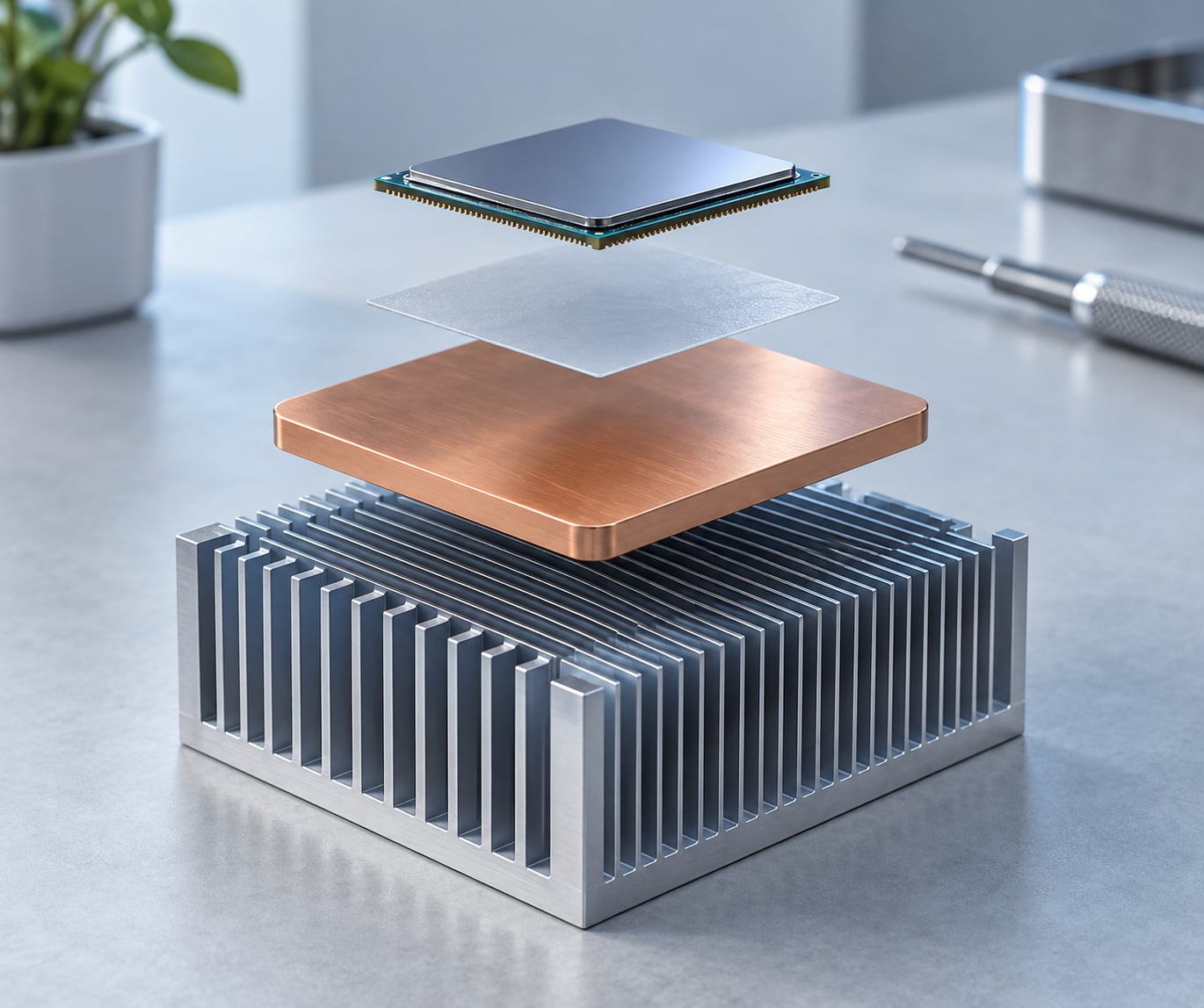
These are position labels, not chemistry labels. TIM1 is the interface between the die or lid and the package heat spreader, inside the package. TIM2 is the interface between the finished package and the external sink, cold plate or chassis, outside the package.
TIM1.5 is the newer single-layer approach: one TIM handles the whole path from die to cold plate, so one interface disappears. Fewer interfaces means fewer thermal resistances stacked in series, but it also means the single layer has to survive whatever warpage the package presents, and it puts a premium material inside the package bill of materials.
| Label | Position | Typical materials | Benefit | Trade-off |
|---|---|---|---|---|
| TIM1 | Die or lid to package heat spreader | PCM, gel, indium foil, liquid metal | Handles the die-level hotspot directly | Fine thickness control needed, affected by die-level warpage |
| TIM2 | Package to external sink or cold plate | Grease, pad, PCM | Large area, easy to apply and to rework | Large area means a big opportunity for voids and for heat to spread in a bad way |
| TIM1.5 | One layer, die to cold plate | Metal foil, high conductivity gel, liquid metal, graphene composite | Removes one interface and its contact resistance | Single point of failure, harder qualification, higher unit cost |
Which TIM Has the Highest Thermal Conductivity?
Among packaging materials, solid metals win outright. Indium-based soft metals, sintered silver and gallium-based liquid metal all conduct far better than any polymer family, and graphene composites reach high bulk numbers as fillers.
Among polymers and greases the ordering is narrower: conventional greases sit at the low end, phase change materials and filled pads in the middle, and highly filled composite films reach the top of the polymer range. Published ranges vary by grade, filler loading and test standard, so treat any single datasheet figure as a starting point for comparison, not a finished-stack result.
In practice the interface often matters more than the material. Four things dominate:
- Bond line thickness, which drives the conduction term directly
- Contact resistance at each surface, driven by wetting and surface preparation
- Void fraction, where a small number of large voids hurts more than a uniform sprinkle of small ones
- Clamping pressure and whether it is uniform across the lid
That is the honest answer to which TIM is best. The best material in the world will lose to a modest material applied thinly, cleanly and under even pressure.
How Do Engineers Choose the Right TIM for a Package?
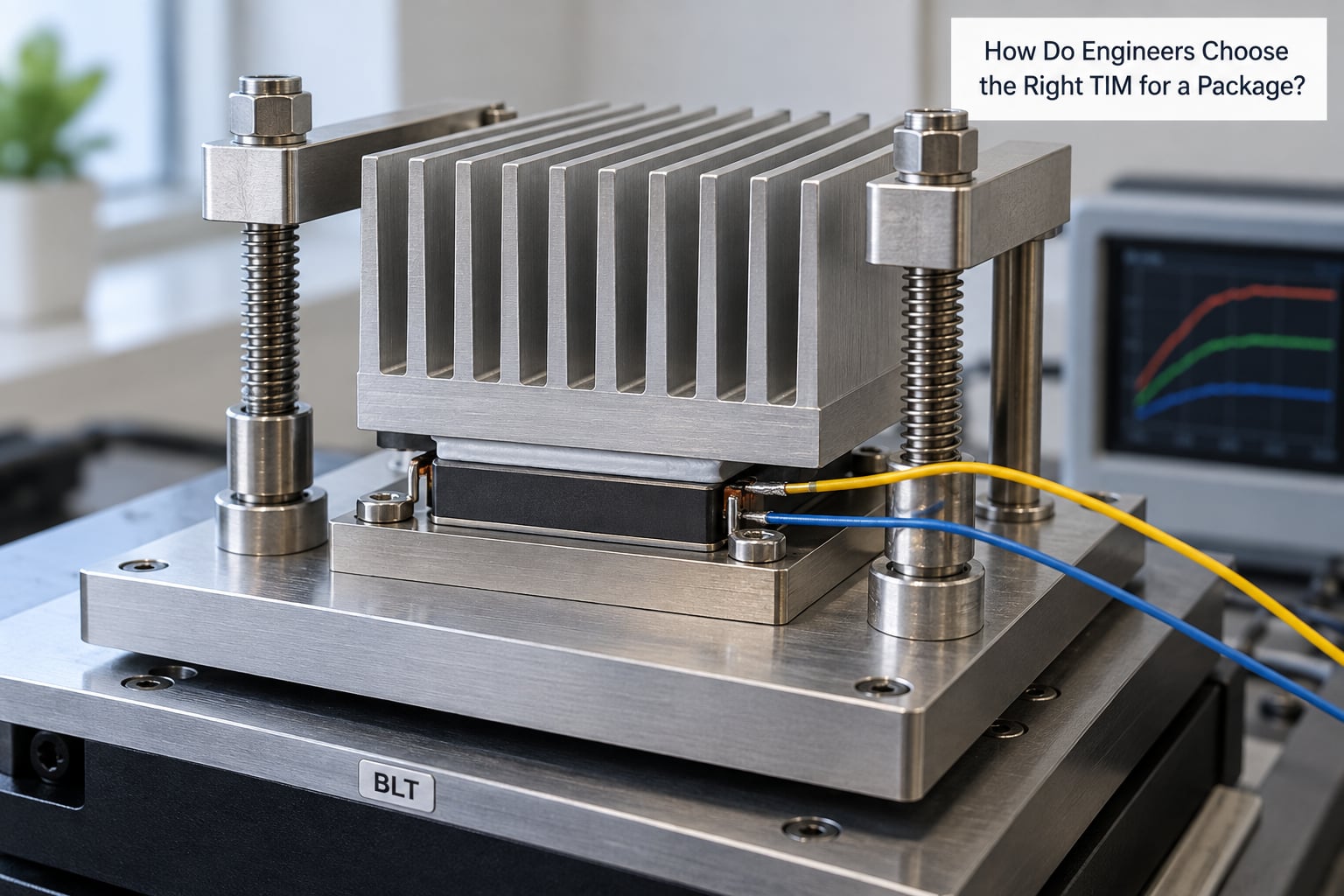
Selection starts from the package, not from the material data sheet. Work through these in order and most of the choice resolves itself before you compare candidates.
- Define the interface. Die to lid, lid to sink, package to cold plate, or die to cold plate in a single layer. The position decides which family is even viable.
- Set the thermal budget. How many degrees can this interface afford to add? Build the budget from the junction limit downwards and the TIM gets whatever is left after die, spreader and sink are accounted for.
- Set the target bond line thickness. A pre-formed pad implies a thickness, a dispensed grease does not, and a metal foil implies a very thin controlled layer. The process has to hold that target.
- Check the temperature range. The material has to stay soft or stable from the cold start to the worst-case junction, not just at room temperature.
- Decide the electrical requirement. Insulation, conductivity, or a defined withstand voltage between die and lid. A conductive TIM next to a bare die is a design decision, not a default.
- Check mechanical and chemical compatibility. Coefficient of thermal expansion mismatch, outgassing into a sealed cavity, corrosion of aluminium, and compatibility with the flux and cleaning chemistry used before assembly.
- Decide the assembly process. If the line cannot dispense, print or stamp the chosen material evenly at volume, a better material on paper is the wrong answer.
- Decide rework. Field-replaceable means grease, pad or gel. Not field-replaceable means you qualify it carefully and you accept a scrap yield on failure.
How the choice changes for AI and HPC packages
For AI and HPC modules the constraint set tightens in a specific way. Die and lid areas grow, so warpage grows with them, and nonuniform clamping pressure across a large lid produces a nonuniform bond line. That nonuniform BLT is a first-order thermal problem, not a cosmetic one, because thin spots raise local contact resistance exactly where the power density is highest.
The second change is buried hotspots. In 2.5D and 3D stacks, heat originates in a layer that no external sink can reach, so a spreading material at the die interface does more work than at the package interface. Analysts covering this space have pointed at liquid metal, indium foil, graphene sheets and silver-filled gels as the directions being funded for exactly that reason.
How Is a TIM Applied in Chip Packaging?
Application method is part of the material choice, because it decides the achievable bond line thickness and the void risk.
Dispensing
A syringe pump lays a controlled volume, or a stencil-defined volume, of grease, gel or PCM. It handles complex patterns and changing die sizes, and the accuracy depends on the fluid itself: viscosity change with temperature is a real process variable, and a stiff filler-loaded material is harder to dispense consistently than a low-viscosity one.
Screen and stencil printing
Through a screen or metal stencil, which is fast and repeatable at volume and works well for flat films on large areas. The mesh and the paste rheology set the printed thickness, so the printed film is usually a candidate for the interface where a fixed thickness matters more than flow.
Transfer printing and liner stamping
A film or pad is picked from a liner and stamped into place. This gives excellent thickness control and low void risk, at the cost of a fixed footprint, so it suits repeating sites rather than a bespoke outline.
Compression bonding and cure in place
The TIM is applied unformed and compressed between the die and lid, so the material itself defines the final thickness. A material that cures in place gains adhesion and stability with the assembly, and the cure schedule then has to fit inside the rest of the package flow.
Whatever the method, the surrounding steps decide whether the result is good. Both mating surfaces get cleaned and dried and handled with gloves. Clamping pressure is controlled and, for a large lid, as uniform as the tooling can make it. After assembly, the bond line is inspected by cross-section, by X-ray for voids, or by a thermal imaging screen under a controlled heat input. Rework feasibility follows directly from the method: a dispensed or stamped layer can be cleaned and redone, a cured adhesive cannot.
What Thermal Metrics Should Engineers Compare?
Most disagreements about TIMs come from comparing numbers measured under different conditions. These are the metrics that actually matter, and what each one tells you.
| Metric | Unit | What it reveals |
|---|---|---|
| Bulk thermal conductivity | W/m·K | Material property of the TIM itself, independent of how you apply it. Useful for ranking, misleading as a prediction |
| Interfacial or contact resistance | K/W or m²K/W | The cost of the two surfaces meeting. Often the dominant term in a real joint |
| Bond line thickness (BLT) | micrometres or mils | The thickness actually achieved in assembly. A specification target with a tolerance, not a wish |
| Thermal resistance of the joint | K/W or °C/W | The measured contribution of the assembled interface, the most useful number for a design trade study |
| Junction-to-ambient, RthJA | °C/W | The whole system, TIM included, under stated conditions. Compare only against identical test setups |
| Junction temperature | °C | The number the silicon actually sees. The final verdict, and the only one the product cares about |
| Void fraction or void map | percent or area | How much of the interface is air. Correlates strongly with local temperature rise |
Test conditions belong in the same line as the number. A joint resistance quoted at one clamping pressure, one bond line thickness and one contact area will not transfer to a different assembly.
What Causes Thermal Interface Materials to Fail?
Failures are rarely exotic. They come from a small number of repeatable mechanisms, and each has a matching prevention step and a matching symptom in test.
Pump-out
Repeated thermal cycling squeezes grease out from between the die and lid, and the interface thins over hundreds of cycles until contact is lost. It is most likely with a thin bond line, a hard mating surface and a stiff mounting load. Symptoms are a steady rise in thermal resistance with cycle count. Prevention means a material rated for pumped-out use, or a gel or pad with a filler network that resists it.
Dry-out and oil migration
The carrier oil in a grease separates from the filler over time, leaving a hard, insulating residue. The joint can look intact and conduct worse than it did on day one. High temperature and long dwell accelerate it.
Voids and trapped air
Air left in the interface by poor dispensing, contamination, or a warped lid. One large void is worse than many small ones because it becomes a local hot spot exactly under the heat source. Prevention is clean surfaces, controlled volume, even pressure and, where it matters, X-ray inspection before the lid is committed.
Over-thick or nonuniform application
Too much material is a thermal resistance, not a safety margin. A thick, uneven layer is also a symptom of inadequate clamping or a flatness problem upstream, and no TIM fixes either one on its own.
Incomplete cure, outgassing and delamination
A cure-in-place material that has not fully set, or that releases volatile components into a sealed package, creates voids that appear after the fact. Delamination at the die or lid interface follows from the same combination of bad wetting, contamination and thermomechanical stress.
Corrosion and chemical attack
A gallium-based liquid metal will attack bare aluminium, and some chemistries are aggressive toward bond wire, underfill or corrosion-sensitive metallisation. Check the compatibility list before you commit.
Diagnosing a failure in practice means matching the symptom to the mechanism: a resistance that climbs with cycling points to pump-out or dry-out, while a resistance that is already high at assembly points to voids, thickness or a flatness problem upstream.
How Are TIMs Tested and Qualified?
Thermal performance is measured on an assembled, defined interface, not on loose material. The standard approach heats one side of a defined stack with a controlled heat source and measures the temperature response on the other, reporting the joint thermal resistance in K/W or °C/W with the test conditions stated alongside.
Reliability qualification then asks the same interface to fail in a controlled way. The usual set includes temperature cycling and power cycling to expose pump-out and fatigue, high-temperature storage and high-acceleration stress testing for moisture and chemical mechanisms, vibration and mechanical shock for the bond, and a bond line inspection by cross-section or imaging. Ageing steps are read as a resistance shift against the baseline, not just as a pass or fail on a visual check.
Whatever test list you build, the acceptance criteria and the exact method should follow the standard that already governs your package, your customer requirements or the relevant industry specification for that device class. A number copied from another programme without the matching test geometry means very little.
Frequently Asked Questions
Is thermal paste better than a thermal pad?
Neither is better in general. A grease flows and can reach a very thin bond line, so it usually wins where the gap is small and the surface is well clamped. A pad holds a fixed thickness, survives vibration and repeated handling without pumping out, and is easier to apply consistently, which often wins in modules and memory stacks. The right answer comes from the required bond line thickness, the surface topography and the reliability environment, not from the paste label.
Do thermal interface materials need to be electrically conductive?
Usually no, and insulation is the default. Under a lid, the TIM is an insulator that happens to conduct heat well. Where the die or lid is at a live potential and the metal TIM families are used, the choice is deliberate: a metal or liquid metal TIM may be electrically conductive and can also corrode exposed aluminium. Decide from the electrical isolation requirement of the specific assembly, and check the dielectric and withstand voltage data before selecting a filled or unfilled material.
What is the best bond line thickness for a chip package TIM?
There is no single number, because the target follows the material and the process. A pre-formed pad or foil implies a specific thickness, typically tens of micrometres, while a dispensed grease can be squeezed much thinner. Thinner is generally better for conduction, but only down to the point where the process can no longer fill the interface without voids. Set the target from the material you intend to use, then hold it with a stated tolerance through clamping and cure, and treat nonuniformity as the real failure risk rather than the average value.
Can a damaged thermal interface layer be replaced?
That depends entirely on how it was applied. Grease, pads, gels and stamped films can usually be cleaned off the mating surfaces and reapplied, which is why those families are used where field service matters. A cured-in-place adhesive, a sintered metal bond or a bonded lid cannot be replaced without destroying the assembly, and a metal TIM in a sealed module usually means replacing the whole module. If rework is a requirement, write it into the material decision early, because it rules out several of the highest-performing options.
How long should chip packaging TIM last before it needs replacement?
There is no service interval, because a properly specified TIM is designed to last as long as the assembly, and qualified materials are expected to outlive the product line. What ends the life is a mechanism rather than a calendar: pump-out or dry-out in a grease, binder ageing in a gel, corrosion in a liquid metal, or delamination from thermomechanical stress. A package is designed to run to a defined life, so the right question is whether the qualified life for that material and geometry meets the target, not when someone expects to reapply paste.
Should one TIM be selected for the package’s entire temperature range?
Often yes for the die interface, with a caveat. A material that softens at its phase change temperature and stays stable above the worst-case junction will usually serve the whole range, and that is why phase change materials are common at die-to-lid. Where the package has a wide range with large thermal expansion swing, or a buried hotspot far from the sink, a single layer can hide a large local temperature difference. Either qualify one material across the full range with the extremes in the test profile, or split the path and qualify each layer separately.
Conclusion
Thermal interface materials in chip packaging are chosen in a fixed order: define the interface and its position, set the thermal budget it has to fit, fix the target bond line thickness and the clamping that will hold it, then screen candidates on conductivity, stability, electrical behaviour, assembly process, rework and qualification cost.
Start with the interface, not with the material data sheet. Once you know which layer the TIM has to be, how thick it has to be and how the line will clamp it, the family usually picks itself.