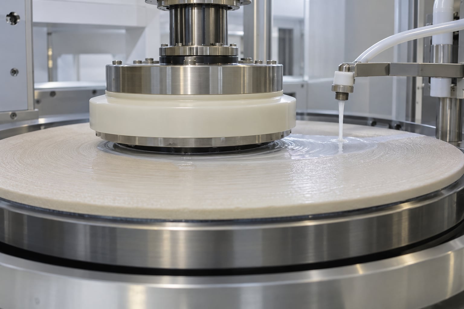
Chemical mechanical planarization, usually shortened to CMP, is the semiconductor process that flattens a wafer by pressing it against a rotating polishing pad while a chemically active slurry softens and abrades the surface. It is the reason a modern logic chip can carry more than twenty separate CMP steps and still be patterned. Updated October 2026.
If you have only ever heard the term, the short version is this: every layer a fab adds or removes leaves a bump or a dip, and those bumps accumulate until the lithography step cannot hold focus. CMP is the process that takes the topography away and hands the next layer a flat surface to work with.
What follows covers how the process works, what the equipment actually is, what the slurry is doing at the molecular level, how fabs control it, and how to diagnose a problem when the surface comes out wrong. It is written for process engineers, students, and design or packaging teams who need a working mental model rather than a recipe book.
Table of Contents
- What Is Chemical Mechanical Planarization?
- What planarization means on a fab floor
- Local versus global planarization
- How CMP differs from etching and grinding
- How Does Chemical Mechanical Planarization Work?
- Why pressure and speed matter
- Why temperature matters
- Why slurry flow matters
- What Are the Main Components of a CMP Process?
- How slurry actually reaches the pad
- How Does Chemical Mechanical Planarization Remove Material?
- How chemical mechanical planarization removes material one layer at a time
- Debris transport and why the pad matters
- Selectivity between materials
- Why Is CMP So Important in Semiconductor Manufacturing?
- Lithography depth of focus is the hard constraint
- What planarization buys the rest of the flow
- A realistic copper example
- CMP step counts climb with every node
- What Materials Are Planarized with CMP?
- What are CMP slurries made of?
- Common CMP slurry families
- The main material families and their specific headaches
- How Is CMP Controlled in a Production Fab?
- The knobs and what each one actually does
- Endpoint detection
- Measuring the result
- The coupled system problem
- What Defects and Failure Modes Can Occur?
- Symptom, likely cause, and the lever to pull
- Why CMP gets called a dirty process
- How Does CMP Differ from Etching, Grinding, and Electrochemical Machining?
- Where each one wins
- Frequently Asked Questions
- What is chemical mechanical planarization used for in semiconductor manufacturing?
- Is CMP the same as chemical etching?
- How do semiconductor manufacturers measure wafer flatness after CMP?
- What causes dishing and erosion during copper CMP?
- Can CMP be used at advanced process nodes such as 7 nm and 5 nm?
- What is the role of slurry in a CMP process?
- Conclusion
What Is Chemical Mechanical Planarization?
Chemical mechanical planarization is the semiconductor manufacturing process that removes material from a silicon wafer by combining the chemical reaction of a slurry with the mechanical abrasion of a rotating polishing pad, producing a surface that is flat and uniform across the full wafer diameter. Neither the chemistry nor the mechanics works well alone, which is where the name comes from and why the process is hard to control.
What planarization means on a fab floor
Planarization just means turning a surface with three-dimensional relief into one that is flat to a stated tolerance. It shows up everywhere in the flow: shallow trench isolation, inter-level dielectric, tungsten plugs, copper damascene, replacement metal gate, through-silicon via reveal. Each of those steps adds height somewhere on the wafer, and each of them needs the leftover height taken back out before the next one starts.
The tolerance is tighter than most people assume. Across a 300 mm wafer, the difference between the highest and lowest point of the finished surface is measured in tens of nanometres, and that number is what every downstream process budget is built on.
Local versus global planarization
This is the single most useful distinction in the whole field, and it explains which CMP steps are easy and which ones are hard.
Local planarization means the surface immediately around each feature is flattened, but the overall height of the wafer may still slope or undulate. Spin-on glass does this, and so does any CMP step where the remaining topography is small compared with the feature pitch.
Global planarization means the whole wafer surface ends up on one flat plane, regardless of how far above or below it the pattern originally sat. That is what CMP does that almost nothing else can, because a soft pad conforms to the surface and self-levels.
Everything from shallow trench isolation fill onward depends on global behaviour. CMP is one of the few steps in the entire flow that flattens across the entire 300 mm, which is also why it is where most of the yield loss lives.
How CMP differs from etching and grinding
Wet etching removes material chemically and is fast but it rounds corners and cannot easily make a surface flat, because it has no mechanical reference plane. Grinding removes material mechanically and is flat but leaves subsurface damage and a strained layer. CMP sits between the two: the pad supplies a flat reference plane and the chemistry supplies the selectivity and damage control that a grinder lacks.
That combination is what lets a fab stop at a precisely defined film thickness instead of a vaguely defined time. The table near the end of this article sets CMP against etching, grinding and electrochemical machining side by side, with the practical limits of each.
How Does Chemical Mechanical Planarization Work?
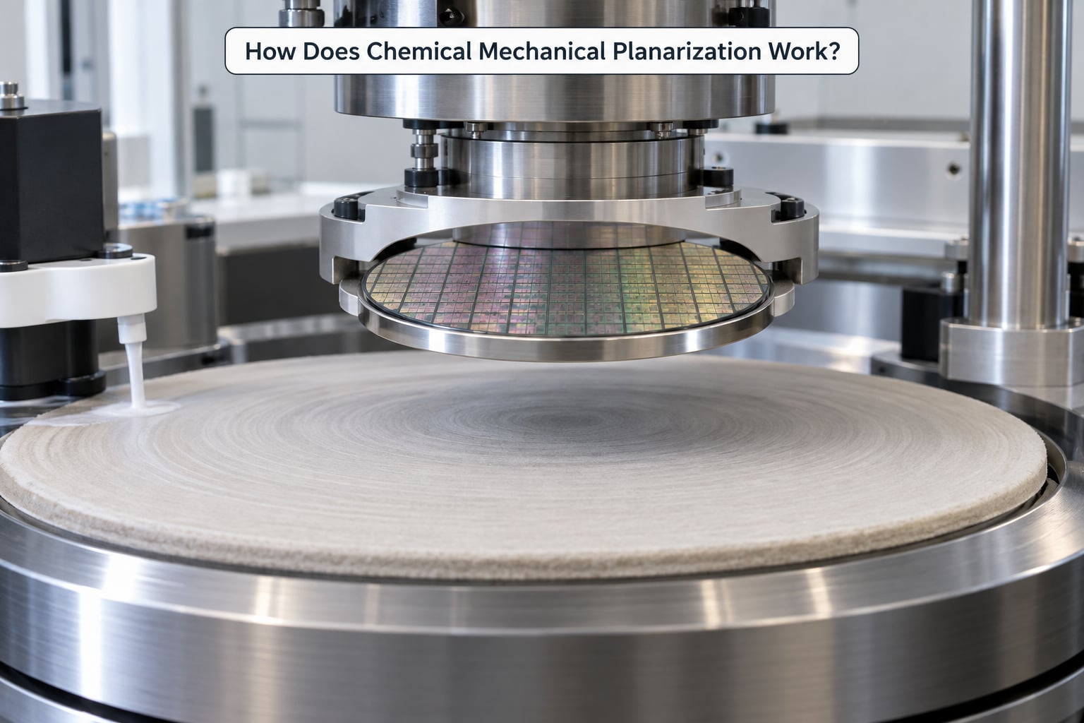
CMP works because a soft pad pushes harder against whatever stands highest. A raised feature contacts the pad more aggressively, gets abraded faster, and moves down toward the surrounding surface. That feedback loop runs until the whole face sits on one plane. The chemistry decides what counts as removable; the mechanics decide how fast it leaves.
The whole flow, in order:
- Prepare the wafer. Load the wafer into a carrier head and wet the surface so the film being polished stays chemically active.
- Condition the pad. Run a diamond conditioning disk against the polishing pad to refresh the surface asperities before the wafer arrives.
- Deliver slurry. Dispense the formulated slurry between the wafer and the pad at a controlled flow rate and concentration.
- Apply down-force and speed. Press the wafer into the pad with a controlled load and start relative motion between carrier and platen.
- Polish the film. The chemistry softens or oxidizes the surface into a thin layer that the abrasive can remove, and raised areas remove faster.
- Detect the endpoint. A sensor watches the surface and calls the step when the remaining film hits the target thickness.
- Clean and inspect. Rinse and dry the wafer, then measure thickness and uniformity before it goes back to the process.
Every one of those seven steps can end a step early or late, which is why CMP problems rarely point at a single cause.
Why pressure and speed matter
The standard model for removal is Preston’s equation: material removal rate equals a process constant times pressure times velocity. Pressure comes from the carrier head down-force spread across the wafer face. Velocity comes from the combination of platen rotation, carrier rotation, and how much the carrier sweeps across the wafer.
Because the equation is multiplicative, changing one knob changes the whole picture. Raise pressure and you remove faster but you also remove faster where the surface is already exposed, which shows up as erosion. Raise velocity and you get more heat and more slurry splash. Neither knob moves removal rate alone.
Why temperature matters
Friction between the pad, the slurry and the wafer generates real heat, and the chemistry is temperature sensitive. As the pad warms through a batch, reaction rates climb and removal drifts upward unless the platen is cooled. This is one of the reasons a step that ran at the start of a batch does not run the same way at the end.
Why slurry flow matters
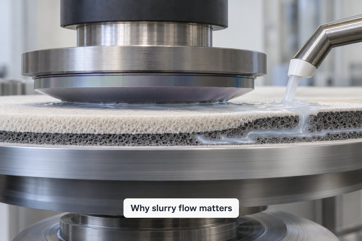
Flow sets how fast fresh chemistry arrives and how fast debris leaves. Too little flow and the slurry under the wafer goes stale: reaction products build up, removal slows, and the surface can roughen. Too much flow and the pad lifts off the wafer, a condition often called hydroplaning, which shows up as a sudden collapse in removal rate with no change in any other parameter.
A fresh supply of abrasive under the wafer is what keeps the contact chemistry steady, so flow is really a chemistry knob disguised as a plumbing knob.
What Are the Main Components of a CMP Process?
A CMP tool is a platen, a pad, a carrier head, a slurry delivery subsystem, a pad conditioner, some form of endpoint sensing, and a wet clean station downstream. Each component has a job and each has its own failure modes, and the interactions between them are where most of the process engineering lives.
| Component | Function | Typical process concern |
|---|---|---|
| Polishing head (carrier head) | Holds the wafer face-down and applies controlled load, often with several independently pressurised zones | Down-force profile, edge pressure, wafer slip, temperature drift across the face |
| Platen | Rotating table that carries the polishing pad and provides the reference plane | Rotation speed, runout, flatness, platen temperature over a batch |
| Polishing pad | Soft porous layer that conforms to the wafer and supplies the abrasive contact | Glazing, uneven wear, hardness drift, cut rate loss if conditioning is too light |
| Slurry delivery system | Stores, mixes, dilutes, filters and dispenses slurry to the pad | Flow drift, clogging, concentration drift, cross-contamination on multi-slurry tools |
| Pad conditioning system | Presses a diamond disk against the pad to rebuild surface asperities | Conditioning force and frequency, pad wear rate, debris generation |
| Endpoint detection | Signals when the remaining film reaches target thickness | Choosing optical, motor current or eddy current sensing; over-polish and under-polish |
| Post-CMP clean | Removes slurry particles, ions and metal residues before the next step | Particle counts, brush conditioning, drying marks, cleaning selectivity to the film |
How slurry actually reaches the pad
Worth spelling out, because it is the subsystem people forget. Slurry usually arrives at the tool in one of two ways: as a discrete batch pumped through a pipe to a dispense arm above the pad, or continuously with a recirculating loop. Either way it passes through in-line filtration on its way to the pad.
A recirculating loop has a filter, and that filter clogs. As it clogs, the pressure drop across it rises, the flow falls, and removal rate drops with it. The wafer does not scratch and nothing alarms. The engineer sees a slow step that looks like a slurry chemistry problem and spends a day chasing the wrong thing.
Point-of-use dilution is the common fix: water is blended in at the pad rather than at the tank, so the delivered concentration stays on target even as the supply tank ages. Slurry also dries and hardens in idle lines, which is why flush-and-purge after idle periods is standard practice and not optional.
How Does Chemical Mechanical Planarization Remove Material?
Material comes off the wafer because the slurry holds it in suspension and the pad supplies the force. Rough pad asperities press the surface, abrasive particles scratch and gouge it, and the chemistry continuously re-softens the exposed surface so fresh material keeps being attacked instead of forming a passivated layer that polishing would stall against.
How chemical mechanical planarization removes material one layer at a time
The sequence at a single point on the surface looks roughly like this. A pad asperity presses down. An abrasive particle trapped between the asperity and the film shears off a chip of material. Chemicals react with the freshly exposed surface and make the next layer softer. The chip is carried away in the slurry, opening space for the next particle.
Two rate processes compete the whole time: mechanical removal, which is roughly proportional to pressure and velocity, and chemical reaction, which depends on the slurry and the temperature. Balance them and you get smooth, fast removal. Let either one dominate and the surface shows it.
Let the chemical reaction dominate and you get chemical etching behaviour, with rounded features, undercut and poor selectivity. Let mechanical removal dominate and you get a scratchy surface with subsurface damage and poor feature control. The entire art of CMP is keeping those two in balance, and that is why pad hardness, slurry chemistry and pressure are tuned together rather than one at a time.
Debris transport and why the pad matters
The pad is not a flat sheet. It is a porous structure with a soft top surface and a harder backing layer, and the pore structure is what moves debris away from the contact zone. When pores clog or the surface glazes over, debris stays in the contact zone and starts cutting instead of clearing. Removal rate falls and scratching rises, and both problems trace back to the same change in pad condition.
Selectivity between materials
Selectivity is the ratio of removal rates for two films in the same slurry. Copper CMP relies on a protective film forming on the copper so the surrounding dielectric polishes faster and copper dishes only slightly. Low-k dielectrics are porous and mechanically weak, so the challenge runs the other way: polishing the overburden hard without damaging a film that has little mechanical strength to begin with.
Whenever a CMP step names both a film and a stop layer, selectivity between them is the number that decides whether the step works.
Why Is CMP So Important in Semiconductor Manufacturing?
CMP matters because step heights accumulate. Every layer patterned adds relief, every layer deposited fills some of it and creates new relief, and none of these operations is perfectly flat to begin with. Left alone, the topography grows until the process breaks.
Lithography depth of focus is the hard constraint
193 nm immersion lithography has a depth-of-focus window on the order of plus or minus 50 nm. That means a wafer with 200 nm of step height cannot be patterned in a single exposure no matter how good the scanner is. The field simply cannot be in focus across the surface.
EUV narrows the window further. Each successive node shrinks the tolerance and pushes more work onto planarization.
What planarization buys the rest of the flow
- Flat surfaces for lithography. Focus and overlay hold across the full wafer instead of only over flat regions.
- Uniform deposition and etch. Most deposition and etch processes are not line-of-sight, and a patterned surface gives them a thickness to compensate for. Remove the pattern and the process simplifies.
- Reliable via and contact fill. A tungsten plug or copper fill lands on a flat floor rather than a slope, which keeps contact resistance predictable.
- Continuous barrier and seed layers. Barrier metal has to be a continuous film. Over topography it breaks at high points, and CMP is what makes it continuous.
- Multilayer interconnects. Fifteen or more metal layers are only manufacturable if each one starts flat.
A realistic copper example
Consider a copper damascene step. Trenches and vias are patterned into a low-k dielectric, copper is deposited, and it sits proud of the dielectric everywhere. A copper CMP step removes the overburden until only the copper inside the features remains.
Because copper is softer and reacts faster than the surrounding dielectric, the polishing has to be controlled on two fronts at once. Press too hard and the copper inside the wide lines removes faster than the overburden does, leaving a dished profile. That dish is exactly what breaks continuity in the layer above it. The step is a balance between removing everything above the dielectric and removing nothing below it.
CMP step counts climb with every node
As the process scales, CMP steps are added rather than removed. Broadly, planarization counts were modest through the mature planar era and then climbed sharply once copper damascene, then multi-gate transistors, then nanosheet structures entered the flow. A leading-edge logic node in 2026 requires more than twenty-five distinct CMP steps, and each one carries its own metrology, its own slurry and its own defect sensitivity.
What Materials Are Planarized with CMP?
Nearly everything a fab builds with. The material being polished sets the abrasive, the pH, the selectivity requirement and the defect mode that shows up when something goes wrong.
What are CMP slurries made of?
A CMP slurry is a formulated water-based suspension with four functional parts. Abrasive particles do the physical cutting, and the common choices are colloidal silica, fumed ceria and fumed alumina. An oxidizer such as hydrogen peroxide drives the surface reaction, and its strength sets how fast the chemistry works. An inhibitor or chelator controls which film reacts, with benzotriazole the classic copper example and glycine or ammonium citrate common in dielectric slurries. Surfactants and pH buffers manage wetting, particle suspension and reaction rate.
Particle size matters as much as chemistry. Slurry that leaves large agglomerates behind is the single most common root cause of line defects and scratches.
Common CMP slurry families
| Slurry family | Primary abrasive | Typical pH | Target film | Key selectivity concern |
|---|---|---|---|---|
| Silica-based dielectric slurry | Colloidal silica | Alkaline | Oxide and low-k dielectric | Protecting the underlying stop layer and the low-k film itself |
| Ceria-based slurry | Fumed ceria | Near neutral to mildly acidic | Tungsten and other soft metals | Cutting fast while limiting scratching of the metal |
| Alumina-based slurry | Fumed alumina | Acidic | Aluminum and harder films | Residue removal against the stop layer |
| Copper slurry with inhibitor | Colloidal silica | Alkaline | Copper damascene overburden | Dishing in wide lines versus over-polish residue |
| Hard abrasive slurry | Alumina or ceria | Varies | Silicon carbide and hard substrates | Sub-surface damage and microcracking in brittle materials |
The main material families and their specific headaches
Copper is soft, ductile and chemically active, so it polishes fast and dishes easily. Inhibitor chemistry and low down-force are the main controls.
Aluminum polishes reasonably but leaves stubborn particles because it smears rather than cuts cleanly. Post-CMP clean chemistry has to fight that.
Tungsten sits in plugs and contacts and needs to clear without dishing, so ceria-based slurries are common. Scratching is the recurring complaint.
Dielectric films are the volume CMP application. Oxide is straightforward; low-k is not, because low-k materials are porous and mechanically weak and take damage from the pad itself, not only from the abrasive.
Silicon shows up in wafer thinning, TSV reveal and channel-hole pre-flattening in 3D NAND, where hundreds of vertical structures have to be flattened at once.
Silicon carbide and other wide bandgap materials are hard and chemically inert. They need aggressive abrasives and they chip and microcrack rather than scratch, and they polish far more slowly than silicon. GaN-on-SiC for radio frequency devices has the same problem in a different stack.
How Is CMP Controlled in a Production Fab?
Fabs control CMP by holding a small set of recipe variables at values that produce a target thickness with a target uniformity, and by measuring after every step so drift shows up on one wafer instead of a whole batch. Published recipes never describe the settings themselves, because they are process IP, but what each knob physically changes is well understood.
The knobs and what each one actually does
| Variable | What it changes physically | What goes wrong when you turn it the wrong way |
|---|---|---|
| Carrier head down-force | Contact pressure across the wafer face, and therefore how hard raised features press into the pad | Too high erodes the pattern; too low leaves residue and slows removal |
| Back-pressure profile across zones | Whether the wafer edge receives the same load as the centre | A flat profile gives edge dishing and a thickness ring across the wafer |
| Platen rotation speed | Relative velocity and the shear force on the pad surface | Too fast heats the platen and pushes removal rate up mid-batch |
| Carrier rotation speed | Averages contact pressure over the wafer face | Too slow gives uneven wear tracks and a spiral in the removal pattern |
| Carrier sweep | How the contact zone moves across the wafer, which is what evens out removal | Poor sweep leaves locally fast and slow bands |
| Slurry flow rate | How fast fresh chemistry arrives and debris is carried away | Too low causes stale chemistry; too high lifts the wafer off the pad |
| Slurry concentration at point of use | Number of active abrasive particles in the contact zone | Drift here looks exactly like a chemistry change and gets misdiagnosed |
| Pad condition and conditioning | Whether pad asperities are sharp enough to cut | A glazed pad removes slowly and scratches at the same time |
Endpoint detection
Endpoint detection is how the step knows when to stop, and it is where a lot of the yield lives. Three approaches are common, and they suit different situations.
Optical endpoint detection watches the interference colour of the wafer surface through the slurry film. As the film thins, the colour shifts, and the tool reads the shift to calculate remaining thickness. It works well on dielectric films and gives a direct thickness signal, but it needs a clear optical path and it struggles on strongly patterned or heavily coloured films.
Motor current endpoint detection watches the motor that drives the platen or the head. When the film thins, friction changes, the motor current changes, and that change marks the endpoint. It needs no optical access and works on any material, but the signal is indirect, so it usually needs calibration against a measured thickness.
Eddy current sensing measures the film thickness through a change in an induced magnetic field. It is fast and accurate on conductive films such as metal, and it does not apply to dielectrics.
Over-polish is worse than most people expect. A step that runs past its endpoint does not just remove too much metal, it removes into the barrier and liner and leaves a surface the next deposition cannot stick to. Under-polish is recoverable, over-polish usually is not.
Measuring the result
Three numbers describe a CMP result, and engineers read them constantly.
Thickness is the average remaining film. It is measured with spectroscopic ellipsometry for dielectrics and with eddy current probes or cross-sectional analysis for metal films.
Within-wafer non-uniformity measures how much the thickness varies across the wafer itself. This is the number that determines whether a step is manufacturable at all.
Total thickness variation measures the spread across the whole lot rather than inside one wafer, which captures wafer-to-wafer drift as well.
Surface roughness is reported as Ra or Rq and is measured with atomic force microscopy on a small sample, usually at the end of a qualification rather than on every wafer. An unusually low Ra on a soft film is often a warning sign of dishing rather than a good result.
The coupled system problem
Here is the practical point that catches new engineers. Slurry chemistry and pad condition are not independent. Pad wear changes the surface the chemistry acts on, so the same slurry removes at a different rate on a worn pad than on a fresh one. Conditioning restores the pad, which changes the rate again. That is why tuning slurry on a pad that is quietly glazing produces a result that does not transfer to the next lot.
The same coupling shows up across subsystems: flow rate affects pad temperature, pad temperature affects reaction rate, reaction rate affects pad wear. Practitioners describe this as the reason CMP is under-documented, and it is accurate. Almost everything in this process is connected to something else.
What Defects and Failure Modes Can Occur?
CMP defects fall into four broad groups: geometry defects where the profile is wrong, surface defects where the finish is wrong, particle defects where something foreign is on the wafer, and wafer-level damage from handling. The useful skill is going from symptom to cause to lever quickly, because the symptom usually appears on an inspection tool hours or days after the step that caused it.
Symptom, likely cause, and the lever to pull
| Symptom | Likely cause | Corrective lever |
|---|---|---|
| Dishing in wide lines or large open areas | Pattern density effect: soft or over-pressured copper removes faster where there is more of it | Reduce down-force, reduce pattern density in the layout, lower slurry pressure in high-density regions |
| Erosion, the opposite problem | High-pressure regions at pattern edges cut faster than the field | Lower carrier pressure and lengthen polish time to reach the same thickness |
| Scratches across the wafer | Slurry agglomerates, a glazed pad, pad debris, or a damaged conditioning disk | Improve filtration and point-of-use dilution, increase conditioning, check for pad debris and disk damage |
| Lines and streaks | Particle carryover from the slurry loop or from the post-CMP clean | Filter changes, flush the delivery loop, check brush conditioning and drying |
| Removal rate declining through a batch | Pad glazing, platen temperature rising, or a partially clogged filter reducing flow | Increase conditioning, check platen cooling, check filter pressure drop |
| Sudden collapse of removal rate with no parameter change | Pad lifting off the wafer because flow or pressure moved outside its working window | Bring flow and pressure back into range, check for air in the slurry line |
| Thickness ring or edge-first removal | Back-pressure profile not compensating for the edge of the wafer | Retune the multi-zone back-pressure profile |
| Residue after the clean step | Cleaning selectivity wrong for the film, or a chemical clean that etches the film slightly | Adjust the clean chemistry and brush loading, check drying conditions |
| Delamination or peeling of an overlying film | Contamination left by the clean step, or a film deposited on a surface with high roughness | Improve post-CMP cleaning, reduce roughness at the polish step |
| Chatter marks or repeating bands on the surface | Mechanical resonance between carrier, pad and platen at a particular speed | Move platen or carrier speed away from the resonance, check carrier bearing condition |
| Particles appearing in the middle of the field | Slurry dried in an idle line and re-dispersed when the tool restarted | Flush and purge after idle periods, tighten the idle schedule |
| Cross-contamination between two steps on the same tool | Shared slurry lines carrying residue from one chemistry into the next | Separate the delivery paths, validate the flush sequence between chemistries |
Why CMP gets called a dirty process
Because it is. Slurry residue, particulate and metal contamination are the reason CMP is treated differently from most other modules, and the post-CMP clean is not a convenience step, it is a required one. A fab that skips or shortens the clean will see yield fall at the next few steps rather than at the clean itself, which is what makes the diagnosis slow.
There is an environmental side too. Slurry contains metal oxides, oxidizers and amines, and waste handling at scale is a real operational cost that most general explainers skip.
How Does CMP Differ from Etching, Grinding, and Electrochemical Machining?
CMP is the only mainstream surface process that flattens across a whole 300 mm wafer while controlling the damage it leaves behind. Each alternative is better at something and worse at something else, and the fab uses whichever fits the layer it is building.
| Method | How it removes material | Final flatness | Selectivity | Main limitation |
|---|---|---|---|---|
| CMP | Chemical reaction plus mechanical abrasion with a soft pad | Global, across the whole wafer | Good, tunable through chemistry | Slow, consumable-heavy, generates particles |
| Wet or dry etching | Chemical or plasma reaction only | Poor, rounds corners and follows the pattern | Very good | Cannot produce a flat surface across topography |
| Mechanical grinding | Abrasion against a hard wheel | Flat within the machined area | Low | Subsurface damage, residual stress, edge chipping |
| Electrochemical machining | Anodic dissolution in an electrolyte | Very flat in cut areas | Good on conductive materials | Conductive materials only, requires fixturing and electrolyte control |
| Spin-on glass | Flow of a liquid dielectric during spin | Local planarization only | Not applicable | Cannot globally flatten, prone to thickness variation on topography |
| BPSG reflow | Thermal flow of a boron-doped glass | Local to moderate | Not applicable | High thermal budget, boron diffusion risk |
| Resist etch-back | Plasma etch of an overlying resist to flatten | Local | Limited by the underlying stack | Requires a removable sacrificial layer |
Where each one wins
Etching wins wherever the pattern itself defines the result and material selectivity matters, which is most pattern forming steps. Grinding wins for wafer thinning and back-grinding where bulk material has to come off fast and the damaged layer can be tolerated or removed later. Electrochemical machining wins for conductive materials needing very flat, damage-free surfaces in small areas.
CMP wins the one job none of the others can do: taking a wafer with real topography and returning the whole 300 mm face to one flat plane, with the profile control to keep the next layer intact.
Frequently Asked Questions
What is chemical mechanical planarization used for in semiconductor manufacturing?
CMP is used to flatten wafer surfaces between process steps so the next layer can be built on a predictable base. Typical uses include shallow trench isolation, inter-level dielectric, tungsten contact plugs, copper damascene, replacement metal gate and through-silicon via reveal. Without it, step heights accumulate and lithography cannot hold focus across the wafer.
Is CMP the same as chemical etching?
No. Chemical etching removes material through a reaction alone, which gives it excellent selectivity but leaves a surface that follows the pattern rather than flattening it. CMP combines that chemistry with mechanical abrasion against a soft pad, and the pad supplies a flat reference plane. The pad is what makes the result globally flat instead of merely shaped.
How do semiconductor manufacturers measure wafer flatness after CMP?
Engineers check three numbers after each step: remaining film thickness, within-wafer non-uniformity across the 300 mm face, and total thickness variation across the lot. Thickness comes from spectroscopic ellipsometry for dielectrics and eddy current probes for metals. Surface roughness is sampled with atomic force microscopy, usually at qualification rather than on every wafer.
What causes dishing and erosion during copper CMP?
Both come from pattern density. Copper is softer and reacts faster than the surrounding dielectric, so wide lines and open areas with more copper polish faster and sink below the field, which is dishing. Where high-pressure pattern edges cut harder than the flat field, material is removed faster there, which is erosion. The controls are lower down-force, a tuned back-pressure profile and layout pattern density.
Can CMP be used at advanced process nodes such as 7 nm and 5 nm?
Yes, and advanced nodes depend on it more, not less. Each smaller node adds CMP steps because tighter lithography depth of focus and more complex structures require more flattening. Leading-edge logic nodes in 2026 need more than twenty-five separate CMP steps. The tools are more precise and the metrology tighter, but the core mechanism is unchanged.
What is the role of slurry in a CMP process?
Slurry is the working fluid and it does three jobs at once. Abrasive particles such as colloidal silica, fumed ceria or fumed alumina cut the surface, chemicals such as hydrogen peroxide soften or oxidize it so it can be cut, and inhibitors or chelators protect the film that must survive. Surfactants and pH buffers keep particles suspended and reaction rates on target.
Conclusion
CMP is a controlled combination of chemistry, mechanical polishing, cleaning and metrology, and the whole thing behaves as one coupled system. Slurry chemistry, pad condition, flow, pressure and temperature all interact, which is why a single-symptom fix almost never holds for more than a lot or two.
If you are new to this, four things are worth understanding first. Start with the purpose: planarization exists because step heights break lithography focus. Then learn the equipment flow, from carrier head and pad through delivery, conditioning, endpoint detection and the clean step. Next, grasp that slurry and pad are tuned together and neither one means much on its own. Finally, understand the trade-off at the centre of every recipe: more removal rate means less flatness control, less selectivity and more defect risk, and every knob in the process moves along that same axis.
Once those four are in place, the rest is specific applications and specific defect modes, and both are far easier to learn.