In chemical vapor deposition vs physical vapor deposition, the deciding factor is where the material comes from. PVD moves atoms physically off a solid target by evaporation, sputtering or arc discharge, and CVD builds the film by reacting gaseous precursors on a heated substrate. Pick PVD for metals, adhesion layers and low-temperature work on precision parts; pick CVD for dense, conformal dielectrics and epitaxial films. The rest of this guide breaks down where each one wins and why.
Both are vapor-phase thin film deposition processes, and both are used in semiconductor manufacturing, optics, tooling and surface engineering. The difference is not academic. Mechanism determines step coverage, substrate temperature, how strongly the film bonds to the part, and what the film can be made of.
This comparison was updated for 2026, and the temperature, pressure and thickness ranges below reflect how these two process families actually behave in production lines today.
Table of Contents
- Chemical Vapor Deposition vs Physical Vapor Deposition at a Glance
- How Chemical Vapor Deposition Works
- How Physical Vapor Deposition Works
- Film Quality, Uniformity, and Step Coverage
- Materials and Film Properties
- Deposition Rate, Temperature, and Equipment Cost
- Chemical Vapor Deposition vs Physical Vapor Deposition: Which Is Better?
- Which Should You Choose?
- Frequently Asked Questions
- What is the main difference between CVD and PVD?
- Is CVD more conformal than PVD?
- Which method deposits metals and which deposits dielectrics?
- Does CVD or PVD provide better step coverage in trenches?
- Can physical vapor deposition be used for high-aspect-ratio structures?
- How do I choose between CVD and PVD for a semiconductor process?
- Conclusion
Chemical Vapor Deposition vs Physical Vapor Deposition at a Glance
| Criterion | Chemical Vapor Deposition (CVD) | Physical Vapor Deposition (PVD) |
|---|---|---|
| Mechanism | Chemical reaction of gaseous precursors at or near the substrate | Physical transfer of atoms from a solid target |
| Source material | Volatile precursor gas or liquid, delivered by mass flow controllers | Solid target of the material being deposited, or feedstock for evaporation |
| Chamber pressure | Atmospheric down to low pressure; PECVD sits in the middle | High vacuum, roughly 10^-2 to 10^-6 torr depending on process |
| Substrate temperature | Typically 500 to 1100 degrees C; tool-coating CVD often runs near 1000 degrees C | Typically 200 to 500 degrees C; many tool coaters stay under 540 degrees C |
| Typical film thickness | 1 to 50 micrometers in a single run | 0.1 to 5 micrometers in a single run |
| Step coverage | Conformal, with good coverage into trenches and vias | Line-of-sight, poor inside deep narrow features |
| Film density and purity | High density, low impurity when chemistry is clean | Very high purity, but more open and porous microstructure |
| Bond to substrate | Chemical or diffusion bond, resists galling and delamination | Mostly physical adhesion, can improve with a bond layer |
| Masking and selectivity | Difficult. Precursor gas reaches every exposed surface | Straightforward. Plugs and fixtures block the line of sight |
| Byproducts and safety | Halogenated or toxic byproducts, needs scrubbers and gas handling | Few chemical byproducts, but high-voltage and vacuum hazards remain |
| Typical uses | Dielectrics, epitaxial films, hard coatings, tungsten and nitride films | Metal interconnects, seed and barrier layers, hard and decorative coatings |
How Chemical Vapor Deposition Works
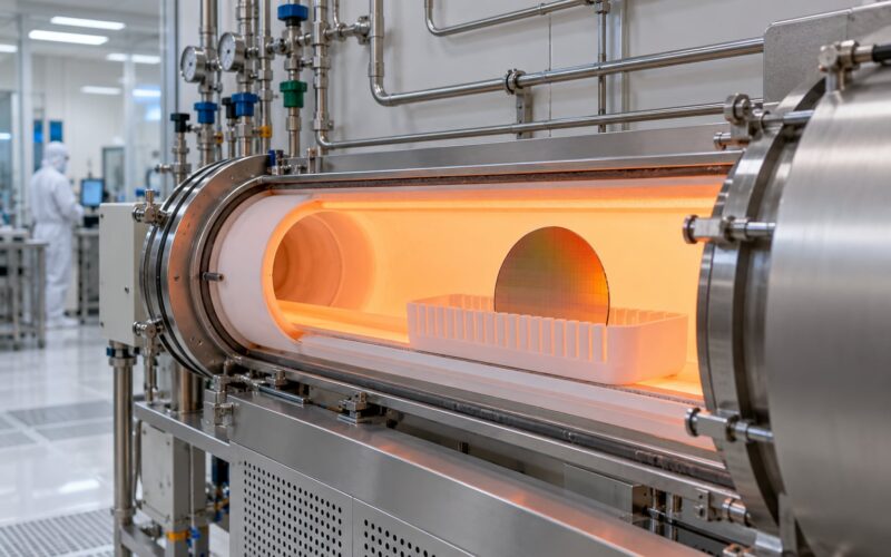
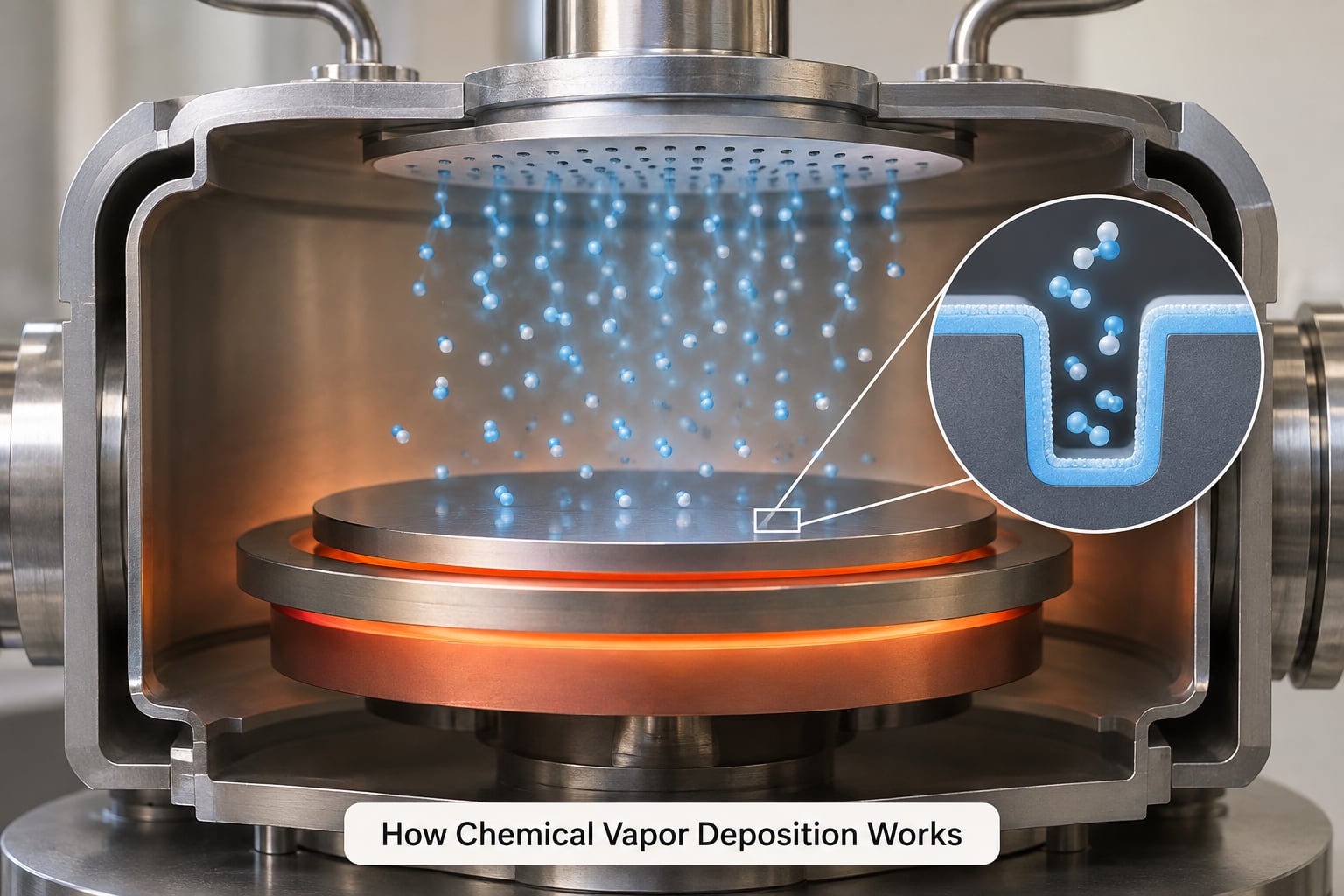
CVD depends on a chemical reaction. A volatile precursor enters a reaction chamber, decomposes or reacts on a heated surface, leaves a solid film, and carries volatile byproducts away in the gas stream.
Film growth is bottom-up. Precursor molecules adsorb onto the surface, react to leave a solid monolayer, and the byproducts desorb and are swept out, so the layer builds from the substrate upward rather than arriving as finished chunks of material.
Four variables steer the result, and engineers tune all of them together:
- Temperature sets the reaction rate and the film density. Hotter chambers usually give denser films with less hydrogen left in the lattice, which matters for dielectrics that have to survive later etching and ashing steps.
- Pressure controls how far the reaction happens in the gas phase versus on the surface. Low pressure pushes chemistry toward the surface and usually improves step coverage; atmospheric pressure is faster but more prone to particles.
- Chemistry determines composition. Titanium nitride from titanium tetrachloride, nitrogen and hydrogen at around 1000 degrees C is the classic hard-coating reaction, and silicon nitride and silicon oxide follow the same pattern with different precursors.
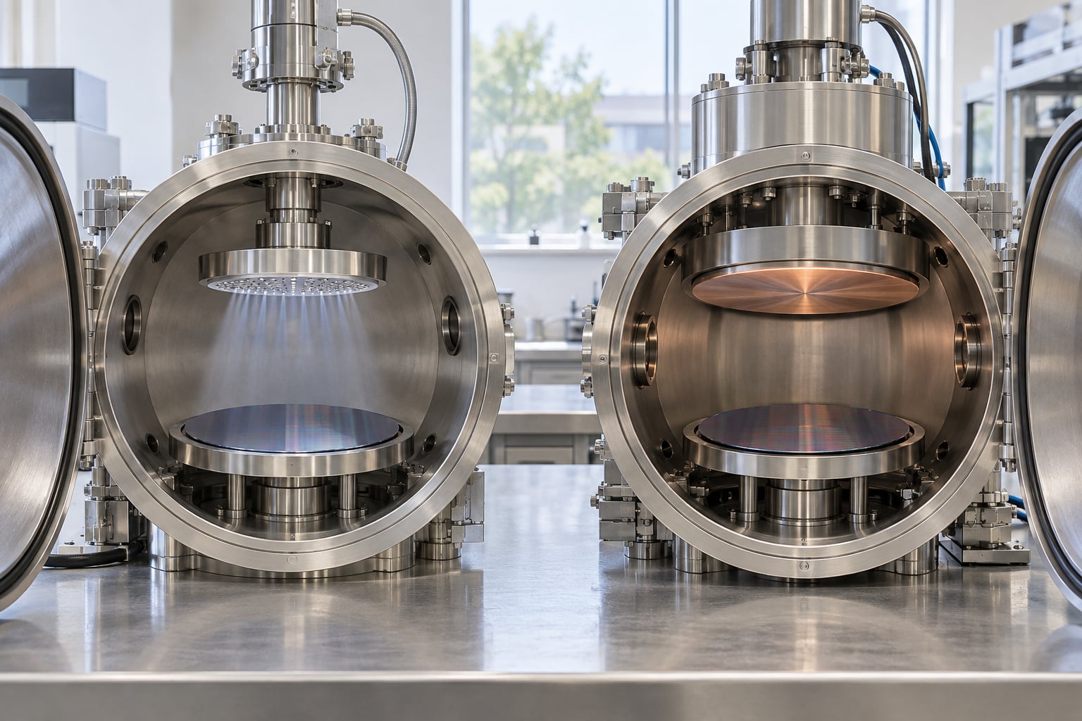
- Precursor delivery decides uniformity across a wafer. Meters control flow, and a showerhead distributes gas across the wafer so every die sees the same partial pressure.
The main variants differ mostly in how they supply energy. Low pressure CVD relies on substrate heat alone, plasma-enhanced CVD adds a plasma to break the precursor bonds at lower temperatures, atmospheric pressure CVD trades vacuum for throughput, metal organic CVD is built around organometallic sources, and atomic layer deposition is the extreme limiting case where each cycle deposits roughly one atomic layer.
How Physical Vapor Deposition Works
PVD transfers material physically. Nothing reacts. Atoms are knocked or boiled off a source, travel across the chamber, and condense on whatever is in their path.
The two workhorses are evaporation and sputtering. Thermal evaporation heats a crucible or boat until the material vaporizes, and electron beam evaporation focuses the heat so pure metals can be melted cleanly. Sputtering works the other way around: a plasma is struck in an inert gas, ions bombard the target, and momentum transfer knocks atoms free of it.
Several process knobs control what lands on the wafer. Magnetron sputtering adds magnetic fields that trap electrons near the target and raise the deposition rate. Substrate bias drives energetic ions into the growing film, which densifies it and improves adhesion. Reactive sputtering admits a small amount of reactive gas, so a metal target becomes a compound. Chamber pressure and gas flow set the mean free path, which determines how much directionality the incoming flux keeps.
Cathodic arc evaporation runs an arc between an anode and the target, melting spots on its surface and ejecting ions from them, which is fast and works well for hard and decorative coatings. Ion beam deposition takes a different approach entirely, sending a beam from a dedicated source onto the part, at the cost of throughput and chamber size.
That physical transfer is also the weakness. The flux is a beam, so PVD is a line-of-sight process. Where a surface faces away from the target, it gets less material or none at all.
Film Quality, Uniformity, and Step Coverage
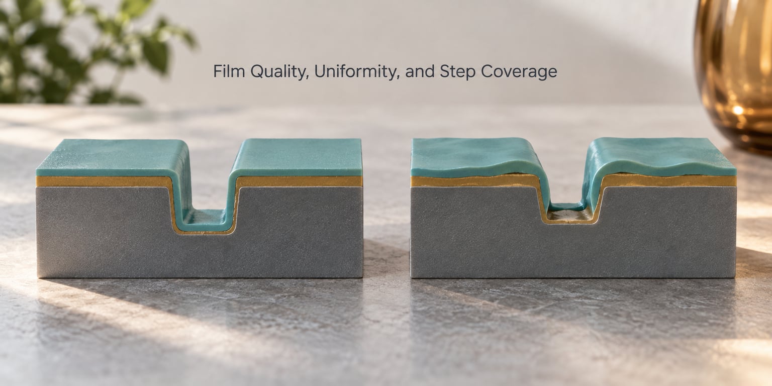
CVD wins on step coverage because the reacting gas reaches every exposed surface. Inside a trench with an aspect ratio of 5 to 1, a conformal CVD film lays down a similar thickness on the sidewall, the floor and the top surface, which is exactly what a contact or via needs.
PVD struggles in the same geometry. The sidewall is shadowed by the trench lip, so the bottom of a deep feature receives very little material, and the result is a pinched, discontinuous film. Long before modern high-aspect-ratio structures, this was already visible in shallow metal interconnect trenches, which is why CVD and ALD took over barrier and seed deposition while PVD was pushed out of the deep features.
Wafer-scale uniformity is closer than people expect. With good showerhead design, mass flow control and temperature control, CVD holds thickness within a few percent across a wafer. PVD reaches similar numbers for flat, facing surfaces because the target can be sized and shaped to the geometry, but uniformity degrades in proportion to how far the surface tilts away from the source.
Defect profiles also differ. CVD generates particles when a precursor condenses in the gas phase, so chamber condition and gas purity carry more weight. PVD runs cool and inert, which is simpler to control, but arc processes can throw droplets and sputter processes can flake the target if it runs at high power for too long.
Neither is automatically worse. Process design moves the ceiling: a sputtered film with high ion energy and a proper nucleation layer can close small pinholes, and a CVD recipe run at a lower pressure can be pushed to cover harsher topographies than its usual work.
Materials and Film Properties
PVD covers metals and alloys: aluminum, copper, titanium, tantalum, nickel, gold, chromium and their alloys all deposit cleanly by evaporation or sputtering. Metals with high melting points, including tungsten and molybdenum, are easy because sputtering does not need the source to melt. Nitrides and carbides are reachable in PVD through reactive sputtering or by sputtering from a compound target.
CVD covers the materials PVD handles awkwardly. Silicon dioxide, silicon nitride, silicon carbide, the family of deposition dielectrics used in logic and memory, are routine CVD and ALD work. It also deposits semiconductors epitaxially, which means growing a single crystal layer on a wafer rather than laying down a polycrystalline film, a capability PVD simply does not have.
Film properties follow from the mechanism. CVD films are denser and lower in hydrogen at higher temperature, which means lower leakage and a more predictable dielectric constant. PVD films are purer in the sense that the source metal is transferred without reaction, and they are easier to deposit as a single element rather than a compound.
Adhesion is the real difference. CVD coatings often form a chemical or diffusion bond with the substrate, so they resist galling and shear in metal forming. PVD gives a physical bond that is weaker in exactly those conditions, which is why a diffusion bond layer is often added underneath. Residual stress also behaves differently: PVD can deposit compressive or tensile films by adjusting ion energy, while CVD stress is governed mostly by the substrate temperature and the cooling rate.
Both deposit multilayers. PVD superlattices are a deliberate tool for hard coatings, alternating hard and soft layers to block dislocation motion. CVD builds multilayers by changing precursor flow, which is slower and less flexible but works in geometries PVD cannot reach.
Deposition Rate, Temperature, and Equipment Cost
CVD is the slower and hotter of the two. Deposition rates are quoted in nanometers per minute and depend heavily on the chemistry, but even fast processes run well below what a high-power sputter tool delivers. Thermal budget is the harder limit: CVD typically operates between 500 and 1100 degrees C, while PVD commonly sits between 200 and 500 degrees C.
That temperature gap decides a lot. Tool-grade CVD often runs near 1000 degrees C, which is why engineers worried about high speed steel end mills losing concentricity and hardness in the furnace. PVD at lower temperature leaves a precision-ground part dimensionally untouched, which is why it is the default for precision tooling.
Consumables differ too. CVD burns precursor gas, and in tool coatings the halogenated precursors are expensive, toxic, and generate acidic byproducts that need scrubbers and monitored gas cabinets. PVD consumes target material, which is cheaper to handle, plus inert process gas, and the exhaust is far less of a hazard. A small shop that can run a sputter system but has no scrubber or gas supply infrastructure is realistically limited to PVD.
Neither is uniformly cheaper. CVD charges more per run in time, energy and gas handling. PVD charges more in chamber complexity and in the fact that a failed run can consume part of a target and a lot of pump time. Comparing the two only by equipment purchase price is the most common mistake, because the real cost sits in throughput, rework and how many parts the process actually delivers per week.
Lead times in the trade follow the same split. Functional PVD coatings typically come back in two to five working days, and CVD runs longer, commonly five to seven.
Chemical Vapor Deposition vs Physical Vapor Deposition: Which Is Better?
Neither is better in general. CVD is better when the geometry is hard and the film has to be dense and conformal, and PVD is better when the part is precision work and the layer is a metal or a hard coating.
Choose CVD when the structure has deep trenches or vias, when the film is a dielectric with tight leakage requirements, when the layer is epitaxial, or when the coating must survive galling and shear. The chemical bond it forms with the substrate is the deciding factor for forming dies and draw dies, and no amount of adhesion layer makes a PVD film match it there.
Choose PVD when the substrate is heat sensitive or precision ground, when the film is a metal interconnect, seed or barrier layer, when the part needs masked or selective areas, or when throughput matters more than conformality. PVD also wins for decorative finishes, where a thin, colorful, well-adhered film on a watch case or a bathroom fitting is the entire goal.
The honest summary is that the two are complements, not competitors. Many production flows use both in the same build, with a PVD adhesion layer under a CVD dielectric, or a PVD metal fill followed by a CVD liner.
Which Should You Choose?
Start from the layer, not from the process. Here is how the choice usually lands in semiconductor and electronics work.
- Interconnect metals such as aluminum and copper wiring go to PVD, because the surfaces are planar and metal purity matters most.
- Barrier and seed layers in deep structures go to CVD or ALD, because step coverage decides whether the layer is continuous or pinched.
- Dielectric layers for interlayer insulation, passivation and hardmasks are CVD work, since the required density and pinhole control come from the chemistry.
- Capacitors split between the two: PVD or CVD for the electrode, CVD or ALD for the high-k dielectric, and PVD for the hard mask and structural layers.
- Optical and anti-reflective coatings are PVD. The layers are thin, the geometries are gentle, and index control matters more than step coverage.
- Advanced logic and memory structures lean CVD and ALD as the aspect ratios grow, and PVD survives mainly for the metal and nitride layers that sit on flat ground.
Two checks close most decisions. If masking matters, PVD wins, because selective deposition with CVD means leaving extra stock and grinding critical dimensions afterwards. If the part is high speed steel or anything else that changes properties with heat, PVD wins on temperature alone.
Atomic layer deposition is worth a look when the requirement sits between the two. It is a CVD variant run in self-limiting cycles, and it deposits a fraction of a nanometer per cycle with excellent conformality. It is the right answer for a barrier in a high-aspect-ratio contact and the wrong answer when you have thousands of wafers to run this week.
Frequently Asked Questions
What is the main difference between CVD and PVD?
PVD transfers material physically. Atoms are evaporated or knocked off a solid target by sputtering and travel in a line-of-sight beam to the part. CVD forms the film chemically, by reacting volatile precursor gases on or near a heated substrate, so the material arrives as a reaction product rather than as transferred atoms. That single difference explains most of the practical contrasts between the two.
Is CVD more conformal than PVD?
Yes, by a wide margin, and it is the main reason to choose CVD. The reacting gas in CVD reaches every exposed surface, so sidewalls, trench floors and via bottoms receive a similar thickness. PVD flux behaves like a beam, so surfaces facing away from the target are shadowed and deep features get little or no film. For anything with a high aspect ratio, conformality is where CVD wins outright.
Which method deposits metals and which deposits dielectrics?
Both can deposit metals. PVD is the traditional route for aluminum, copper, titanium, tantalum, nickel and gold, and it also forms compound films through reactive sputtering. CVD handles the dielectrics: silicon dioxide, silicon nitride, silicon carbide and high-k materials, where the chemistry is what delivers the density and composition the device needs. In practice, a fab uses PVD for metals on flat surfaces and CVD for the dielectrics and the liners.
Does CVD or PVD provide better step coverage in trenches?
CVD. The precursor gas distributes throughout the chamber and reacts wherever it lands, so a trench with a high aspect ratio still gets a continuous coating on the sidewalls and floor. PVD depends on straight-line travel from the target, so the trench lip shadows the bottom and the film pinches or breaks. This is why barrier and seed layers moved from PVD to CVD and then to ALD as trench and via aspect ratios climbed.
Can physical vapor deposition be used for high-aspect-ratio structures?
Only with help. Plain PVD covers the top surface and the upper sidewalls, then runs out of flux as the feature gets deeper. PVD can be pushed further by rotating the part, stepping the target past it, increasing working gas pressure to scatter the flux, and adding an ion source that steers bombardment at an angle. Those tricks extend coverage but never match CVD, and they add cycle time. For deep structures, change process.
How do I choose between CVD and PVD for a semiconductor process?
Decide the geometry first, because it is the hardest constraint. Deep or high-aspect-ratio features push you to CVD or ALD; flat surfaces leave the choice open. Then check the required film properties, whether it is a metal, a dielectric or an epitaxial layer, and how much thermal budget the wafer and the stack below can afford. Finally confirm the tooling can handle it, since CVD needs precursor supply, scrubbers and gas monitoring that a PVD line may not have.
Conclusion
There is no winner between CVD and PVD, only the right fit for the layer in front of you. Define the required film properties, the structure geometry, the material and the throughput you need, then match the process to the hardest of those four. Geometry decides more cases than anything else: deep features point to CVD or ALD, flat surfaces and heat-sensitive parts point to PVD.