Thermal oxidation is the process of growing a silicon dioxide (SiO2) layer directly on a silicon wafer by heating it in an oxygen or water-vapor ambient at roughly 800 to 1200 C. Unlike a deposited film, the oxide is formed by consuming silicon from the wafer itself, which leaves a dense film with an exceptionally clean Si/SiO2 interface.
That single difference, growth versus deposition, is the mental model that makes the rest of the process predictable. Once you know the film is being made out of the wafer, the questions that follow answer themselves: how thick it can get, how the thickness grows with time, and why the interface holds up better than anything you can deposit on top.
The one piece of history worth keeping in mind comes from Fairchild Semiconductor in 1965, when Bruce Deal and Andrew Grove published the kinetic model that still governs furnace design. It has been refined, patched and occasionally ignored for sixty years, and it is still the first thing a process engineer reaches for when someone asks how long a run takes.
Table of Contents
- What Is Thermal Oxidation in Wafer Processing?
- How Thermal Oxidation in Wafer Processing Works
- Where the reaction actually happens
- Why the film grows in both directions
- What the Deal-Grove model says
- What the substrate does to the rate
- What Are Dry Oxidation and Wet Oxidation?
- How Do Temperature and Time Control Oxide Thickness?
- A worked calculation at 1000 C
- Where the model stops being useful
- What Equipment Is Used for Thermal Oxidation?
- Why Is Oxide Thickness and Quality Important?
- How Does Thermal Oxidation Compare with Other Dielectric Processes?
- What Are the Main Thermal Oxidation Process Challenges?
- Thickness variation across the boat
- Bird’s beak at masked edges
- Photoresist lifting on steam oxide
- Particles and contamination
- Thermal budget
- How Do You Verify the Oxide Layer?
- Frequently Asked Questions
- What is thermal oxidation in wafer processing?
- What is the difference between dry and wet oxidation?
- What is the Deal-Grove model?
- How do I calculate thermal oxide thickness?
- Why does (111) silicon oxidize faster than (100)?
- Is thermal oxide better than PECVD oxide?
- Conclusion
What Is Thermal Oxidation in Wafer Processing?
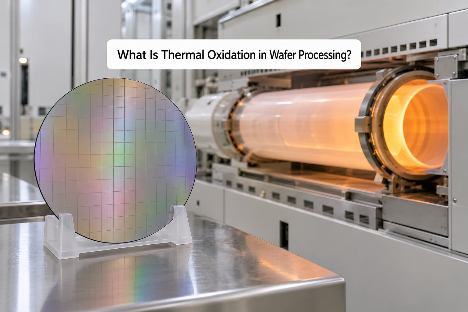
Thermal oxidation in wafer processing is a thermal process step, not a coating step. A bare or partially processed wafer sits in a high-temperature ambient containing oxygen, water vapor, or a mixture, and the silicon surface converts to SiO2 in place.
The word that matters is silicon wafer oxidation. The wafer loses material. When you grow a 500 nm thermal oxide, roughly 230 nm of the silicon surface is consumed to make it, which is why a heavily oxidized wafer is measurably thinner and slightly more warped than the one you started with.
Where it sits in the front-end flow depends on what you are building. Thermal oxide goes down early, on bare or lightly doped silicon, before the first polysilicon deposition and usually before the source/drain implant. Later passes grow field isolation, gate oxide, or thin sacrificial layers after patterning steps, each one paying a thermal budget that later steps have to survive.
Silicon dioxide earns this position because of what it does rather than how exotic it is. It is an electrical insulator, it is stable on silicon at high temperature, it resists most wet etches, and its interface with the underlying silicon is close to chemically ideal. No deposited dielectric has matched that last point consistently, which is the entire reason the growth-versus-deposition distinction matters.
How Thermal Oxidation in Wafer Processing Works
Where the reaction actually happens
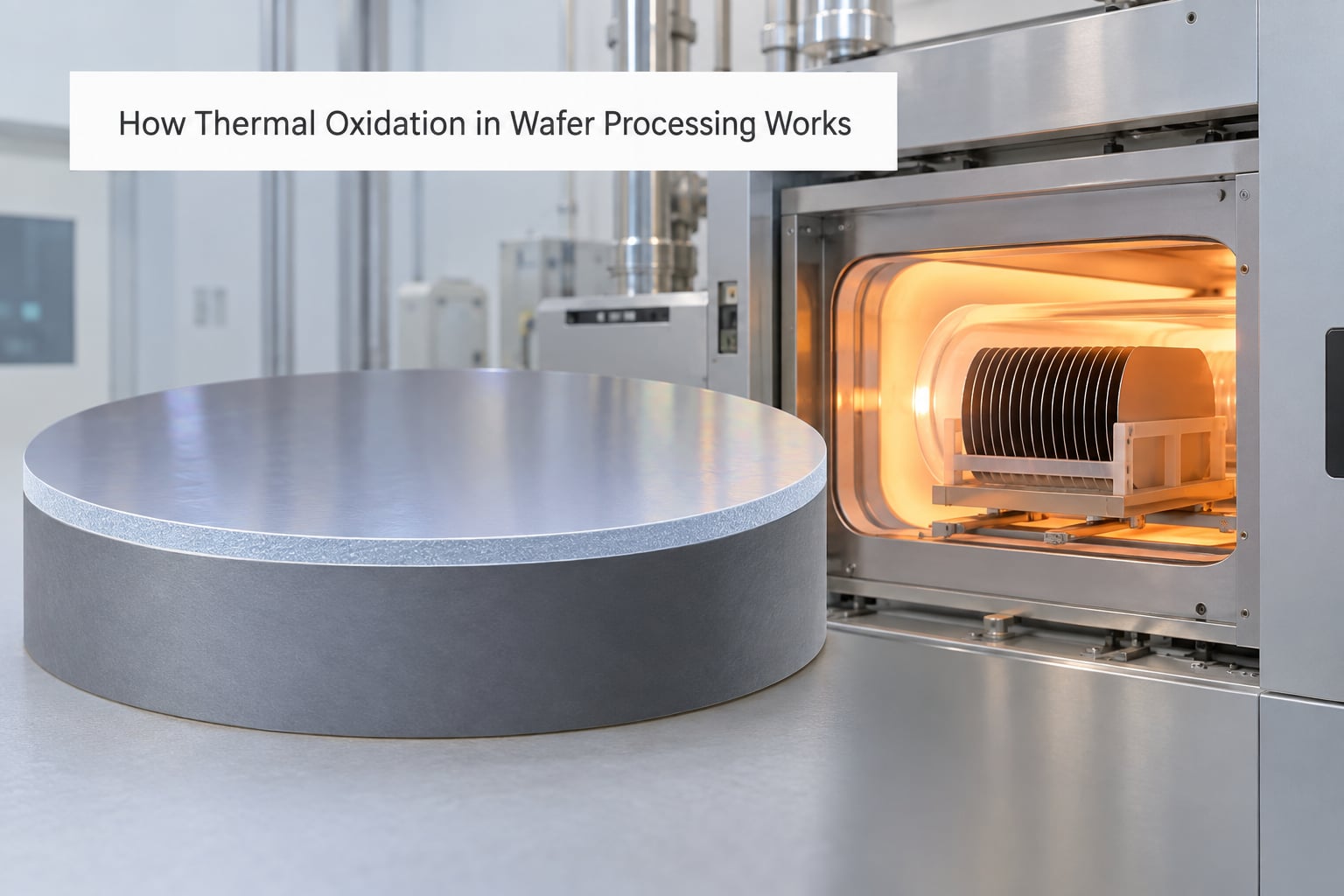
The reaction does not take place at the outer surface of the film. It takes place at the silicon-oxide boundary, and that single fact explains the whole growth curve. Oxygen or water vapor has to diffuse through whatever oxide already exists before it can reach fresh silicon and react with it.
Dry oxidation is the simple case: Si plus O2 becomes SiO2. Wet oxidation uses H2O vapor, which is far more soluble in the oxide film, so it diffuses through existing oxide much faster.
Why the film grows in both directions
When silicon converts to silicon dioxide, the new oxide occupies roughly 2.17 times the volume of the silicon that produced it. The film has to go somewhere, so it grows inward into the wafer and outward above the original surface, ending up with about 46 percent of its thickness below where the silicon started and 54 percent above.
This is not a curiosity. It is why oxidation has a thermal budget even when the target film is thin, because the reaction consumes part of the substrate.
What the Deal-Grove model says
Deal and Grove found that the process follows a simple relationship between film thickness x, process time t, and two empirically derived rate constants:
x squared + A x = B (t + tau)
A is the linear rate constant, B is the parabolic rate constant, and tau is a time shift that accounts for oxide already present before the run started. When you are growing on a bare, cleaned wafer, set tau to zero. When the wafer already carries film, tau is how you stop the model from pretending the new growth happened on bare silicon.
The two constants correspond to the two physical limits of the process. Early on, the surface reaction is slower than diffusion, so thickness grows linearly with time and the A term dominates. Later, the oxidant has to travel further through its own product, diffusion becomes the bottleneck, and growth slows down in proportion to x squared, which is what the B term describes.
That transition is not academic. A thin gate oxide is controlled almost entirely by temperature and surface chemistry, while a thick field oxide is almost entirely diffusion-limited, which is why pushing past a micrometer requires far more time than doubling the target thickness would suggest.
What the substrate does to the rate
Two substrate properties change the numbers. The first is crystal orientation: (111) silicon oxidizes roughly 1.7 times faster than (100) silicon, because the denser atomic packing presents a different surface geometry to the arriving oxidant. CMOS has used (100) wafers for exactly this reason, since slower growth is easier to control at the thicknesses that matter for a gate.
The second is doping. Heavily doped silicon oxidizes faster than lightly doped silicon, and the dopant itself redistributes at the interface as it grows. Boron tends to deplete at the interface while phosphorus and arsenic tend to accumulate, and both effects shift the electrical behavior of the finished device, not just the thickness.
What Are Dry Oxidation and Wet Oxidation?
Dry oxidation uses pure O2, wet oxygen uses a humidified O2 stream, and steam oxidation uses water vapor carried in a separate diluent. Most sources collapse the last two together, which is a mistake, because they behave differently in the furnace and produce different film chemistry.
| Property | Dry (O2) | Wet oxygen (humid O2) | Steam (H2O vapor) |
|---|---|---|---|
| Oxidant | Dry oxygen | Oxygen at controlled humidity | Water vapor in a diluent gas |
| Growth rate | Slowest | Fast | Fastest |
| Typical thickness role | Thin gate and thin masking films | Mid-range films | Thick field and isolation films |
| Film density | Highest | Intermediate | Lowest, most silanol content |
| Photoresist adhesion | Good | Variable | Poor without a surface treatment |
| Control difficulty | Most controllable | Depends on humidity delivery | Most sensitive to water quality |
Growth rate is the obvious divider, but film quality is the reason engineers pick one over the other. Dry oxide is dense, chemically stable and well behaved under a resist. Steam oxide grows fast, which is what you want for a two-micron field oxide, but it carries silanol (Si-OH) groups through the film. Those groups make the surface polar, and a non-polar photoresist sitting on top simply will not stick reliably, which is a recurring cause of lifted and torn patterning.
A third variant deserves mention because it is used where interface quality is the priority: chlorine-doped oxidation, where HCl or trichloroacetic acid is added to a dry run. The chlorine scavenges sodium and other mobile contaminants, traps charge at the interface, and consistently produces some of the lowest interface state densities available from a furnace.
How Do Temperature and Time Control Oxide Thickness?
Temperature is the strongest lever you have, and it is exponentially strong. Both rate constants follow Arrhenius behavior, so a change of 100 C can multiply the growth rate several times over, and the effect is steeper for wet oxidation than for dry. Time enters the same equation, but nonlinearly once you are past the linear regime.
| Process condition | What changes | What it means in practice |
|---|---|---|
| Lower temperature, longer time | Rate falls sharply, diffusion matters less | Thin films stay well inside the linear regime and hold thickness well |
| Higher temperature, shorter time | Rate rises sharply, more of the run is spent ramping | Usable for mid-range films, but ramp time is no longer negligible |
| Higher temperature, longer time | Parabolic term dominates early | Fast to a few hundred nm, then slows, and thermal budget grows quickly |
| Dry ambient | Lower solubility of oxidant in the film | Slower growth, denser film, tighter thickness control |
| Wet or steam ambient | Higher solubility of oxidant in the film | Faster growth, especially past about 100 nm |
A worked calculation at 1000 C
Worked example: a 100-minute dry run at 1000 C. Reference rate constants for that condition are commonly given as A equals 0.11 micrometers per hour and B equals 0.0117 square micrometers per hour. Rate constants vary between references and between tools, so treat these as working values and use your own fab data when the answer has to be exact.
Convert the run to hours first, because the constants are hourly. 100 minutes is 1.67 hours, and the parabolic term becomes B times t, which is 0.0117 times 1.67, or 0.0195 square micrometers. The equation is now x squared plus 0.11 x minus 0.0195 equals zero. Solving the quadratic gives x equal to negative 0.055 plus the square root of 0.003 plus 0.0195, which is negative 0.055 plus 0.150, so roughly 0.095 micrometers, or 95 nanometers.
Now check which regime you landed in, because that tells you whether the answer is trustworthy. The crossover thickness is B divided by A, which here is 0.106 micrometers. At 95 nanometers you are sitting almost exactly on it, so both terms contribute and neither approximation alone is safe. Differentiating the equation gives the instantaneous rate as B over (2x plus A), which here is 0.0117 over 0.30, or about 0.039 micrometers per hour, comfortably under the 0.057 average rate for the whole run. That gap is the parabolic slowdown showing up in a single number.
Reverse the problem and the shape of the curve becomes obvious. Reaching 0.5 micrometers takes x squared plus A x divided by B, which is 0.25 plus 0.055 over 0.0117, about 26 hours. Reaching 1.0 micrometer takes 1.0 plus 0.11 over 0.0117, about 95 hours. The second half micron costs roughly 69 hours against 26 for the first, so doubling the target thickness nearly quadrupled the run. That is the parabolic term doing its job, and it is the practical reason thick field oxides are grown wet rather than dry.
That same example answers the incremental question: a wafer already carrying 0.5 micrometers and needing 0.5 more does not get 26 hours. It gets about 95 minus 26, so roughly 69, because the second half micron grows against an existing barrier. Setting tau to a value that represents the prior run lets you solve for the total in one step instead of subtracting, which is how most fabs and most textbook problems handle it.
Where the model stops being useful
The Deal-Grove model is an empirical fit for conventional furnace oxidation in the range where it was measured. It degrades badly below roughly 25 nanometers, where surface chemistry, hydrogen chloride additions and pre-grow clean steps dominate the result, and it does not describe rapid thermal oxidation well because the ramp itself is a significant part of the process time.
What Equipment Is Used for Thermal Oxidation?
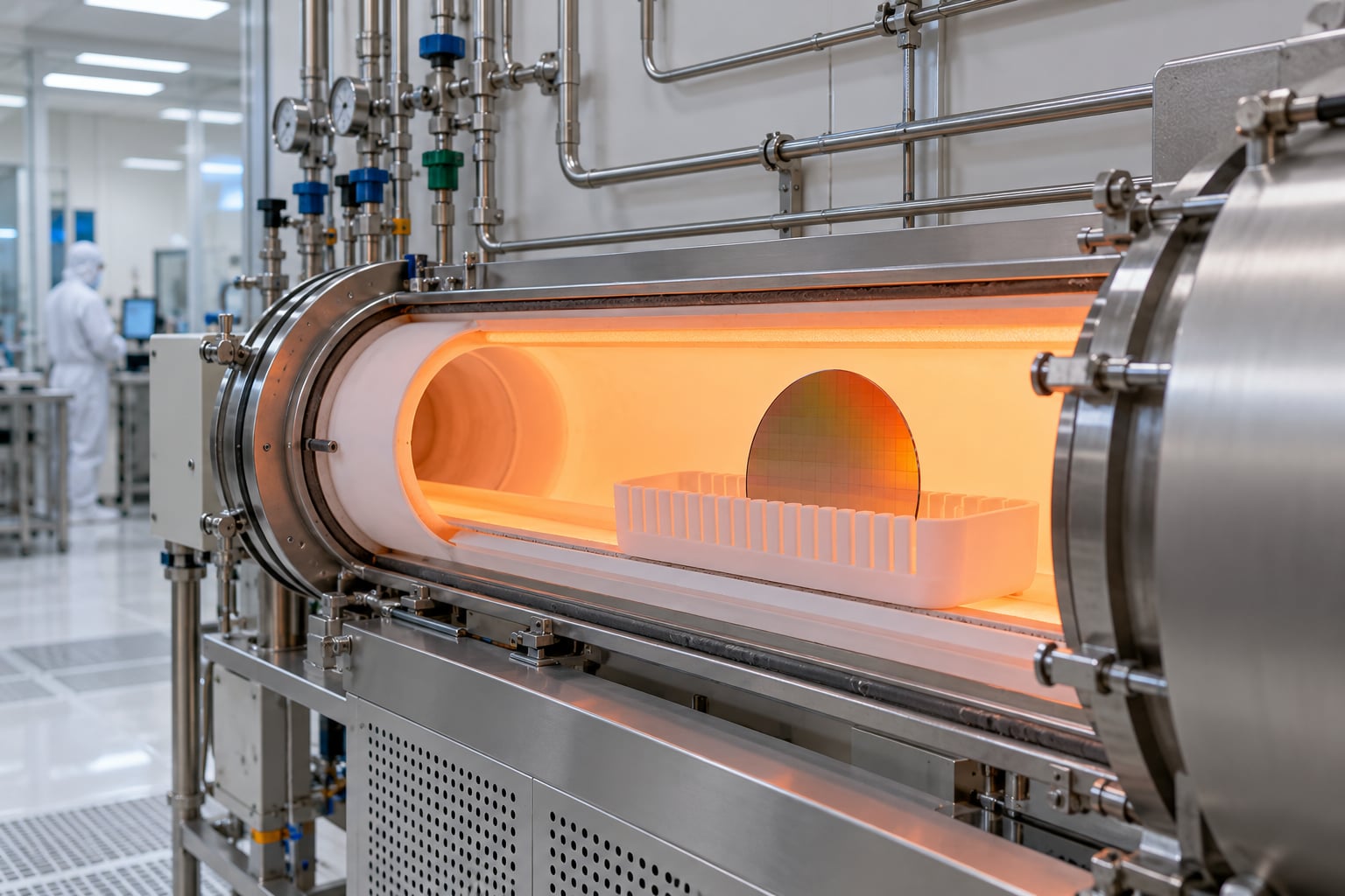
The workhorse is a resistance-heated batch diffusion furnace. The wafer sits on a quartz boat inside a quartz process tube, the tube is heated by resistive elements wrapped around it, and a controlled gas stream flows through it. Everything about the design is aimed at one goal, which is holding the whole boat at the same temperature with the same gas composition for the whole run.
Geometry comes in two flavors. A horizontal furnace lays the tube flat and pushes the boat in from one end. A vertical furnace stands the tube upright and lifts the boat in from above, which keeps the boat axis aligned with the gas flow and reduces how much the rising gas disturbs the wafers as they heat.
Quartz is the standard tube and boat material because it holds up to about 1100 C in oxygen without reacting with it. Higher temperature processes move to silicon carbide or other ceramic components, which introduces their own contamination concerns.
Gas delivery is where dry and wet runs diverge. Dry oxygen arrives through a straightforward flow controller. Wet oxygen is produced by bubbling oxygen through a water column or by a humidifier, so the humidity depends on water temperature and line conditions. Steam oxidation needs a separate water source, and the residual water content of the diluent gas has to be controlled tightly or the growth rate drifts.
Rapid thermal oxidation, usually called RTO or RTP, takes the opposite approach. A lamp array or a susceptor heater brings a single wafer to temperature in seconds, holds it briefly, and drops it again. Ramp rates on the order of tens to hundreds of degrees per second are possible, against a fraction of a degree per second in a batch furnace, and that is the entire point: the thermal budget collapses.
The hard problem in RTO is knowing the wafer temperature. A wafer reaches 1000 C in a few seconds and its emissivity changes as the surface goes from bare silicon to growing oxide to whatever is on top of it, so an infrared pyrometer reading drifts through the run. Wafers carrying a backside thermocouple avoid this, at the cost of the backside being unavailable for other work. RTO also processes one wafer at a time, so the economics only work for thin films, generally under about 40 nanometers.
Why Is Oxide Thickness and Quality Important?
Because oxide thickness sets capacitance, and capacitance sets how hard a transistor has to work. A gate dielectric thickness that runs thick raises the threshold voltage, cuts drive current, and pushes leakage up. A film that runs thin risks tunneling through the barrier. There is a narrow window, and thermal oxidation is the process that used to land in it reliably.
Thickness is not the whole quality story. Two films measuring the same 20 nanometers can behave very differently. The one with a clean interface has a low interface trap density and a predictable flatband voltage. The one grown on a contaminated surface has trapped charge that drifts, shifts threshold voltage under bias, and shows up as hysteresis in a capacitance-voltage measurement.
Where oxide is used, in rough order of how much the process depends on it:
- Gate dielectric. The highest-stakes use. Interface quality and thickness control both matter, and both drive device speed.
- Field isolation and LOCOS. Locally oxidized silicon, where a nitride mask defines regions and the oxide grows thick where it is exposed. Used to insulate adjacent devices.
- Etch and implant masking. A thin film that protects areas that must not be exposed. Consumed by the etch it protects against.
- Surface passivation. A film that reduces surface states and contamination on areas with no active device.
- Dopant barrier. A film that stops an implant from reaching somewhere it should not go.
- Sacrificial oxide in MEMS. A thick layer, up to roughly 20 microns in practice, that is later etched away to release a moving structure.
Masking use has a consequence people forget: the oxide that protects a region is consumed by the etch step it served, so the film has to be thick enough to survive that etch and still deliver the thickness the device needs.
How Does Thermal Oxidation Compare with Other Dielectric Processes?
Thermal oxide wins on interface quality and loses on temperature, throughput and conformality. Everything else follows from those two facts.
| Criterion | Thermal oxide | PECVD oxide | TEOS oxide | High-k ALD |
|---|---|---|---|---|
| Mechanism | Growth, consumes silicon | Deposition from plasma | Deposition from vapor | Deposition, self-limiting |
| Substrate temperature | High, 800 to 1200 C | Low, often 200 to 400 C | Moderate, 600 to 800 C | Low, 200 to 350 C |
| Si/SiO2 interface quality | Best available | Good with a pre-treatment | Good, denser than PECVD | Needs a capping layer |
| Conformality in trenches | Poor, grows from silicon only | Good | Good | Excellent |
| Contamination risk | Metal from furnace parts | Hydrogen from silane and ammonia | Carbon and fluorine residues | Alkali and rare-earth residues |
| Best use | Thin gate films, field oxide, masking | Passivation, liners, low thermal budget | Interlayer dielectric, dense films | Modern gate stacks below about 1 nm equivalent |
One more thing about growth mechanics catches people out. Thermal oxide grows from the silicon, so a trench coated with a deposited dielectric will not fill with oxide. Deposated methods coat conformally; thermal oxidation simply cannot. That is a hard physical limit, not a process tuning issue, and it is why the industry moved away from furnace gate oxide at small nodes rather than simply trying harder to grow thinner.
The modern node answer is a high-k dielectric deposited by ALD with a thin thermal or ALD’d silicon dioxide layer underneath as the interface. The growth-versus-deposition framing still holds, it just moved one layer down.
What Are the Main Thermal Oxidation Process Challenges?
Thickness variation across the boat
This is the most common and least dramatic problem. Wafers closer to the gas inlet or sitting at the ends of the boat see a slightly different gas composition and temperature than those in the middle, and they come out with a different thickness. Loading pattern, boat position, and gas flow rate all shift it. The fix is a characterization map, not a recipe change: measure a grid of points per run and spread the process window with the distribution you find.
Bird’s beak at masked edges
Where a masking layer ends, the growing oxide does not stop with a vertical wall. It creeps under the mask edge, consuming silicon laterally and producing a curved feature that eats into the area you wanted to keep. The bird’s beak gets worse as the oxide gets thicker and the mask gets thinner, which is why the industry moved to shallow trench isolation rather than pushing LOCOS further. If you inherit a LOCOS process, expect a minimum field oxide thickness and a minimum nitride thickness tied to it.
Photoresist lifting on steam oxide
Silanol groups make steam-grown oxide polar, and the resist on top of it is not. The result is edge lifting and tearing during develop, usually in the middle of a dense pattern. A dehydration bake before coating, a short silane-based adhesion treatment, or falling back to dry oxidation for films thin enough to tolerate the slower growth are the usual responses.
Particles and contamination
The quartz tube and boat are a large surface area sitting at high temperature in an oxygen flow. A flake from a previous process, a defect in a boat paddle, or a scratched quartz part will redistribute wafers in a run without warning. Preventive maintenance schedules on the tube and boat matter more than most process changes, and metal from the resistance elements is the reason some fabs use silicon carbide tubes at the highest temperatures.
Thermal budget
Every oxidation run pushes the wafer through temperatures that activate dopants, move junctions, and anneal out damage the implant created. A step that looks like a 90-minute push can undo a careful implant profile. This is why modern flows are aggressive about raising temperature and shortening time, and why the reason a given step is a furnace rather than an RTO is almost always thermal budget rather than throughput.
How Do You Verify the Oxide Layer?
Thickness measurement is routine. The harder question is whether the film is good, and that needs more than a number.
Ellipsometry is the standard thickness tool. It measures the change in reflected light polarization caused by the film’s refractive index and thickness, and it works on the same principle for thermal oxide, PECVD oxide and photoresist. It is fast and non-destructive, which is why it is the first thing anyone reaches for. Reflectometry works the same way and is used where the metrology is already in place.
FTIR looks at absorption bands in the infrared. It will pick up the silanol signature that signals a wet-grown film, and it can compare an interface against a reference to detect non-stoichiometric silicon-rich oxide near the boundary. Slower than ellipsometry, and used when film chemistry matters more than the thickness number.
Profilometry measures a step in the film directly, typically by scratching or etching a deliberate opening in the film and measuring the height difference. It is slow and destructive, and it exists mainly to calibrate the faster optical tools.
For anything that will carry a gate, add electrical verification. A capacitance-voltage measurement across the oxide reports the flatband voltage and any hysteresis from trapped charge, and a time-dependent dielectric breakdown measurement reports reliability. A film that passes ellipsometry and fails breakdown is a real and common outcome, and it usually points at a defect or a particle rather than a thickness problem.
Sampling strategy matters as much as the tool. One point in the center of a 300 mm wafer tells you very little. Map points across the radius and include wafers at both ends of the boat, then track the map over several runs to see whether variation is random or structured.
Frequently Asked Questions
What is thermal oxidation in wafer processing?
Thermal oxidation is growing a silicon dioxide film directly on a silicon wafer by heating it in an oxygen or water-vapor ambient at roughly 800 to 1200 C. Because the oxide is formed by consuming silicon from the wafer itself rather than being deposited on top, the resulting film is dense and its interface with the underlying silicon is exceptionally clean. That interface quality is why thermal oxide remained the benchmark dielectric for decades.
What is the difference between dry and wet oxidation?
Dry oxidation uses pure O2, and wet oxidation uses water vapor or humidified oxygen. Water vapor is far more soluble in the oxide film, so it diffuses through existing oxide faster and grows the film more quickly, which is what makes wet oxidation the choice for thick field oxides. Dry oxidation grows more slowly but produces a denser, more stable film that holds up better under a photoresist, so it stays the standard for thin gate and masking layers.
What is the Deal-Grove model?
The Deal-Grove model is the empirical kinetic relationship between thermal oxide thickness and process time, written as x squared plus A x equals B times t plus tau. A is the linear rate constant and controls early growth, when the surface reaction is the bottleneck. B is the parabolic rate constant and controls later growth, when diffusion through the film takes over. Tau is a time shift for oxide already present before the run. Deal and Grove published it in 1965 at Fairchild Semiconductor.
How do I calculate thermal oxide thickness?
Use the Deal-Grove equation x squared plus A x equals B times t plus tau, with rate constants taken for your ambient, temperature and crystal orientation. Set tau to zero for a bare cleaned wafer. To find thickness from a known time, substitute t and solve the quadratic for x. To find time for a target thickness, plug in x and solve for t. Below about 25 nanometers the model loses accuracy, so measure rather than calculate at that scale.
Why does (111) silicon oxidize faster than (100)?
The two surfaces present different atomic arrangements to arriving oxygen, and the (111) plane oxidizes roughly 1.7 times faster than the (100) plane. The difference comes from how many silicon bonds per unit area face the oxidant, which changes the local reaction rate at the interface. CMOS has used (100) wafers partly for this reason: slower growth is easier to control at gate thicknesses, and the interface quality is more favorable.
Is thermal oxide better than PECVD oxide?
For a gate dielectric, thermal oxide is usually better, because its interface with silicon has lower trap density than anything deposited. For passivation layers, liners and interlevel dielectrics, PECVD often wins, because it deposits at a few hundred degrees and conforms to topography. PECVD also contains more hydrogen, which is a reliability concern for anything carrying a field. The real limit of thermal oxide is that it grows only from silicon, so it cannot fill a trench.
Conclusion
Start where the constraint actually is. Fix the required oxide thickness and the interface quality the device needs, then check what thermal budget is left for the step and what equipment you actually have. Those four answers, not a rule of thumb, choose the ambient and the temperature. Everything after that, from the rate constants to the run time, is arithmetic once the constraints are set.